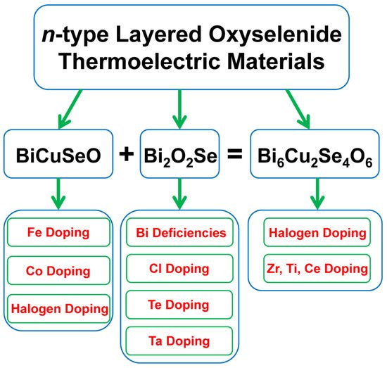
Bi6Cu2Se4O6is a new type of layered oxyselenide thermoelectric material. The crystal structure of Bi6Cu2Se4O6can be regarded as a 1:2 ratio of BiCuSeO and Bi2O2Se heaping along thec-axis by turns, so there are insulative layersBi2O22+and conductive layersCu2Se22−andSe2−in the structure. The Bi6Cu2Se4O6system not only maintains the low thermal conductivity of BiCuSeO but also can utilize the intrinsic electron carrier concentration of Bi2O2Se, considered to be a promisingn-type oxyselenide thermoelectric material.
- thermoelectric
- -type oxyselenide
- BiCuSeO
- BiOSe
1. Introduction
Thermoelectric (TE) materials can achieve the direct transition between heat and electricity without producing other pollutants, providing an effective solution to the energy crisis and environmental problems [1][2][1,2]. The dimensionless figure of merit ZT defines the efficiency of a thermoelectric device, which derives from three related physical quantities: electrical conductivity ( σ ), Seebeck coefficient ( S ) and thermal conductivity ( κ ), Z T = ( σ S 2T / κ ) , with absolute temperature T . However, the tightly-coupled relationship among these parameters makes it difficult to improve the overall ZT [2][3][4][5][6][2,3,4,5,6].
Intrinsic p -type semiconductor BiCuSeO possesses a layered ZrCuSiAs structure with space group P4/nmm [2][7][2,32]. The special layered crystal structure of BiCuSeO is constituted by insulative [ Bi 2O 2] 2+ layers and conductive [ Cu 2Se 2] 2− layers heaping along the c -axis by turns [8][9][33,34]. Due to the weak Van der Waals interaction between layers [10][11][12][13][9,35,36,37], the large displacement of the Cu atom [14][15][38,39] and the heavy Bi atom [3][16][17][3,40,41], BiCuSeO has intrinsically low thermal conductivity [18][42], which is an inherent advantage as a thermoelectric material. However, most of the reported BiCuSeO are p -type semiconductor materials at present, and researches on n -type BiCuSeO are relatively few and unsuccessful. The main problems are that no effective electronic dopant was found, and BiCuSeO-based materials with stable n -type transport properties have not been obtained yet.
Different from BiCuSeO, the intrinsic Bi 2O 2Se exhibits n -type transport properties due to a large number of Se vacancies in the crystal structure [19][20][43,44]. However, the crystal structure of Bi 2O 2Se is very similar to BiCuSeO in which insulative [Bi 2O 2] 2+ layers and conductive [Se] 2− layers stack along the c -axis alternatively [21][22][23][26,45,46]. Similarly, Bi 2O 2Se also has intrinsically low thermal conductivity due to the weak interlayer interaction [21][24][25][26][26,47,48,49], but its intrinsic carrier concentration (~1.5 × 10 15 cm −3 ) is too low, resulting in poor electrical transport performance [27][28][50,51]. Therefore, current research is mainly focused on increasing the carrier concentration, thus improving the electrical transport performance of Bi 2O 2Se.
Recently, several studies on n -type layered oxyselenide thermoelectric materials were reported, which motivates us to systematically summarize the recent progress of these researches. The outline of this review is shown in Figure 1 . First, several attempts to realize n -type BiCuSeO are summarized. Then, some typical approaches to optimize the thermoelectric performance of Bi 2O 2Se are presented. Next, a new type layered oxyselenide Bi 6Cu 2Se 4O 6 is introduced, and n -type transport properties can be obtained through halogen doping and optimized by introducing transition metal elements. At last, some prospective and outlooks were provided for future research in the end.
2. Various Attempts to Realize n-Type BiCuSeO
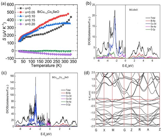
The peak Seebeck coefficient and corresponding temperature increase with the increase in Fe content, indicating the increase of band gap in those samples. Clearly, n -type transport properties can be found in the x = 0.03 sample at a low-temperature range, indicating that appropriate Fe content can achieve n -type BiCuSeO in a circumscribed temperature range.
Figure 2 3 a shows the temperature-dependent Seebeck coefficient ( S ) for Co-doped samples. For x = 0.05 and 0.10 samples, the S is positive within the entire temperature boundaries, indicating the dominant carrier is p -type. However, when the doping content of Co reaches 15%, the S begins to appear negative, indicating that the system exhibits n -type electrical transport properties. The negative S values of x = 0.20 sample within the entire temperature region indicate stable n -type electrical transport properties in the BiCuSeO system below room temperature.
Zhang et al. designed a series of continuous experimental steps to obtain n -type BiCuSeO [30][61]. Firstly, considering that the existence of Bi/Cu vacancies is the main reason for the p -type behavior of pristine BiCuSeO [31][32][62,63], extra Bi/Cu was introduced into the matrix to fill the vacancies which may produce holes. Finally, the optimal concentrations of extra Bi and Cu are determined as x = 0.04 and 0.05, respectively. To increase electron carrier concentration, halogen elements (Br, I) were selected as donor dopants at Se sites and introduced into the Bi 1.04 Cu 1.05 SeO matrix. The S as a function of temperature for I/Br doped Bi 1.04 Cu 1.05 SeO samples is presented in Figure 34 a,b. The introduction of Br/I can successfully transform Bi 1.04 Cu 1.05 SeO from p -type to n -type within a certain temperature range, and the negative S for I-doped Bi 1.04 Cu 1.05 SeO traverses a narrower temperature range than Br-doped one. In the high-temperature range, p -type behavior appears again, indicating that vacancies reproduced as the temperature rises, which may be relevant to the instability of Cu–Br and Cu –I bonds [33][34][64,65].
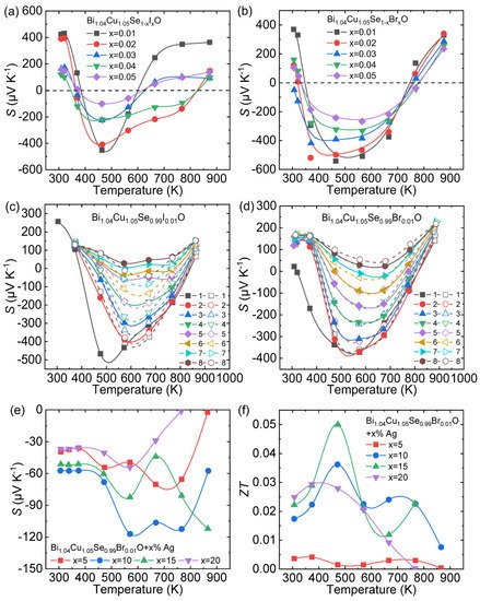
In order to further explore the p - n - p -type behavior in the obtained system, a heating–cooling measurement was carried out for halogen doing BiCuSeO samples [35][66], as shown in Figure 34 c,d. As can be seen, Bi 1.04 Cu 1.05 Se 0.99 X 0.01 O (X = Br, I) changes completely from n -type to p -type transport behavior after eight heating–cooling cycle measurements. The above results indicate that halogens are effective dopants to obtain n -type BiCuSeO but exhibit poor stability. To improve the stability of n -type transport, metallic particles were introduced into the halogen-doped Bi 1.04 Cu 1.05 SeO. The temperature dependence of S for Bi 1.04 Cu 1.05 Se 0.99 Br 0.01 O + x % Ag samples is negative within the entire temperature range, and the maximum | S | is ~125 μV/K ( Figure 34 e). The maximum ZT ~0.05 can be reached at 475 K in Bi 1.04 Cu 1.05 Se 0.99 Br 0.01 O + 15% Ag ( Figure 34 f).
3. Various Attempts to Enhance Thermoelectric Properties of Bi2O2Se
At room temperature, the σ hikes from ~0.019 S cm −1 for Bi 2O 2Se to ~101.6 S cm −1 for Bi 2O 2Se 0.985 Cl 0.015 , and then declines obviously as the Cl content increases ( Figure 47 a). One Cl − doped into the Se 2− sites can provide an extra electron, and the measured carrier concentration increased from 1.5 × 10 15 cm −3 to 1.38 × 10 20 cm −3 ( x = 0.015). However, when the Cl content exceeds the solubility limit, the formation of the low-conductivity second phase Bi 12O 15Cl 6 [36][69] will reduce the effective doping amount of Cl, thereby deteriorating the σ . The small polaron hopping conduction theory was chosen to study the impact of Cl dopant on the σ . This theory could be expressed as the following Formula (5) [37][70]: (5) σ = n e μ = ( C T ) exp ( − E a k B T ) where n , e , μ , C , k B , E a and T express the carrier concentration, carrier charge, carrier mobility, the pre-exponential terms, Boltzmann constant, activation energy and the absolute temperature, respectively. Figure 4 7 b shows the linear relationship between ln( σT ) and 1000/ T , and the E a can be obtained by calculating the slope of the straight line. As shown in the inset of Figure 47 b, the E a of Cl-doped samples is obviously lower than Bi 2O 2Se, indicating that the introduction of Cl is conducive to carrier excitation. In summary, the high σ achieved in Cl-doped Bi 2O 2Se is estimated to be the result of higher n coupled with lower E a .
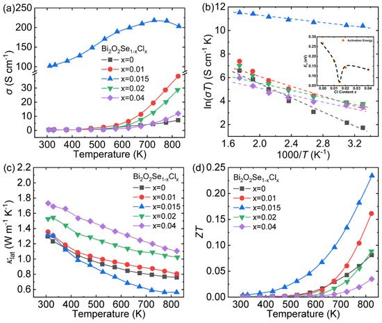
Lattice thermal conductivity ( κ lat ) of Bi 2O 2Se 0.985 Cl 0.015 declines evidently after 423 K, reaching the lowest value ~0.56 W m −1 K −1 at 823 K ( Figure 47 c). This effective decrease in κ lat is derived from point defect scattering introduced by Cl substitution coupled with the enhanced grain boundaries scattering. However, for the Bi 2O 2Se 0.98 Cl 0.02 and Bi 2O 2Se 0.96 Cl 0.04 sample, the considerable augment in κ lat is the result of the secondary phase Bi 12O 15Cl 6.
Benefitting from both the enhancement of the σ and the depression of the κ tot , the peak ZT value ~0.23 at 823 K is achieved in Bi 2O 2Se 0.985 Cl 0.015 ( Figure 47 d), which demonstrates that Cl is an effective dopant to optimize the thermoelectric performance of Bi 2O 2Se.
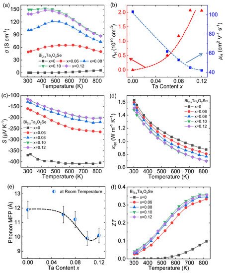
The carrier engineering and hierarchical microstructure by Ta doping remarkably enhance the ZT values in Bi 1.90 Ta 0.10 O 2Se, reaching ~0.30 at 773 K, which is an increase of ~350% compared to pristine Bi 2O 2Se ( Figure 59 f).
4. Attempts to Realize a New Kind of n-Type Oxyselenide: Bi6Cu2Se4O6
Because of the strong phonon scattering caused by layered structure [10][9], the lone pair electrons of Bi 3+ [39][40][78,79], and the local vibration of Cu + [14][38], BiCuSeO exhibits inherent low thermal conductivity. Another well-known thermoelectric oxyselenide, Bi 2O 2Se reveals stable n -type transport properties due to Se vacancies [19][20][43,44]. To fully utilize the features of BiCuSeO and Bi 2O 2Se, a new type layered oxyselenide Bi 6Cu 2Se 4O 6 was synthesized through solid state reaction (SSR) with the 1:2 ratio of BiCuSeO and Bi 2O 2Se ( Figure 610 a) [41][42][43][28,29,30], and stable n -type conductive transports were observed in this system through halogen element doping [42][29].
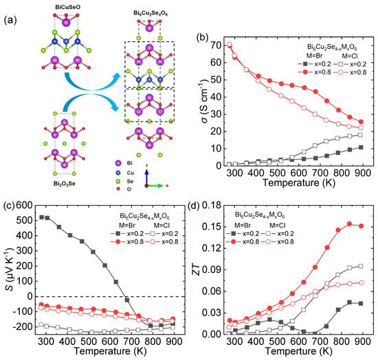
The σ of Cl-doped Bi 6Cu 2Se 4O 6 is higher than Br-doped one at high temperature for the doping content x = 0.2. When the doping content x is increased to 0.8, the σ was significantly improved to ~70 S cm −1 , and the Br-doped sample was better σ than the Cl-doped one at high temperature ( Figure 610 b). The Bi 6Cu 2Se 3.8 Br 0.2 O 6 exhibits p -type semiconductor characteristics below 673 K and transfer to n -type with the temperature increasing; while Bi 6Cu 2Se 3.8 Cl 0.2 O 6 has a negative S value within the entire temperature boundaries indicating that a small amount of Cl doping ( x = 0.2) can achieve stable n -type semiconductor behavior ( Figure 610 c). When the doing content raises up to 0.8, the S of Cl/Br-doped samples has little difference, varying from ~−60 to −160 μV K −1 . The maximum ZT value ~0.15 at 823 K is achieved in Bi 6Cu 2Se 3.2 Br 0.8 O 6 ( Figure 610 c).
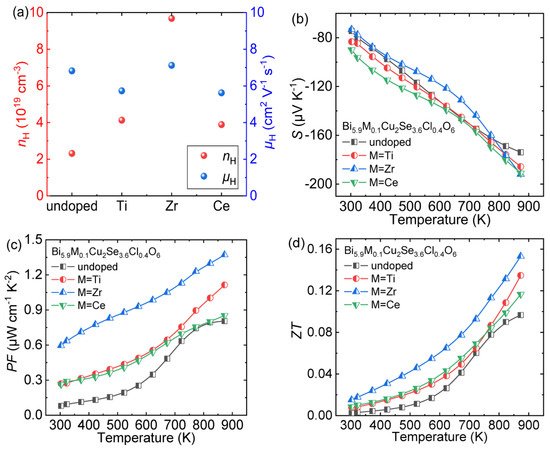
Zheng et al. chose Bi 6Cu 2Se 3.6 Cl 0.4 O 6 as the matrix and doped transition metal elements (Zr, Ti and Ce) at Bi sites to enhance its thermoelectric performance [43][30]. The introduction of transition metal elements can effectively increase the carrier concentration ( n H ) and maintain the carrier mobility ( μ H ; Figure 7 11 a), thereby optimizing the electric conductivity ( σ ) of the matrix. The S of all doped samples remains negative throughout the entire temperature range, indicating the stable n -type semiconductor properties ( Figure 7 11 b). Thanks to the optimized σ and maintained S , the power factor ( PF ) is effectively enhanced ( Figure 711 c). Finally, due to the enhanced electrical transport properties and reduced thermal conductivity [43][30], the peak ZT value reached ~0.16 at 873 K in Bi 5.9 Zr 0.1 Cu 2Se 3.6 Cl 0.4 O 6 ( Figure 711 d), which is 60% higher than that in Bi 6Cu 2Se 3.6 Cl 0.4 O 6 (~0.10 at 873 K).
As a new type of layered oxyselenide thermoelectric material, Bi 6Cu 2Se 4O 6 maintains the advantages of BiCuSeO and Bi 2O 2Se, such as lower-cost and nontoxic elements, better thermal and chemical stability. Moreover, Bi 6Cu 2Se 4O 6 can exhibit stable n -type semiconductor behavior by simple halogen doping and has intrinsic low thermal conductivity due to complex crystal structure. Thereby, Bi 6Cu 2Se 4O 6 is a new kind of n -type layered oxyselenide thermoelectric material with broad development prospects.