Integrated optical phased arrays (OPAs) can be used for beam shaping and steering with a small footprint, lightweight, high mechanical stability, low price, and high-yield, benefiting from the mature CMOS-compatible fabrication.
- integrated
- optical phased arrays
- beam shaping
- beam steering
1. Introduction
In recent years, optical phased arrays (OPAs) have attracted a great deal of attention. At optical wavelengths, small diffraction angles for a given aperture size can be achieved, compared with microwave radar systems. Featured by precise and agile free-space beam forming and steering [1][2][3][4][5][6][7][8][9][10][11][12], OPA techniques are highly desirable. However, current commercially available OPA components are mainly based on mechanical control, such as motor-driven rotating collimation stages/mirrors. Mechanical beam steering provides high efficiency and a relatively large scanning angle, through mechanically moving parts such as a gimbal, which can be susceptible to mechanical wear and tear, less stable, and limited in speed [13][14] due to the masses involved. The bulky mechanical steering approach is less preferred as it typically degrades in performance due to acceleration, temperature, vibration, and inertial forces. Additionally, mechanical steering often consumes significant energy. Furthermore, they require a complex assembly and calibration process, causing a greatly high unit cost. More importantly, these mechanical approaches are only capable of steering a single light beam. Arbitrary pointing and rapid steering as needed for advanced communication and sensing applications then become difficult or even incapable [14][15][16][17][18][19].
As one of the promising solutions for the next-generation dynamic beam steering, integrated OPAs simultaneously possess the advantages of being stable, rapid, and precise without relying on any mechanical motion, making them robust and insensitive to external constraints such as accelerations. Some of the integrated OPAs are presented in Figure 1. A wire-bonded device on a chip carrier plugged into a breadboard is presented in Figure 1a. Figure 1b shows a one-dimensional 64-channel chip-scale blue light phased array. A kind of III-V/Si phase-shifter-based OPA is shown in Figure 1c. Figure 1d is the photo of a fabricated OPA chip on a penny. Using an integrated approach, the OPAs can be made very small.
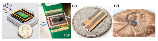
Figure 1. Integrated OPAs. (a) The wire-bonded device on the chip carrier plugged into the breadboard. Reprinted with permission from [20] © The Optical Society. (b) Blue light OPA. Reprinted with permission from [21] © The Optical Society. (c) A set of three 32-channel and one 240-channel OPAs on a coin. Reprinted with permission from the author of [22] published on Arxiv, 2018. (d) A photo of an OPA on a penny. Reprinted with permission from [23] © The Optical Society.
2. Principles
2.1. Fraunhofer Diffraction Model
TIn recent years, optical phased arrays (OPAs) have attracted a great deal of attention. At optical wavelengths, small diffraction angle Fraunhofer diffras for a given aperture size can be achieved, compared with microwave radar systems. Featured by precise and agile free-space beam forming and steering [1,2,3,4,5,6,7,8,9,10,11,12], OPA techniques are highly desirable. However, currention theor commercially available OPA components are mainly based on mechanical control, such as motor-driven rotating collimation stages/mirrors. Mechanical beam steering provides high efficiency [24]and a relatively large scanning angle, through mechanically moving parts such as a gimbal, which can be sused tceptible to mechanical wear and tear, less stable, and limited in speed [13,14] due to the masses involvedescribe the far-field interference . The bulky mechanical steering approach is less preferred as it typically degrades in performance due to acceleration, temperature, vibration, and inertial forces. Additionally, mechanical steering often consumes significant energy. Furthermore, they require a complex assembly and calibration process, causing a greatly high unit cost. More importantly, these mechanical approaches are only capable of steering a single light beam. Arbitrary pointing and rapid steering as needed for advanced communication and sensing applications then become difficult or even incapable [14,15,16,17,18,19].
As one of OPAs, in which scalar f the promising solutions for the next-generation dynamic beam steering, integrated OPAs simultaneously possess the advantages of being stable, rapid, and precise without relying on any mechanical motion, making them robust and insensitive to external constraints such as accelerations. Some of the integrated OPAs are presented in Figure 1. A wire-bonded device on a chip carrier pldugged into a breadboard is epresented in tFigure 1a. Figure 1b shows a one-dimensional x0y064-channel chiplane -scale blue light phased array. A kind of III-V/Si phase-shifter-based OPA is shown in Figure 1c. Figure 1d iffracts s the photo of a fabricated OPA chip on a penny. Using an integrated approach, the OPAs can be made very small.
Figure 1. Integrated OPAs. (a) The wire-bonded thedevice on the chip x1y1-carrier plugged into the breane dboard. Reprinted with permission from [40] © The Optical Society. (b) aBlue large disight OPA. Reprinted with permission from [41] © The Opticancel Society. (c) z0A [13],set ofollowing the r three 32-channel and one 240-channel OPAs on a coin. Reprinted with permission from the author of [42] puble bished on Arxiv, 2018. (d) A photo of an OPA on a penny. Reprinted with permission from [43] © The Opticalow: Society.
2. Principles
2.1. Fraunhofer Diffraction Model

wFigure 2. (a) Schermatic of an OPA based kon WGAs. Repris the frnted with permission from [13], © Gent Unive-rsity. (b) An OPA based on EF structures. Repace wavroduced from [18] published vectorby De Gruyter, 2016.
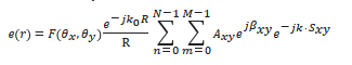
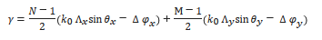
In Foprinciple, the Nfar-field radiation ×pattern Mof OPAs presented inis calculated by the far field of individual Figure 2antenna, multiplied by the far array factor [10,58,59]. The far-field at a certaipattern can be desirably modulated based on this theory.
2.2. Multi-Slit Diffraction Model

Figure 3. (a) Half-wavelength element pointspacing rOPA wis the far-field th integrated TO heaters for beam steering from left to right. Reproduced from [61] with the permission of AIP Publishing. (b) Schematic view of tern of one elemhe cross section of a WGA. Reprinted with permission from [8] © Then Opt, i.e.,ical Society. F (θx, θyc), multiplied by the sum of all the Schematic image of the proposed 2D beam steering device at a fixed wavelength. Reprinted with permission from [62] © The Optical Society. (d) Schemase ftic of a serpentine OPA. Reprinted with permission from [63] © The Optical Soctiety. (e) A 2 × 2 OPA receiver. Reprinted with permission frsom [43] © The Optical [13]:Society.
2.3. Beam Steering Based on WGAs
wNearly all there proposed R2D OPAs till =now |r|,depend Axyon iWGAs the . Not all the 2D OPAs’ far-field amplitude,patterns are completely formed by phase differences. There βxyare is the reome other steering approaches.
3. Building Blocks
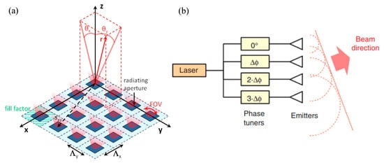
Integrated photonics paves the way for low-cost large-scale OPA chips. As presented in Figure 4, typically, there are four necessary parts in an OPA: laser source, beam splitters, phase shifters, and emitters [12], for efficient light generation, manipulation, and chip-to-free-space transmission. We will discuss each part in detail in this section. Then a brief overview about overlayers and buried oxide (BOX) layers is given. The optimized thicknesses of the overlayers and BOX layers enhance the upward radiation of WGAs.
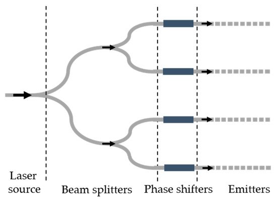
Figure 4. A typical integrated OPA structure.
4. Configurations
In terms of emitter types, OPAs can be sorted into EF OPAs, WGA-based OPAs, and OPAs based on other emitter structures.
4.1. EF OPAs
Typically, EF OPAs cativn only be tuned by the phase at eachdifference between adjacent elements. As presented in Figure 7a, k0the fis the freerst experimentally demonstrated aperiodic OPA was implemented on SOI [9]. The 12-channel unequal space wad OPA with a silica (SiO2) overlay veand individual TO phase shifters enabled an FOV of 31.9° at 1.55 μm [9].
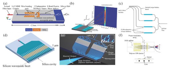
Figure 7. EF OPA structour,es. (a) A SOI-bansed EF OPA. Reproduced Sxyfrom [9] wisth the positiermission of tAIP Publishing. (b) The firadiating elemst demonstrated half-wavelength spacing OPA. Reproduced from [61] with the permissiont of AIP Publishing. θx(c) A dispersion-engineered handlf-wavelength EF OPA with low θycrosstalk. Reprindicate the angted with permission from the author of [94] publishe ofd on Arxiv, 2018. (d) A xSOI-based andEF OPA with a y-dSireO2 cavition, respectively. For uniform y for envelope tailoring. Reprinted with permission from [59] © The Opticarrl Society. (e) A 1D 64-chaysnnel blue [13],OPA withe far field is:
w sparse aperiodic spacing. Reprinted with permission from [41] © The γOptical Socis aety. (f) pSchase factor determinematic of a 16-channel polymer EF OPA. Reprinted with permission from [98] © Thed Optical bSociety.
4.2. WGA-Based OPAs
where Λx and Λy are the element spacing along the x- and y-axis, respectively. Δφx and Δφy are the phase differences.
Figure 2. (a) Schematic of an OPA based on WGAs. Reprinted with permission from [13], © Gent University. (b) An OPA based on EF structures. Reproduced from [18] published by De Gruyter, 2016.
In principle, the far-field radiation pattern of OPAs is calculated by the far field of individual antenna multiplied by the array factor [10][25][26]. The far-field pattern can be desirably modulated based on this theory.
2.2. Multi-Slit Diffraction Model
The first OPA introduced in Si photonics was illustramplemented based on WGA structures, as presented in Figure 2b,Figure 8a. uniformThe 1D EF OPAs can be described by the multi-slit diffraction model16-element WGA-based OPA was fabricated on the SOI platform. An FOV of 2.3° × 14.1° was demonstrated with both TO phase modulation and wavelength tuning [7]. ThA 4 × 4 WGA-base EF OPA is regarded as a rd OPA with an FOV of 1.5° was subsequently realized by the same group (Figure 8b). Waveclength tangular aperture uning based on grating dispersion was exploited to decrease the number of phase controls [8]. The achieved FOV of 1.5° is rray in the diffraction model. Then the far-field angular intensity distributioelatively narrow due to the small fill factor of the OPA, which can be further improved by redesigning OPA with a proper fill factor. An 8 × 8 WGA-based OPA with Si heaters presented in [13][26][27]Figure 8c isenabled in the form of:
wan FOV of 6° × 6° and a beamwidth of 1.6° × 1.6°. Lightly dopered δxSi waveguis the element size of thedes, which provided considerable resistances and low optical losses, and heavily N-doped Si lement OPA,ads were used I0as heaterstands for the unitary peak intensity in the far field of a single element, to drop most of the heating power on waveguides. Zigzagged Si lead structures were used to increase the heating length and θxto provindicates the angle ofde thermal isolations between waveguides and x-dirmetal ction. The identicalontacts. The measured TO efficiency was about 8.5 mW per π phase difshift [58].
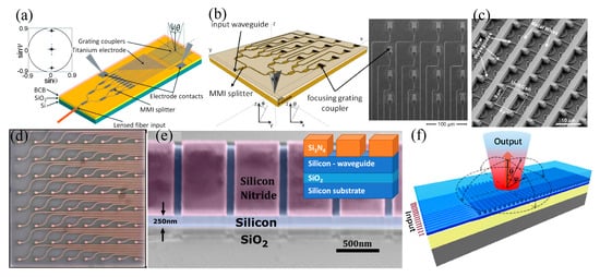
Figure 8. WGA-based OPAs. (a) The feirence of Δφxst OPA introduced in Si photonis applied between adjaccs. Reprinted with permission from [7] © Then Opt channels placedical Society. (b) A 4 × 4 WGA-bat a pitch of Λx.sed OPA. Reprinted with permission from [8] © The Optical Society. (c) SEFM of a fabricated OPAs are commonly used to achi after dry etching away the dielectric SiO2. Revprinte 1D beam formd with permission from [87] © The Optical Society. (d) Ang 8 × 8 OPA receiver. and steeringReprinted with permission from [43] © The Optical bSociety ph. (e) False-shifcolored tilted SEM of an aperiodic Si/Si3N4 grating. between waveguides.Reprinted with permission from [109] As© shown in Figure 3The Optica,l tSociety. (f) A heigh first fabricatcontrast WGA-based OPA with a half-wavelength elemhigh efficiency and low crosstalk. Reprinted with permission from [110] © Thent spaciOptical Society.
5. Material Platforms
Integ is used torated OPAs demonstrate beam steering over a range of 64° byd on photonics platforms enable low-cost chip-scale applications. In addition to conventional Si platforms, OPAs have been implemented on other photonic integrated thermo-optic (TO) heaterplatforms. The major platforms of integrated OPAs, which include Si photonics platforms, III/V platforms, and III–V/Si hybrid platforms.
7. Performances
The main easured intensity of the horizontal cross sections and stitched-together captured images are presented at the top and the bottom [28]valuation parameters of OPAs, which are FOVs, beamwidths and sidelobe suppression, modulation speeds, power consumption. It is important to note that one of critical factors determining FOVs, beamwidths and sidelobe suppression is the crosstalk and suppression among arrayed waveguide channels, and the efforts paid to reduce it should be reviewed first. For high-performance applications, large-scale OPAs are necessary. The scalability of OPAs will also be discussed. Finally, the calibration of OPAs to compensate for fabrication errors and mitigate crosstalk will be shown.
Figure 3. (a) Half-wavelength element spacing OPA with integrated TO heaters for beam steering from left to right. Reproduced from [28] with the permission of AIP Publishing. (b) Schematic view of the cross section of a WGA. Reprinted with permission from [8] © The Optical Society. (c) Schematic image of the proposed 2D beam steering device at a fixed wavelength. Reprinted with permission from [29] © The Optical Society. (d) Schematic of a serpentine OPA. Reprinted with permission from [30] © The Optical Society. (e) A 2 × 2 OPA receiver. Reprinted with permission from [23] © The Optical Society.
2.3. Beam Steering Based on WGAs
Nearly all the proposed 2D OPAs till now depend on WGAs. Not all the 2D OPAs’ far-field patterns are completely formed by phase differences. There are some other steering approaches.
3. Building Blocks
Integrated photonics paves the way for low-cost large-scale OPA chips. As presented in Figure 4, typically, there are four necessary parts in an OPA: laser source, beam splitters, phase shifters, and emitters [12], for efficient light generation, manipulation, and chip-to-free-space transmission. We will discuss each part in detail in this section. Then a brief overview about overlayers and buried oxide (BOX) layers is given. The optimized thicknesses of the overlayers and BOX layers enhance the upward radiation of WGAs.
Figure 4. A typical integrated OPA structure.
4. Configurations
In terms of emitter types, OPAs can be sorted into EF OPAs, WGA-based OPAs, and OPAs based on other emitter structures.
4.1. EF OPAs
Typically, EF OPAs can only be tuned by the phase difference between adjacent elements. As presented in Figure 5a, the first experimentally demonstrated aperiodic OPA was implemented on SOI [9]. The 12-channel unequal spaced OPA with a silica (SiO2) overlay and individual TO phase shifters enabled an FOV of 31.9° at 1.55 μm [9].
Figure 5. EF OPA structures. (a) A SOI-based EF OPA. Reproduced from [9] with the permission of AIP Publishing. (b) The first demonstrated half-wavelength spacing OPA. Reproduced from [28] with the permission of AIP Publishing. (c) A dispersion-engineered half-wavelength EF OPA with low crosstalk. Reprinted with permission from the author of [31] published on Arxiv, 2018. (d) A SOI-based EF OPA with a SiO2 cavity for envelope tailoring. Reprinted with permission from [26] © The Optical Society. (e) A 1D 64-channel blue OPA with sparse aperiodic spacing. Reprinted with permission from [21] © The Optical Society. (f) Schematic of a 16-channel polymer EF OPA. Reprinted with permission from [32] © The Optical Society.
4.2. WGA-Based OPAs
The first OPA introduced in Si photonics was implemented based on WGA structures, as presented in Figure 6a. The 1D 16-element WGA-based OPA was fabricated on the SOI platform. An FOV of 2.3° × 14.1° was demonstrated with both TO phase modulation and wavelength tuning [7]. A 4 × 4 WGA-based OPA with an FOV of 1.5° was subsequently realized by the same group (Figure 6b). Wavelength tuning based on grating dispersion was exploited to decrease the number of phase controls [8]. The achieved FOV of 1.5° is relatively narrow due to the small fill factor of the OPA, which can be further improved by redesigning OPA with a proper fill factor. An 8 × 8 WGA-based OPA with Si heaters presented in Figure 6c enabled an FOV of 6° × 6° and a beamwidth of 1.6° × 1.6°. Lightly doped Si waveguides, which provided considerable resistances and low optical losses, and heavily doped Si leads were used as heaters to drop most of the heating power on waveguides. Zigzagged Si lead structures were used to increase the heating length and to provide thermal isolations between waveguides and metal contacts. The measured TO efficiency was about 8.5 mW per π phase shift [25].
Figure 6. WGA-based OPAs. (a) The first OPA introduced in Si photonics. Reprinted with permission from [7] © The Optical Society. (b) A 4 × 4 WGA-based OPA. Reprinted with permission from [8] © The Optical Society. (c) SEM of a fabricated OPA after dry etching away the dielectric SiO2. Reprinted with permission from [33] © The Optical Society. (d) An 8 × 8 OPA receiver. Reprinted with permission from [23] © The Optical Society. (e) False-colored tilted SEM of an aperiodic Si/Si3N4 grating. Reprinted with permission from [34] © The Optical Society. (f) A high contrast WGA-based OPA with high efficiency and low crosstalk. Reprinted with permission from [35] © The Optical Society.
5. Material Platforms
Integrated OPAs demonstrated on photonics platforms enable low-cost chip-scale applications. In addition to conventional Si platforms, OPAs have been implemented on other photonic integrated platforms. The major platforms of integrated OPAs, which include Si photonics platforms, III/V platforms, and III–V/Si hybrid platforms.
6. Performances
The main evaluation parameters of OPAs, which are FOVs, beamwidths and sidelobe suppression, modulation speeds, power consumption. It is important to note that one of critical factors determining FOVs, beamwidths and sidelobe suppression is the crosstalk and suppression among arrayed waveguide channels, and the efforts paid to reduce it should be reviewed first. For high-performance applications, large-scale OPAs are necessary. The scalability of OPAs will also be discussed. Finally, the calibration of OPAs to compensate for fabrication errors and mitigate crosstalk will be shown.
79. Outlook
More applications can be achieved based on integrated OPAs. Monolithically integrated OPAs take advantage of full integration and small chip sizes. EF OPAs can be used for 1D beam forming and steering. Wavelength-tuned 1D long-WGA-based OPAs with phase modulations decrease steering complexities in 2D steering. Problems of expensive precisely tunable laser sources [11][36] and limited performance [37][38] could be solved. Simplified high-performance on-chip tunable lasers are highly desirable. Large-scale sparse aperiodic 2D OPAs, which have wide FOVs and narrow beamwidths, are promising candidates for high-performance OPA-based applications. Design complexity of large-scale sparse aperiodic 2D OPAs need to be decreased for further applications. A two-chip integrated OPA with a sparse aperiodic aperture might be a promising solution [36].
More applications can be achieved based on integrated OPAs. Monolithically integrated OPAs take advantage of full integration and small chip sizes. EF OPAs can be used for 1D beam forming and steering. Wavelength-tuned 1D long-WGA-based OPAs with phase modulations decrease steering complexities in 2D steering. Problems of expensive precisely tunable laser sources [11,45] and limited performance [64,84] could be solved. Simplified high-performance on-chip tunable lasers are highly desirable. Large-scale sparse aperiodic 2D OPAs, which have wide FOVs and narrow beamwidths, are promising candidates for high-performance OPA-based applications. Design complexity of large-scale sparse aperiodic 2D OPAs need to be decreased for further applications. A two-chip integrated OPA with a sparse aperiodic aperture might be a promising solution [45].
For applications based on precise beam forming and steering, WGAs with normal direction radiation [37][39] as well as structures with plateau envelops [26][39][40] can be highly desirable Modulation speeds are greatly enhanced by EO phase shifters based on the carrier density changing function. Monolithically integrated LiNbO
For applications based on precise beam forming and steering, WGAs with normal direction radiation [64,113] as well as structures with plateau envelops [59,113,118] can be highly desirable Modulation speeds are greatly enhanced by EO phase shifters based on the carrier density changing function. Monolithically integrated LiNbO
3 EO phase shifters [41] and contact graphene heaters with high efficiencies and operation speeds, low power consumption [42] can be used for excellent EO modulations. To decrease optical losses of sharp waveguide bends, 45° angle placed antennas may be used to enable optical routing through two sides of the aperture [36]. Fabrication errors need to be carefully treated [43].
EO phase shifters [105] and contact graphene heaters with high efficiencies and operation speeds, low power consumption [75] can be used for excellent EO modulations. To decrease optical losses of sharp waveguide bends, 45° angle placed antennas may be used to enable optical routing through two sides of the aperture [45]. Fabrication errors need to be carefully treated [142].