Metamaterials are the major type of artificially engineered materials which exhibit naturally unobtainable properties according to how their microarchitectures are engineered. Owing to their unique and controllable effective properties, including electric permittivity and magnetic permeability, the metamaterials play a vital role in the development of meta-devices.
1. Metamaterials
In Greek, the word meta means “beyond”. The metamaterials are new class of engineered materials which exhibit unusual electromagnetic properties that do not occur in natural materials. In general, natural materials like diamond, glass, etc., have positive refractive index, magnetic permeability, and electrical permittivity. Whereas these new engineered materials show negative index of refraction, negative electrical permittivity, and magnetic susceptibility. The metamaterials are also called as left-handed (LH) materials or backward wave (BW) media or negative index materials (NIM) or double negative (DNG) media. In addition, metamaterials have some special properties such as perfect lensing [1], classical electromagnetically induced transparency [2][3][4][5], cloaking capability [6], high frequency magnetism [7], dynamic modulation of Terahertz (THz) radiation [8], reverse Doppler effect, and reverse Cerenkov effect [9]. These unique properties of metamaterials enable them to fabricate functional devices with switching and tuning capabilities [10][11][12][13][14]. Further, based on the permittivity and the permeability, the metamaterials are categorized as mu-negative material (MNG), epsilon negative material (ENG), double positive material (DPS), and double negative material (DNG) [15]. The MNG and ENG are also called as single negative materials. Whereas the double negative and double positive materials can be engineered at particular frequency band. In the year 1968, Victor Veselago, who is a Russian physicist, first theoretically proposed the metamaterials [16]. He theoretically explored the electrodynamics of the materials with negative values of the magnetic permeability (μ) and relative permittivity (ɛ). Moreover, the propagation of electromagnetic waves is discussed in those materials. Nevertheless Smith et al. practically demonstrated for first time a structure which exhibits negative refraction in the microwave region [15]. In addition, J.B. Pendry et al. [17] fabricated the first metamaterial by two interpenetrating subsystems. Particularly, by using an array of thin metallic (copper) wires and rings, they fabricated split ring resonators (SRRs), which provide negative values of permittivity and permeability [17][18][19]. In metamaterials, the split rings play the role of atoms in natural materials and act as electrically small resonant particles which contribute negative permeability. Herein, copper wire contributes negative permittivity. Combined array exhibits negative permeability and permittivity.
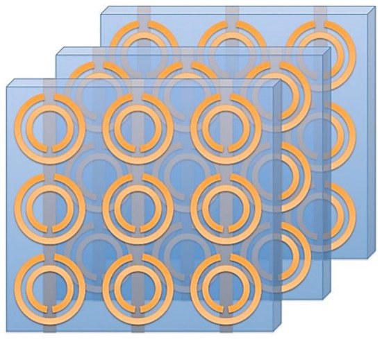
In Greek, the word meta means “beyond”. The metamaterials are new class of engineered materials which exhibit unusual electromagnetic properties that do not occur in natural materials. In general, natural materials like diamond, glass, etc., have positive refractive index, magnetic permeability, and electrical permittivity. Whereas these new engineered materials show negative index of refraction, negative electrical permittivity, and magnetic susceptibility. The metamaterials are also called as left-handed (LH) materials or backward wave (BW) media or negative index materials (NIM) or double negative (DNG) media. In addition, metamaterials have some special properties such as perfect lensing [1], classical electromagnetically induced transparency [2,3,4,5], cloaking capability [6], high frequency magnetism [7], dynamic modulation of Terahertz (THz) radiation [8], reverse Doppler effect, and reverse Cerenkov effect [9]. These unique properties of metamaterials enable them to fabricate functional devices with switching and tuning capabilities [10,11,12,13,14]. Further, based on the permittivity and the permeability, the metamaterials are categorized as mu-negative material (MNG), epsilon negative material (ENG), double positive material (DPS), and double negative material (DNG) [15]. The MNG and ENG are also called as single negative materials. Whereas the double negative and double positive materials can be engineered at particular frequency band. In the year 1968, Victor Veselago, who is a Russian physicist, first theoretically proposed the metamaterials [16]. He theoretically explored the electrodynamics of the materials with negative values of the magnetic permeability (μ) and relative permittivity (ɛ). Moreover, the propagation of electromagnetic waves is discussed in those materials. Nevertheless Smith et al. practically demonstrated for first time a structure which exhibits negative refraction in the microwave region [15]. In addition, J.B. Pendry et al. [17] fabricated the first metamaterial by two interpenetrating subsystems. Particularly, by using an array of thin metallic (copper) wires and rings, they fabricated split ring resonators (SRRs), which provide negative values of permittivity and permeability [17,18,19]. In metamaterials, the split rings play the role of atoms in natural materials and act as electrically small resonant particles which contribute negative permeability. Herein, copper wire contributes negative permittivity. Combined array exhibits negative permeability and permittivity. gives the pictorial representation of a metamaterial [20] (Figure taken from ref [20]). Later, Ziolkowski [21] reported another metamaterial which consists of substrate entrenched with capacitively loaded strips (CLSs) and square SRRs. In this material, capacitively loaded strips gives a strong response to electric fields and gives negative ɛ and SRRs interacts with magnetic fields and provides negative μ. Afterwards, numerous researchers designed and fabricated different metamaterials by using different methods like shadow mask/etching, clean room etching, etc., in many frequency bands. In addition, based on the presence of SRRs, the metamaterials are available in various forms. That means the metamaterials consisting SRRs are available in one, two, and three dimensions [22][23][24][25]. Further, those metamaterials without SRRs (for example, fishnet structure) are available in two, quasi-two, and three dimensions [26][27][28][29]. Hence, owing to their unique properties and structures, the metamaterials find their applications in various devices such as sensors [30][31][32], superlens [33], antennas [34][35], superconductors [36], absorbers [37][38][39][40][41][42], energy harvesting [43][44], etc. In this article, we have concentrated on recently developed metamaterials and their applications.
gives the pictorial representation of a metamaterial [20] (Figure taken from ref [20]). Later, Ziolkowski [21] reported another metamaterial which consists of substrate entrenched with capacitively loaded strips (CLSs) and square SRRs. In this material, capacitively loaded strips gives a strong response to electric fields and gives negative ɛ and SRRs interacts with magnetic fields and provides negative μ. Afterwards, numerous researchers designed and fabricated different metamaterials by using different methods like shadow mask/etching, clean room etching, etc., in many frequency bands. In addition, based on the presence of SRRs, the metamaterials are available in various forms. That means the metamaterials consisting SRRs are available in one, two, and three dimensions [22,23,24,25]. Further, those metamaterials without SRRs (for example, fishnet structure) are available in two, quasi-two, and three dimensions [26,27,28,29]. Hence, owing to their unique properties and structures, the metamaterials find their applications in various devices such as sensors [30,31,32], superlens [33], antennas [34,35], superconductors [36], absorbers [37,38,39,40,41,42], energy harvesting [43,44], etc. In this article, we have concentrated on recently developed metamaterials and their applications.
Figure 1. Pictorial representation of a metamaterial
[20].
2. Applications of Metamaterials
As we know, the metamaterials are engineered metamaterials which exhibit exceptional properties that cannot be found naturally. In metamaterials, the resonant nature of the atoms leads to the enhancement in light matter interaction that affords dramatic changes in the light properties [45]. Especially, chiral metamaterials give strong response to light, this chiroptical response surpasses the natural materials. Owing to these special properties, the chiral meta devices have potential applications in polarization sensitive nano optical devices [46][47]. For instance, 3D nanoarchitecture generally exhibit chiroptical response [48][49], which are widely used for fast polarization switching [50]. Compared to bulk materials, the metamaterials or metasurfaces show domination in controlling the amplitude, phase, and polarization of light. In recent years, researchers have concentrated on achieving strong chiroptical responses in metasurfaces by breaking the rotational symmetries at unit cell level [51][52][53][54][55]. In this regard, 2D patterned layer of chiral metamirrors present a decent light matter interaction [53][54]. In addition, the metal/dielectric/metal sandwich structures display improved chiroptical responses. Recently, Kang et al. [56] demonstrated an ultrathin nonlinear chiral meta mirror. The proposed metamirror consists an array of SRRs made up of amorphous silicon (α-Si). They reported that the metamirror exhibit fast optical polarization switching (picosecond) of near infrared light at pump energies of picojoule per resonator. This can be achieved by strong chiroptic response of the atoms in the proposed mirror. Hence the chiral metamirrors are promising candidates for power efficient and high-speed polarization state modulators in optical information processing.
As we know, the metamaterials are engineered metamaterials which exhibit exceptional properties that cannot be found naturally. In metamaterials, the resonant nature of the atoms leads to the enhancement in light matter interaction that affords dramatic changes in the light properties [45]. Especially, chiral metamaterials give strong response to light, this chiroptical response surpasses the natural materials. Owing to these special properties, the chiral meta devices have potential applications in polarization sensitive nano optical devices [46,47]. For instance, 3D nanoarchitecture generally exhibit chiroptical response [48,49], which are widely used for fast polarization switching [50]. Compared to bulk materials, the metamaterials or metasurfaces show domination in controlling the amplitude, phase, and polarization of light. In recent years, researchers have concentrated on achieving strong chiroptical responses in metasurfaces by breaking the rotational symmetries at unit cell level [51,52,53,54,55]. In this regard, 2D patterned layer of chiral metamirrors present a decent light matter interaction [53,54]. In addition, the metal/dielectric/metal sandwich structures display improved chiroptical responses. Recently, Kang et al. [56] demonstrated an ultrathin nonlinear chiral meta mirror. The proposed metamirror consists an array of SRRs made up of amorphous silicon (α-Si). They reported that the metamirror exhibit fast optical polarization switching (picosecond) of near infrared light at pump energies of picojoule per resonator. This can be achieved by strong chiroptic response of the atoms in the proposed mirror. Hence the chiral metamirrors are promising candidates for power efficient and high-speed polarization state modulators in optical information processing.
Further, it is important to guide the waves for reliable transportation of information through a physical channel. But, due to attenuation and back-scattering, the transportation of energy is sensitive to sharp turns and defects in high frequency systems such as signal processing [57][58]. However, in matter systems topological phenomenon is considered for unidirectional and attenuation free energy transportation [59]. Moreover, the topological metamaterials can transport the energy effectively, which is called phononic energy transportation. Till now, the mechanical metamaterials are being used in large scale systems such as gyroscopic lattices [60][61], arrays of pendulums [62][63], structured plates [64], and so on. For utilizing the mechanical materials in high frequency energy transportation, the metamaterial topological systems must be scaled on to the chip level [65][66]. In this view, Cha et al. [67] proposed topological nanoelectromechanical metamaterials. The proposed metamaterials consist of 2D array of free-standing SiN nanomembranes which can operate at high frequencies of 10–20 MHz. They also demonstrated the presence of edge states and frequency dispersion. Finally, the proposed on-chip topological metamaterials are suitable for high frequency signal processing applications.
Further, it is important to guide the waves for reliable transportation of information through a physical channel. But, due to attenuation and back-scattering, the transportation of energy is sensitive to sharp turns and defects in high frequency systems such as signal processing [57,58]. However, in matter systems topological phenomenon is considered for unidirectional and attenuation free energy transportation [59]. Moreover, the topological metamaterials can transport the energy effectively, which is called phononic energy transportation. Till now, the mechanical metamaterials are being used in large scale systems such as gyroscopic lattices [60,61], arrays of pendulums [62,63], structured plates [64], and so on. For utilizing the mechanical materials in high frequency energy transportation, the metamaterial topological systems must be scaled on to the chip level [65,66]. In this view, Cha et al. [67] proposed topological nanoelectromechanical metamaterials. The proposed metamaterials consist of 2D array of free-standing SiN nanomembranes which can operate at high frequencies of 10–20 MHz. They also demonstrated the presence of edge states and frequency dispersion. Finally, the proposed on-chip topological metamaterials are suitable for high frequency signal processing applications.
Furthermore, Cho et al. [68] proposed the concept of virtualized metamaterials to overcome the shortcomings of traditional metamaterials. Through engineered resonant modes with structured atoms the metamaterials permit to attain constitutive parameters beyond their natural range. Generally, the tunability of constitutive parameters in real time applications is a fundamental challenge in traditional metamaterials. This can overcome by the proposed concept of virtualized metamaterials. In addition, they reported that the replacement of the physical structure with designed fast signal processing Kernel circuit. The circuit allows exhibiting defined frequency dispersion through which one can control mass density and bulk modulus of the metamaterials. In addition, the proposed concept is helpful in designing topological, non-Hermitian, and non-reciprocal systems by tuning the frequency, dispersion, and amplitude for fast signal processing applications.
Afterwards, the fluorescent resonant energy transfer (FRET) [69][70] between the donor and acceptor enhances the efficiency of solar cells [71], organic light emitting diodes [72], photosynthesis [73], and so on. Nevertheless, in case of direct dipole–dipole interaction, the resonance energy transfer occurs only at very short distances of 10 nm, beyond this distance efficiency of the energy transfer decreases significantly. This is one of the major limitations of transportation of energy in solar cells. Continuous research efforts are going on to enhance the efficiency of the energy transportation by using hyperbolic metamaterials [74][75], plasmonic nanostructures [76][77], and planar silver films [78]. Especially, the optical topological transition (OTT) in a metamaterial theoretically considered the ideal model for the enhancing energy transfer over long range orders [79]. In this regard, recently Deshmukh et al. [80] demonstrated the long range (about 160 nm) direct energy transfer between the donor CdSe/ZnS core-shell quantum dots and acceptor Cy3 organic dye molecules by using OTT in a metamaterial. They reported that the metamaterial consists the alternating layers of germanium (Ge) deposited silver (Ag) and alumina (Al
Afterwards, the fluorescent resonant energy transfer (FRET) [69,70] between the donor and acceptor enhances the efficiency of solar cells [71], organic light emitting diodes [72], photosynthesis [73], and so on. Nevertheless, in case of direct dipole–dipole interaction, the resonance energy transfer occurs only at very short distances of 10 nm, beyond this distance efficiency of the energy transfer decreases significantly. This is one of the major limitations of transportation of energy in solar cells. Continuous research efforts are going on to enhance the efficiency of the energy transportation by using hyperbolic metamaterials [74,75], plasmonic nanostructures [76,77], and planar silver films [78]. Especially, the optical topological transition (OTT) in a metamaterial theoretically considered the ideal model for the enhancing energy transfer over long range orders [79]. In this regard, recently Deshmukh et al. [80] demonstrated the long range (about 160 nm) direct energy transfer between the donor CdSe/ZnS core-shell quantum dots and acceptor Cy3 organic dye molecules by using OTT in a metamaterial. They reported that the metamaterial consists the alternating layers of germanium (Ge) deposited silver (Ag) and alumina (Al 2
O
3
). The OTT in the metamaterial alters the density of states between donor and acceptor, which leads to the long-range energy transfer with 32% transfer efficiency. Further the experimental values are in good agreement with theoretical values. Finally, they concluded that the OTT in metamaterials enhances the efficiency of energy transportation and controls the transfer process. Owing to this, the OTT in metamaterials have potential applications in numerous fields such as organic solar cells, quantum entanglement, etc.
In addition, the hyperbolic metamaterials are also gained considerable attention. A hyperbolic metamaterial is a special type of anisotropic metamaterial whose isofrequency contour (IFC) takes the form of an open hyperboloid because the principal components of its electric or magnetic tensor have opposite signs [81][82][83][84]. The unusual nature of IFC enables the hyperbolic metamaterials to be used for controlling the electromagnetic waves in new ways. Through controlling the shape of the hyperbolic dispersion, one can flexibly control the propagation of light in hyperbolic metamaterial, resulting abnormal scattering [85][86][87][88] splitting [89][90][91], all angle negative refraction [92][93][94][95][96], etc. These hyperbolic metamaterials are also called indefinite media [97][98] or polaritonic crystal in which the coupled states of matter and light give rise to a larger bulk density of electromagnetic states [99][100]. Owing to this, hyperbolic metamaterial possesses strong enhancement of spontaneous emission [101][102][103][104][105] and Cherenkov emission with low energy electrons [106][107][108][109]. These hyperbolic metamaterials can be used in multifunctional platform for sensing, quantum engineering, waveguiding, super resolution imaging, and so on [110][111]. At first, the hyperbolic nature of metamaterial is first observed in microwave region. The natural as well as engineered material exhibits the hyperbolic dispersion. In infrared and visible region, some natural materials such as SiC, graphite, Bi
In addition, the hyperbolic metamaterials are also gained considerable attention. A hyperbolic metamaterial is a special type of anisotropic metamaterial whose isofrequency contour (IFC) takes the form of an open hyperboloid because the principal components of its electric or magnetic tensor have opposite signs [81,82,83,84]. The unusual nature of IFC enables the hyperbolic metamaterials to be used for controlling the electromagnetic waves in new ways. Through controlling the shape of the hyperbolic dispersion, one can flexibly control the propagation of light in hyperbolic metamaterial, resulting abnormal scattering [85,86,87,88] splitting [89,90,91], all angle negative refraction [92,93,94,95,96], etc. These hyperbolic metamaterials are also called indefinite media [97,98] or polaritonic crystal in which the coupled states of matter and light give rise to a larger bulk density of electromagnetic states [99,100]. Owing to this, hyperbolic metamaterial possesses strong enhancement of spontaneous emission [101,102,103,104,105] and Cherenkov emission with low energy electrons [106,107,108,109]. These hyperbolic metamaterials can be used in multifunctional platform for sensing, quantum engineering, waveguiding, super resolution imaging, and so on [110,111]. At first, the hyperbolic nature of metamaterial is first observed in microwave region. The natural as well as engineered material exhibits the hyperbolic dispersion. In infrared and visible region, some natural materials such as SiC, graphite, Bi 2
Se
3, etc., exhibit the hyperbolic dispersion due to excitation of phonon polaritons [112][113][114][115][116][117][118]. Similarly, the engineered structures such as multilayer fishnets [119], uniaxial metasurfaces [120][121], and metal-dielectric structures [122][123] have subwavelength unit cells that display the hyperbolic dispersion. The dispersion manipulation in hyperbolic metamaterials can be used in many applications like sub-diffraction imaging [124], sub-wavelength modes [125], thermal emission engineering [126][127][128], high sensitivity sensors, hyper lens, etc. Therefore, the hyperbolic metamaterials with unusual properties will play a significant role in the advancement of novel optical devices in future. Recently, Schoche et al. [129] reported the behaviour of tunable hyperbolic metamaterials which are derived from self-assembled carbon nanotubes. To obtain the hyperbolic metamaterials from carbon nanotubes, they employed the Muller matrix ellipsometry over the broad spectral range from mid-IR to UV region to specify the dielectric tensor function on high dense films consisting single wall carbon nanotubes. Optically these films are anisotropic and act as metamaterials with effective medium response. Further, an oscillator model developed from the proposed metamaterials exhibit broad range of hyperbolic dispersion compared to film consisting unordered carbon nanotubes. Hence, the aligned carbon nanotubes form the metamaterial and play a prominent role in accomplishing tunable hyperbolic nature.
, etc., exhibit the hyperbolic dispersion due to excitation of phonon polaritons [112,113,114,115,116,117,118]. Similarly, the engineered structures such as multilayer fishnets [119], uniaxial metasurfaces [120,121], and metal-dielectric structures [122,123] have subwavelength unit cells that display the hyperbolic dispersion. The dispersion manipulation in hyperbolic metamaterials can be used in many applications like sub-diffraction imaging [124], sub-wavelength modes [125], thermal emission engineering [126,127,128], high sensitivity sensors, hyper lens, etc. Therefore, the hyperbolic metamaterials with unusual properties will play a significant role in the advancement of novel optical devices in future. Recently, Schoche et al. [129] reported the behaviour of tunable hyperbolic metamaterials which are derived from self-assembled carbon nanotubes. To obtain the hyperbolic metamaterials from carbon nanotubes, they employed the Muller matrix ellipsometry over the broad spectral range from mid-IR to UV region to specify the dielectric tensor function on high dense films consisting single wall carbon nanotubes. Optically these films are anisotropic and act as metamaterials with effective medium response. Further, an oscillator model developed from the proposed metamaterials exhibit broad range of hyperbolic dispersion compared to film consisting unordered carbon nanotubes. Hence, the aligned carbon nanotubes form the metamaterial and play a prominent role in accomplishing tunable hyperbolic nature.
In addition, with the help of face-to-face SRRs and a central bar Hu et al. [130] demonstrated the design of tunable terahertz metamaterial (TTM) for switching applications. They reported that, the free spectrum ranges (FSR) of TTM varies bi-directionally, i.e., broadened, and shortened with respect to variation of gap between SSR and central bar. In TE mode, FSR is broadened by 0.14 THz (from 0.65 to 0.79 THz), whereas in TM mode it is shortened by 0.19 THz (from 0.30 to 0.19 THz). Moreover, TTM shows the dependence of polarization when it is subjected to external electromagnetic radiation. Moreover, in both single band and dual band proposed TTM acts like switch at TE mode, whereas at TM mode, the resonance of TTM insensitive to the displacement of central bar. Owing to this the proposed TTM can be utilized as switch in terahertz frequency range.
Li and Cheng [131] proposed a temperature tunable metamaterial absorber (MMA) by using two stacked square shaped strontium titanate resonator structures (STOs) and copper substrate. From the analysis of simulation studies, they reported that, at specific frequencies, i.e., 0.114 THz and 0.181 THz in terahertz region the reflectance of the proposed MMA is about 2.1% and 0.2% at room temperature. Moreover, it has maximum absorption peaks 97.9 and 99.8% at the same frequencies. In addition, owing to symmetry of unit cell structure STO based MMA shows polarization insensitive nature to both transverse electric and transverse magnetic modes. Further, the distribution studies of power flow and electromagnetic fields disclosed that, the excitations of fundamental dipole modes in the MMA are the origin of the high level of absorption. In addition, the absorbance of the proposed MMA can be altered by varying the external temperature and, by varying its structural parameters. Owing to the excellent characteristics, the proposed STO-based MMA may have potential prospects in thermal imaging, temperature sensing, thermal emission, etc. In addition, scientists designed strontium titanate (STO) based single band tunable metamaterial absorber [131]. They reported that, with respect to structural parameters, absorption peak is increased and resonant frequency is reduced. This means the absorption peaks are enhanced from 90 to 99.4%, whereas the resonant frequency is shifted from 6.2 to 5.8 THz. As the temperature is increased from 300 to 380 K the absorption peak shows 2% decrement. While the resonant frequency shifted from 6.2 to 7.1 THz. So, the proposed metamaterial can be tuned by temperature. Moreover, the temperature tunable metamaterial exhibits the excellent absorption property.
Next, using four L-shaped anisotropic metamaterials Lu et al. [132] demonstrated an ultrathin reflective linear polarization converter. The proposed design can convert the linearly polarized radiation to cross polarized radiation with the conversion ratio of 98% from 4.2 to 5.2 THz. In addition, the reflection coefficient of cross polarization is greatly influenced by the deflection angles relative to y-axis [133]. So, the proposed metamaterial-based device can be useful for the manipulation of polarization in optical instruments. In recent years, planar metamaterials are studied extensively owing to their potential applications in design of lasing spacers, flat optical components, nonlinear devices, etc. In these metamaterials high Q-factor (quality factor) is essen26GH26tial for enabling strong light-matter coupling [134][135]. In this regard, the Fano resonances support the narrow linewidths with high Q-factor values [136][137][138]. The Fano resonance in metasurfaces is originated from increased electric field in the subwavelength capacitive gaps of symmetry broken resonators. Earlier the Fano resonance is modulated by changing the coupling distance in the unit cell or changing the asymmetry parameters of the unit cell [139][140][141]. But, in this technique the Fano resonance works in passive mode. Therefore, the researchers searched for an alternative design for active control of metasurfaces. They suggested that active control is possible by controlling the conductivity of the Fano structure. Until now, very less work has been done on the Fano structures [142][143][144][145]. In this connection, Ma et al. [146] demonstrated an active switching of extremely large Q-factor Fano resonance by using VO
Next, using four L-shaped anisotropic metamaterials Lu et al. [132] demonstrated an ultrathin reflective linear polarization converter. The proposed design can convert the linearly polarized radiation to cross polarized radiation with the conversion ratio of 98% from 4.2 to 5.2 THz. In addition, the reflection coefficient of cross polarization is greatly influenced by the deflection angles relative to y-axis [133]. So, the proposed metamaterial-based device can be useful for the manipulation of polarization in optical instruments. In recent years, planar metamaterials are studied extensively owing to their potential applications in design of lasing spacers, flat optical components, nonlinear devices, etc. In these metamaterials high Q-factor (quality factor) is essen26GH26tial for enabling strong light-matter coupling [134,135]. In this regard, the Fano resonances support the narrow linewidths with high Q-factor values [136,137,138]. The Fano resonance in metasurfaces is originated from increased electric field in the subwavelength capacitive gaps of symmetry broken resonators. Earlier the Fano resonance is modulated by changing the coupling distance in the unit cell or changing the asymmetry parameters of the unit cell [139,140,141]. But, in this technique the Fano resonance works in passive mode. Therefore, the researchers searched for an alternative design for active control of metasurfaces. They suggested that active control is possible by controlling the conductivity of the Fano structure. Until now, very less work has been done on the Fano structures [142,143,144,145]. In this connection, Ma et al. [146] demonstrated an active switching of extremely large Q-factor Fano resonance by using VO 2
(vanadium oxide)-implanted THz asymmetric double C-shaped metamaterial structures. They reported that the double Fano resonances are highly sensitive to the temperatures and, the Fano resonances can be switched at low thermal pumping of 68 °C. The exited Fano resonances in the metadevices can be completely vanished by cooling. However, the tuning of Fano resonances in cooling and heating are different. To understand the internal mechanism of the temperature tuned Fano resonances, at respective resonant frequencies they simulated the distributions of surface current and electric field for high (70 °C) and low (45 °C) temperatures. In addition, at 1.16 THz, the resonant linewidth of the proposed device is 0.015 THz, and the Q-factor is 98, which is very high compared to traditional metamaterials. Hence, the proposed temperature tunable Fano resonant devices are promising candidates for designing advanced high-performance photonic devices like ultrasensitive temperature sensors. Later, Li et al. [147] reported an active Fano metasurfaces with the help of graphene-based terahertz asymmetric split-ring resonant structure (Gr-TASR) on silicon (Si) substrate. The active control in the proposed design is possible through controlling the conductivity of the graphene by a combination of CW (continuous wave) illumination and bias voltage. Further, they experimentally observed that, the clear modulation of Fano resonance is achieved by optical illumination with 0.7 Wcm −2
power density at very low voltage of about −0.8 V. This may be due to shorting effect between the capacitive split gaps of Gr-TASR. This is an effective approach for controlling the metamaterials actively with both electrical and optical fields which can play a prominent role in designing of variety of futuristic graphene-silicon based terahertz photonic devices.
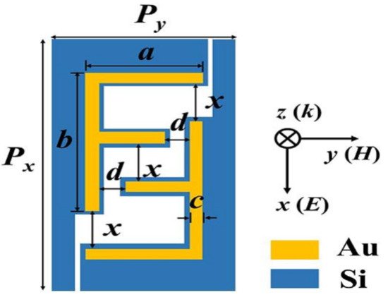
Further, Lin et al. [148] demonstrated the design of a tunable terahertz (THz) resonator by using AFSM (asymmetrical F-shaped metamaterial) which is composed of Au-layer fabricated on SOI (silicon-on-insulator) substrate. shows the schematic representation of the proposed F-shaped THz resonator (
of Ref. [148]). Without changing the other parameters, they designed three F-shaped resonators of lengths 60 μm, 65 μm, and 70 μm. When the proposed resonator is exposed to electromagnetic radiation, it shows the switch function for single band resonance at TM mode and dual band resonance at TE mode. Owing to this one can use the proposed device as a THz switch in TE-mode and as a THz filter in TM-mode. In addition, the tuning resonances are in between 0.2 and 0.4 THz in TE-mode and the resonator having length of 60 μm exhibits largest Q-factor of 40. Moreover, at TM-mode, all the proposed resonators show same Q-factor of 20. All the outcomes are evinced that the proposed AFSM device is suitable for designing environmental sensor. They reported that, the proposed device is subjected to surrounding environmental factors with different refractive indices for further enhancement of the flexibility and efficiency. Therefore, this new AFSM device provides a way to enhance the sensitivity of metamaterials in THz region for polarizer, sensor, and switching applications.
Figure 2. Schematic representation of the F-shaped THz resonator ( of Ref.
[148]).