Your browser does not fully support modern features. Please upgrade for a smoother experience.
Please note this is a comparison between Version 1 by Ya Yang and Version 2 by Catherine Yang.
Low-temperature cooling possesses advantages in applicability, stability and nondamaging characteristics. Because of the temperature-related physical properties of nanoscale materials.
- temperature dependence
- photoelectric
1. Introduction
To meet the emergent requirement of the development of sustainable and clean energy, solar energy, recognized as the best potential alternative to fossil-fuel power, has been intensively investigated regarding its effective harvesting, conversion and storage in past decades [1][2][3][4][5][6][7][8][9][1,2,3,4,5,6,7,8,9]. One of the major developments lies in the mature utilization of nanoscale materials, such as two-dimensional materials [10][11][10,11] and quantum dots [12]. However, the advent of the photoelectric device also raises concerns regarding adaptivity to diversified environments, such as outer space or other extreme environments. Differing from the widely researched performance at normal temperature condition, the investigations on extreme temperature conditions, especially low temperature, are insufficient for completing the underlying physical mechanism and applying it to practical use. There are a handful of reports showing decreased performance at low temperature. These weakening phenomena caused by lowering temperature are ascribed to many causes including frozen carrier diffusion [13], reduced absorption [14], interfacial ion accumulation [15], phase transition [16] and radiative [17] and nonradiative [18] recombination. However, there are also many reports that low-temperature operation is not a restriction but an enhancement to overall photoelectric performance, ranging from low-dimension materials to nanocrystals. The effectiveness of the cooling method on these devices not only provides a strategy for constructing photoelectric devices under extreme conditions but also reveals the potential of cooling as an innovative and efficacious method for improving optoelectronic performance. It is worth noting that small drops in temperature will also cause visible improvement in photoelectric performance [19][20][21][19,20,21]. No matter the need, in applications or in theoretical research, relevant reports on the cooling method is in urgent need of systematic summary and guidance.
To realize improvements through low-temperature cooling, the underlying function mechanism deserves investigation. Similar to coupling effects or surface modification [22][23][24][25][26][22,23,24,25,26], the cooling method functions without changing composition or inherent structures. Moreover, compared with these traditional methods, cooling’s enhanced effects have unique advantages in applicability, stability and nondestructive characteristics. In view of the existing theories, the general temperature-dependent methods can be divided into three aspects: materials, devices and performances, shown in Figure 1. Temperature variation first directly functions on materials, inducing fluctuations in energy level [27][28][29][27,28,29], carrier motions [30], density of traps/carriers [31] and crystal structure transition [32]. For cooling-enhanced materials, regulation in energy levels causes changes in absorption [28], barrier height [33] and so on [34][35][34,35], then influences photon absorption and charge transportation. Some intrinsic characteristics of carriers are reported to show huge enhancement from cooling, including mobility [36], diffusion length [37] and corresponding densities [38]. For specific materials, structure transition [39] has been observed in a low-temperature range, providing more potential for cooling regulation. When the above phenomena integrated with devices, the cooling-enhanced properties in devices can be classified into absorption [40], carrier diffusion and recombination [41][42][41,42], resistance [43], photoconductivity [44], permittivity [45], interfaces and defects [46] and can improve the overall performance of both photodetectors and solar cells. The full mechanism is based on temperature-dependent optical and electrical properties, thus the emergence of the utilization of the cooling method, which possesses many advantages over conventional improvement methods and also possesses benefits to reliable photoelectric application in harsh environments.
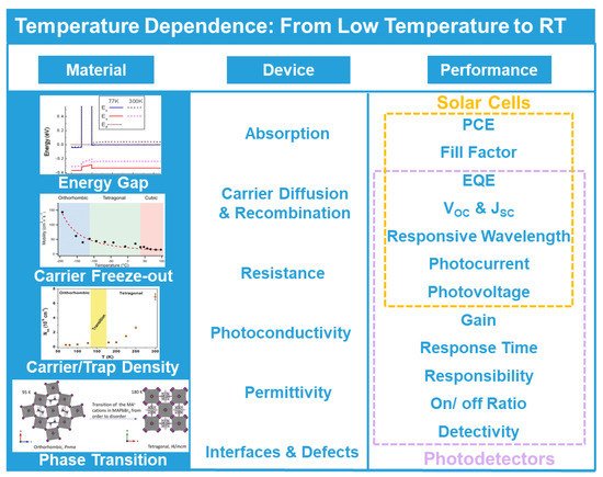
Figure 1. Temperature-dependent effect on photoelectric devices including materials, devices and performances. All images reproduced with permission: “Bandgap” (adapted from [29], with permission from the American Institute of Physics, 2014). “Carrier freeze-out” (adapted from [30], with permission from Wiley-VCH, 2015). “Carrier/Trap Density” (adapted from [31], with permission from Wiley-VCH, 2017). “Phase Transition” (adapted from [32], with permission from Wiley-VCH, 2018).
2. Applications of the Low-Temperature-Enhanced Photoelectric Process
Advances in cooling-enhanced photoelectronic processes bring new opportunities to conventional photoelectrical nanomaterials, based on superiority in tuneable band alignment, suppressed noise current, a different mechanism of charge motion and so on, hence, enabling more innovative optoelectronic applications. The cooling method has been widely used in the photodetection field, especially for background-limited infrared photodetectors. As shown in Figure 28(a1), summarised by Wang et al., typical high-resolution photodetectors in the infrared field are dominated by materials with low-temperature operating requirements [47][143]. In addition to reduced dark current at cryogenic temperatures, significant enhanced detectivity makes the cooling method a more effective strategy for realizing highly sensitive photodetection. As shown, for example, by Figure 28(a2,a3), the III-V group photodetector acquires accuracy to distinguish details such as vessels when the temperature further drops to 60 K [48][66]. Despite difficulties in operation at extremely low temperature, the negative relationship between the temperature and the photoresponse of the discussed materials provides feasibility in greatly increasing devices’ performance using the proper cooling process. In contrast to the mature application of cooling in photodetection, solar cells possessing complex configuration and integrated optoelectrical mechanisms are in the beginning stage. Recently, Chen et al. successfully fabricated an unencapsulated perovskite device exhibiting higher performance in a simulated near-space (especially low-temperature) environment [49][181]. The enhancement at low temperature mainly originates from the self-elimination of intrinsic defects brought by phase transition under a cooling environment. As illustrated in Figure 8b, when temperatures decrease from 300 K to 220 K, the phase transition from cubic to tetragonal structure eliminates these intrinsic point defects then causes PCE to increase to 25.2% at 220 K. Previous discussion also lists the utilization of the frozen hysteresis effect at suitable temperature to improve the conversion efficiency of perovskite solar cells. Further investigations are expected to demonstrate the enormous advantages of cooling-enhanced solar cells, especially perovskite in space, near polar regions and other cool conditions. Integrated optoelectronic effects with other sensing functions play an important role in next-generation communication, healthcare, bioelectronics and so on [23][50][51][52][53][54][55][56][57][58][59][60][61][23,182,183,184,185,186,187,188,189,190,191,192,193]. In 2020, Chang et al. investigated the low-temperature cooling-enhanced pryo-phototronic effect on SnS/CdS photodetectors, depicted in Figure 28(c1,c2). For this planar structure photodetector, significant enhancement (~500%) of the ratio of pyroelectric to total signal was achieved as temperature declined to 77 K [62][194]. Further research on ZnO/perovskite [63][195] and p-Si/n-ZnO [64][196] verified that low temperature improved the coupling effect phenomenon. The coupling mechanism was unveiled by Ma et al. with experiments on BaTiO3 [65][197], shown in Figure 28(c3,c4). Under low-temperature operation, shallow trap levels play a more important role in photoinduced response. At room temperature, the function of shallow traps has been suppressed. However, the temperature dependence of piezo-photoelectric effect showed that cooling weakens piezoelectric and photoelectric performance [66][67][198,199]; these results remain a puzzle in the investigation of photoelectricity-evolved coupling mechanisms at low temperature. More multifunctional detectors operating at low temperature deserve investigation, especially those based on low-temperature-enhancing mechanisms. Another challenge for cooling operations is the limit of difficulties in realizing extremely low temperatures. According to specific temperature-dependent effects of optoelectronic devices, it is recommended to lock in optimal performance by cooling to the proper temperature rather than extreme low temperature. For the negative temperature-dependent section, even slightly cooler temperature will cause invisible improvement. In this regard, we believe that investigations on cooling-enhanced performance will make breakthroughs in low-temperature photoelectric application and push forward research on temperature-regulated optoelectrical mechanisms.
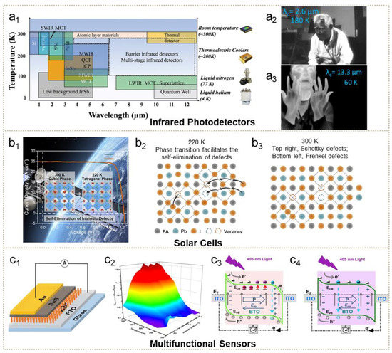
Figure 28. Applications of the low-temperature cooling method for photoelectric devices. (a) Cooling application in infrared photodetectors. (a1) Summary of working temperature for infrared photodetectors (adapted from [47][143], with permission from Wiley-VCH, 2019). (a2,a3) Temperature-dependent sensing performance of infrared photodetectors (adapted from [48][66], with permission from the Multidisciplinary Digital Publishing Institute, 2020). (b) Cooling application in solar cells (adapted from [49][181], with permission from Elsevier, 2020). (c) Cooling application in multifunction sensors. (c1,c2) Cooling-enhanced pyro-photoelectric coupling effect (adapted from [62][194], with permission from Wiley-VCH, 2020). (c3,c4) The underlying cooling-enhanced mechanism of the coupling effect (adapted from [65][197], with permission from Elsevier, 2019).