In recent years, high-performance photodetectors have attracted wide attention because of their important applications including imaging, spectroscopy, fiber-optic communications, remote control, chemical/biological sensing and so on. Nanostructured perovskites are extremely suitable for detective applications with their long carrier lifetime, high carrier mobility, facile synthesis, and beneficial to device miniaturization. Because the structure of the device and the dimension of nanostructured perovskite have a profound impact on the performance of photodetector, we divide nanostructured perovskite into 2D, 1D, and 0D, and review their applications in photodetector (including photoconductor, phototransistor, and photodiode), respectively. The devices exhibit high performance with high photoresponsivity, large external quantum efficiency (EQE), large gain, high detectivity, and fast response time. The intriguing properties suggest that nanostructured perovskites have a great potential in photodetection.
- nanostructured perovskites
- high-performance photodetector
- different dimensions
Note: The following contents are extract from your paper. The entry will be online only after author check and submit it.
1. Introduction
Photodetectors—the vital components of modern imaging and communication systems—have been playing an increasingly important role in modern industrial production, basic scientific research, space development, ocean exploration, military and national defense, environmental protection, medical diagnosis, transportation, and other fields. For example, ultraviolet photodetectors can be used in ozone sensing, flame sensing, etc. [1][2][3]. The visible photodetectors can be used in biological sensing, video imaging, and convert communications [4][5][6][7]. Infrared photodetectors can be used as infrared night vision. [8][9][10] The THz photodetectors can be used in the security detection of customs, airports, and other special occasions [11][12][13]. Therefore, the further research of photodetectors is of great significance. A semiconductor, which is essential for a photodetector, can absorb the incident photons and generate electron and hole pairs. In the presence of a built-in or applied electric field, electric current is generated when the electrodes extracted and collected photogenerated carriers. In order to obtain a high-performance photodetector with high sensitivity and fast response, the semiconductor needs to have effective charge collection, low trap state density, and high carrier mobility. Till now, a large variety of semiconductor materials have been used for constructing photodetectors, including Si [14][15][16], carbon nanotubes [17][18], group II–VI and III–V compounds [19][20][21], and remarkable progress has been made in improving the detection performance. Epitaxial growth technology with stringent conditions, which is the most commonly used for synthesis, hampers their commercial application [22]. Therefore, it is of great significance to exploit candidates to reduce production cost and improve photodetector performance.
Recently, perovskites with a typical formula of ABX
has attracted wide research interest in the photodetector field [23][24][25]. For ABX
, A is a monovalent cation (CH
NH
(MA), Cs
, etc.), B is the divalent metal cation (Pb
, Sn
, etc.), and X is a halide ion (Br
, Cl
and I
). Many properties of perovskite make it an ideal material for photodetectors. For example, ambipolar transport, low density of defects and traps within bandgap can effectively reduce the charge recombination, and thus improve the performance of photodetectors. [26] The absorption spectra can cover the UV–Visible–Infrared region by facile halide substitution, which is desirable for broadband photodetector applications [27][28]. High absorption coefficient and direct bandgap result in a fast photoresponse in a very thin perovskite layer because of short transmission distance of photongenerated carriers [29][30]. In addition, low cost and easy preparation remove obstacles in future mass preparation. For example, MAPbI
film-based photodetectors with a metal–semiconductor–metal (MSM) structure exhibited a broad photoresponse range from 310 nm to 780 nm, with a photoresponsivity of 3.49 A W
and external quantum efficiency (EQE) of 1.19 × 10
% [31]. However, there is an inherent paradox to simultaneously possess both low dark currents and high photocurrents. The former requires a large number of defects or barriers that appear in polycrystalline film to inhibit the transmission of thermally excited carriers [32][33][34], while the latter requires single crystals with good crystallinity for effective charge transfer [35][36][37]. Compared with photodetectors based on polycrystalline film and bulk crystals, nanostructured photodetectors exhibit superior performances. The large surface-to-volume ratios of nanostructures result in longer photocarrier lifetime, which is conducive to higher sensitivity and responsivity. In addition, the reduced dimension shortens the carrier transmission time and improves the response speed [19][38][39][40][41]. Therefore, the performance of photodetector based on nanostructured perovskites will be better. For example, a high responsivity of 1294 A W
with a ultrahigh detectivity of 2.6 × 10
Jones was obtained in α-CsPbI
nanowire-based photodetector [42]. In addition, an ultrahigh response speed (19/25 µs) was obtained in a photodetector based on atom-thin 2D CsPbBr
nanosheets [43]. An ultrahigh EQE over 10
% was demonstrated by a phototransistor based on CsPbI
Br
quantum dots (QDs)/monolayer MoS
heterostructure [44]. All these are enough to show that the photodetectors based on nanostructured perovskites have more advantages in ultrahigh responsivity and ultrafast response speed. There have been some reviews on nanostructured perovskite-based photodetectors. Gu et al. [45] focus on the effect of elemental composition and dimensionality of the perovskite materials on photodetector performance. Wang et al. [46] systematically summarized the synthesis, optoelectronic properties, and performance of photodetectors based on low-dimensional perovskites. Here, more emphasis is placed on the effect of the device structure and the dimension of nanostructured perovskites on the device performance.
The key parameters of photodetectors are shown in
.
The key parameters of photodetectors.
| Parameters | Definition |
|---|---|
| Photoresponsivity (R) | the ratio of the photocurrent to the incident power on the active area: R = (Ip − Id)/(PA), where Ip is the photocurrent, Id is the dark current, P is the light intensity, A is the active area |
| EQE | Photoelectric conversion efficiency. EQE = Rhc/e, where h is the Planck’s constant, c is the light velocity, e is the electronic charge. |
| Gain (G) | The number of charge carriers through external circuit for per incident photon: G = τl/τt = τl(µV)/d2, where τl is the carrier lifetime, τt is the carrier transit time, µ is the carrier mobility, V is bias voltage, d is the channel length |
| Detectivity (D*) | D* = (A△ f)1/2/NEP, where A is the active area of the detector, △f is the electrical bandwidth, NEP is the noise equivalent power. |
| LDR | LDR usually stands for “Linear Dynamic Range”, defined as the range in which the current response of the photodetector is linearly proportional to the light intensity. LDR = 20 log (Ip*/Id), Where Id is the dark current. |
| Response speed (rise/decay time) | The ability of devices to track the incident light signal. |
2. Photodetectors
Perovskite-based photodetector devices can be divided into two categories, photovoltaic and photoconductive photodetectors. According to the spatial layout of the photoactive medium and electrodes, perovskite-based photodetector devices can be further divided into vertical type and lateral type. In general, vertical photodetectors provide fast response and low driving voltage because of the small electrode spacing with a short carrier transit length; in contrast, lateral photodetectors show slow response and high driving voltage due to their large electrode spacing. For photovoltaic photodetector, or photodiode (
a), the device structure is similar to that of solar cell configuration. Photodiodes based on perovskite polycrystalline films or single crystals are widely reported, but those based on nanostructured perovskites are rarely reported. Photodiodes typically rely on PN junction, which can provide a built-in electrical field at the junction interface to aid the electrons and holes to transport in opposite directions toward electrodes. Owing to the junction barrier at the interface, photodiodes exhibit low dark current and large detectivity. However, they suffer from low responsivity and external quantum efficiency (EQE ≤ 100%). As for photoconductive photodetector, it can be further divided into photoconductor (
b) and phototransistor (
c). Compared with photovoltaic photodetector, photoconductive photodetector exhibits high responsivity, EQE (beyond 100%) and large gain. External voltage leading to multiple electrical carriers recycling per single incident photon should be responsible for the large gain [47][48][49][50]. However, large gain, in turn, usually results in a slow response speed because both the response time and the gain are determined by the carrier lifetime. Therefore, the intrinsic contradictions between the responsivity and response speed always exist. One solution is to fabricate phototransistor by adding gate electrode (Si) and dielectric layer (SiO
) to the photoconductor. The charge transport can be controlled by applying a gate voltage. It is demonstrated that phototransistor can simultaneously enhance the photoresponsivity and exhibit an ultrafast photoresponse speed [51].
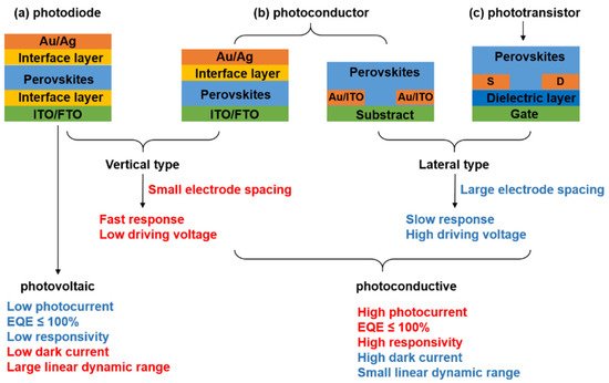
Schematic and characteristics of perovskite-based photodetectors. (
) photodiode, (
) photoconductor, and (
) phototransistor.
References
- Xu, Z.; Zhang, Y.; Wang, Z. ZnO-based photodetector: From photon detector to pyro-phototronic effect enhanced detector. J. Phys. D Appl. Phys. 2019, 52, 223001.
- Li, D.; Jiang, K.; Sun, X.; Guo, C. AlGaN photonics: Recent advances in materials and ultraviolet devices. Adv. Opt. Photonics 2018, 10, 43–110.
- Oh, S.; Kim, C.-K.; Kim, J. High responsivity β-Ga2O3 metal–semiconductor–metal solar-blind photodetectors with ultraviolet transparent graphene electrodes. Acs Photonics 2017, 5, 1123–1128.
- Qi, J.; Qiao, W.; Zhou, X.; Yang, D.; Zhang, J.; Ma, D.; Wang, Z.Y. High--Detectivity All--Polymer Photodetectors with Spectral Response from 300 to 1100 nm. Macromol. Chem. Phys. 2016, 217, 1683–1689.
- Luo, L.-B.; Yang, X.-B.; Liang, F.-X.; Jie, J.-S.; Li, Q.; Zhu, Z.-F.; Wu, C.-Y.; Yu, Y.-Q.; Wang, L. Transparent and flexible selenium nanobelt-based visible light photodetector. CrystEngComm 2012, 14, 1942–1947.
- Qiu, X.; Wang, Z.; Hou, X.; Yu, X.; Yang, D. Visible-blind short-wavelength infrared photodetector with high responsivity based on hyperdoped silicon. Photonics Res. 2019, 7, 351–358.
- Yu, P.; Hu, K.; Chen, H.; Zheng, L.; Fang, X. Novel p–p Heterojunctions Self-Powered Broadband Photodetectors with Ultrafast Speed and High Responsivity. Adv. Funct. Mater. 2017, 27, 1703166.
- Gong, F.; Fang, H.; Wang, P.; Su, M.; Li, Q.; Ho, J.C.; Chen, X.; Lu, W.; Liao, L.; Wang, J. Visible to near-infrared photodetectors based on MoS2 vertical Schottky junctions. Nanotechnology 2017, 28, 484002.
- Wang, L.; Jie, J.; Shao, Z.; Zhang, Q.; Zhang, X.; Wang, Y.; Sun, Z.; Lee, S.T. MoS2/Si heterojunction with vertically standing layered structure for ultrafast, high--detectivity, self--driven visible–near infrared photodetectors. Adv. Funct. Mater. 2015, 25, 2910–2919.
- Rogalski, A.; Antoszewski, J.; Faraone, L. Third-generation infrared photodetector arrays. J. Appl. Phys. 2009, 105, 4.
- Meledin, D.V.; Marrone, D.P.; Tong, C.-Y.; Gibson, H.; Blundell, R.; Paine, S.N.; Papa, D.C.; Smith, M.; Hunter, T.R.; Battat, J. A 1-THz superconducting hot-electron-bolometer receiver for astronomical observations. IEEE Trans. Microw. Theory Tech. 2004, 52, 2338–2343.
- Tong, C.-Y.; Meledin, D.V.; Marrone, D.P.; Paine, S.N.; Gibson, H.; Blundell, R. Near field vector beam measurements at 1 THz. IEEE Microw. Wirel. Compon. Lett. 2003, 13, 235–237.
- Mittleman, D.M. Twenty years of terahertz imaging. Opt. Express 2018, 26, 9417–9431.
- Zhang, H.; Zhang, X.; Liu, C.; Lee, S.-T.; Jie, J. High-responsivity, high-detectivity, ultrafast topological insulator Bi2Se3/silicon heterostructure broadband photodetectors. ACS Nano 2016, 10, 5113–5122.
- Xie, C.; Nie, B.; Zeng, L.; Liang, F.-X.; Wang, M.-Z.; Luo, L.; Feng, M.; Yu, Y.; Wu, C.-Y.; Wu, Y. Core–shell heterojunction of silicon nanowire arrays and carbon quantum dots for photovoltaic devices and self-driven photodetectors. ACS Nano 2014, 8, 4015–4022.
- Zhang, A.; Kim, H.; Cheng, J.; Lo, Y.-H. Ultrahigh responsivity visible and infrared detection using silicon nanowire phototransistors. Nano Lett. 2010, 10, 2117–2120.
- Barone, P.W.; Baik, S.; Heller, D.A.; Strano, M.S. Near-infrared optical sensors based on single-walled carbon nanotubes. Nat. Mater. 2005, 4, 86–92.
- Arnold, M.S.; Zimmerman, J.D.; Renshaw, C.K.; Xu, X.; Lunt, R.R.; Austin, C.M.; Forrest, S.R. Broad spectral response using carbon nanotube/organic semiconductor/C60 photodetectors. Nano Lett. 2009, 9, 3354–3358.
- Kind, H.; Yan, H.; Messer, B.; Law, M.; Yang, P. Nanowire ultraviolet photodetectors and optical switches. Adv. Mater. 2002, 14, 158–160.
- Jin, Y.; Wang, J.; Sun, B.; Blakesley, J.C.; Greenham, N.C. Solution-processed ultraviolet photodetectors based on colloidal ZnO nanoparticles. Nano Lett. 2008, 8, 1649–1653.
- Baeg, K.J.; Binda, M.; Natali, D.; Caironi, M.; Noh, Y.Y. Organic light detectors: Photodiodes and phototransistors. Adv. Mater. 2013, 25, 4267–4295.
- Herman, M.A.; Sitter, H. Molecular Beam Epitaxy: Fundamentals and Current Status; Springer: Berlin/Heidelber, Germany, 2012; Volume 7.
- Bao, C.; Zhu, W.; Yang, J.; Li, F.; Gu, S.; Wang, Y.; Yu, T.; Zhu, J.; Zhou, Y.; Zou, Z. Highly flexible self-powered organolead trihalide perovskite photodetectors with gold nanowire networks as transparent electrodes. ACS Appl. Mater. Interfaces 2016, 8, 23868–23875.
- Lin, Q.; Armin, A.; Burn, P.L.; Meredith, P. Filterless narrowband visible photodetectors. Nat. Photonics 2015, 9, 687–694.
- Maculan, G.; Sheikh, A.D.; Abdelhady, A.L.; Saidaminov, M.I.; Haque, M.A.; Murali, B.; Alarousu, E.; Mohammed, O.F.; Wu, T.; Bakr, O.M. CH3NH3PbCl3 single crystals: Inverse temperature crystallization and visible-blind UV-photodetector. J. Phys. Chem. Lett. 2015, 6, 3781–3786.
- Xing, G.; Mathews, N.; Sun, S.; Lim, S.S.; Lam, Y.M.; Grätzel, M.; Mhaisalkar, S.; Sum, T.C. Long-range balanced electron-and hole-transport lengths in organic-inorganic CH3NH3PbI3. Science 2013, 342, 344–347.
- Bekenstein, Y.; Koscher, B.A.; Eaton, S.W.; Yang, P.; Alivisatos, A.P. Highly Luminescent Colloidal Nanoplates of Perovskite Cesium Lead Halide and Their Oriented Assemblies. J. Am. Chem. Soc. 2015, 137, 16008–16011.
- Tong, Y.L.; Zhang, Y.W.; Ma, K.; Cheng, R.; Wang, F.; Chen, S. One-Step Synthesis of FA-Directing FAPbBr3 Perovskite Nanocrystals toward High-Performance Display. ACS Appl. Mater. Interfaces 2018, 10, 31603–31609.
- Takahashi, Y.; Hasegawa, H.; Takahashi, Y.; Inabe, T. Hall mobility in tin iodide perovskite CH3NH3SnI3: Evidence for a doped semiconductor. J. Solid State Chem. 2013, 205, 39–43.
- Yin, W.J.; Shi, T.; Yan, Y. Unique properties of halide perovskites as possible origins of the superior solar cell performance. Adv. Mater. 2014, 26, 4653–4658.
- Hu, X.; Zhang, X.; Liang, L.; Bao, J.; Li, S.; Yang, W.; Xie, Y. High-Performance Flexible Broadband Photodetector Based on Organolead Halide Perovskite. Adv. Funct. Mater. 2014, 24, 7373–7380.
- Saidaminov, M.I.; Adinolfi, V.; Comin, R.; Abdelhady, A.L.; Peng, W.; Dursun, I.; Yuan, M.; Hoogland, S.; Sargent, E.H.; Bakr, O.M. Planar-integrated single-crystalline perovskite photodetectors. Nature Commun. 2015, 6, 1–7.
- Fang, Y.; Dong, Q.; Shao, Y.; Yuan, Y.; Huang, J. Highly narrowband perovskite single-crystal photodetectors enabled by surface-charge recombination. Nat. Photonics 2015, 9, 679–686.
- Han, Q.; Bae, S.H.; Sun, P.; Hsieh, Y.T.; Yang, Y.; Rim, Y.S.; Zhao, H.; Chen, Q.; Shi, W.; Li, G. Single crystal formamidinium lead iodide (FAPbI3): Insight into the structural, optical, and electrical properties. Adv. Mater. 2016, 28, 2253–2258.
- Liu, X.; Gu, L.; Zhang, Q.; Wu, J.; Long, Y.; Fan, Z. All-printable band-edge modulated ZnO nanowire photodetectors with ultra-high detectivity. Nat. Commun. 2014, 5, 1–9.
- Wu, X.; Trinh, M.T.; Niesner, D.; Zhu, H.; Norman, Z.; Owen, J.S.; Yaffe, O.; Kudisch, B.J.; Zhu, X.-Y. Trap states in lead iodide perovskites. J. Am. Chem. Soc. 2015, 137, 2089–2096.
- De Quilettes, D.W.; Vorpahl, S.M.; Stranks, S.D.; Nagaoka, H.; Eperon, G.E.; Ziffer, M.E.; Snaith, H.J.; Ginger, D.S. Impact of microstructure on local carrier lifetime in perovskite solar cells. Science 2015, 348, 683–686.
- Soci, C.; Zhang, A.; Xiang, B.; Dayeh, S.A.; Aplin, D.; Park, J.; Bao, X.; Lo, Y.-H.; Wang, D. ZnO nanowire UV photodetectors with high internal gain. Nano Lett. 2007, 7, 1003–1009.
- McDonald, S.A.; Konstantatos, G.; Zhang, S.; Cyr, P.W.; Klem, E.J.; Levina, L.; Sargent, E.H. Solution-processed PbS quantum dot infrared photodetectors and photovoltaics. Nat. Mater. 2005, 4, 138–142.
- Fang, X.; Bando, Y.; Liao, M.; Gautam, U.K.; Zhi, C.; Dierre, B.; Liu, B.; Zhai, T.; Sekiguchi, T.; Koide, Y. Single--crystalline ZnS nanobelts as ultraviolet--light sensors. Adv. Mater. 2009, 21, 2034–2039.
- Huang, X.; Wang, M.; Willinger, M.-G.; Shao, L.; Su, D.S.; Meng, X.-M. Assembly of three-dimensional hetero-epitaxial ZnO/ZnS core/shell nanorod and single crystalline hollow ZnS nanotube arrays. ACS Nano 2012, 6, 7333–7339.
- Chen, G.; Feng, J.; Gao, H.; Zhao, Y.; Pi, Y.; Jiang, X.; Wu, Y.; Jiang, L. Stable α--CsPbI3 Perovskite Nanowire Arrays with Preferential Crystallographic Orientation for Highly Sensitive Photodetectors. Adv. Funct. Mater. 2019, 29, 1808741.
- Song, J.; Xu, L.; Li, J.; Xue, J.; Dong, Y.; Li, X.; Zeng, H. Monolayer and Few-Layer All-Inorganic Perovskites as a New Family of Two-Dimensional Semiconductors for Printable Optoelectronic Devices. Adv. Mater. 2016, 28, 4861–4869.
- Wu, H.; Si, H.; Zhang, Z.; Kang, Z.; Wu, P.; Zhou, L.; Zhang, S.; Zhang, Z.; Liao, Q.; Zhang, Y. All-Inorganic Perovskite Quantum Dot-Monolayer MoS2 Mixed-Dimensional van der Waals Heterostructure for Ultrasensitive Photodetector. Adv. Sci. 2018, 5, 1801219.
- Gu, H.; Chen, S.C.; Zheng, Q. Emerging Perovskite Materials with Different Nanostructures for Photodetectors. Adv. Opt. Mater. 2020, 2001637.
- Wang, H.P.; Li, S.; Liu, X.; Shi, Z.; Fang, X.; He, J.H. Low-Dimensional Metal Halide Perovskite Photodetectors. Adv. Mater. 2021, 33, e2003309.
- Song, J.; Cui, Q.; Li, J.; Xu, J.; Wang, Y.; Xu, L.; Xue, J.; Dong, Y.; Tian, T.; Sun, H.; et al. Ultralarge All-Inorganic Perovskite Bulk Single Crystal for High-Performance Visible-Infrared Dual-Modal Photodetectors. Adv. Opt. Mater. 2017, 5, 1700157.
- Liang, F.-X.; Wang, J.-Z.; Zhang, Z.-X.; Wang, Y.-Y.; Gao, Y.; Luo, L.-B. Broadband, Ultrafast, Self-Driven Photodetector Based on Cs-Doped FAPbI3 Perovskite Thin Film. Adv. Opt. Mater. 2017, 5, 1700654.
- Wang, F.; Mei, J.; Wang, Y.; Zhang, L.; Zhao, H.; Zhao, D. Fast Photoconductive Responses in Organometal Halide Perovskite Photodetectors. ACS Appl. Mater. Interfaces 2016, 8, 2840–2846.
- Li, Y.; Shi, Z.-F.; Li, S.; Lei, L.-Z.; Ji, H.-F.; Wu, D.; Xu, T.-T.; Tian, Y.-T.; Li, X.-J. High-performance perovskite photodetectors based on solution-processed all-inorganic CsPbBr3 thin films. J. Mater. Chem. 2017, 5, 8355–8360.
- Li, F.; Ma, C.; Wang, H.; Hu, W.; Yu, W.; Sheikh, A.D.; Wu, T. Ambipolar solution-processed hybrid perovskite phototransistors. Nat. Commun. 2015, 6.