The ongoing energy crisis and global warming caused by the massive usage of fossil fuels and emission of CO2 into atmosphere continue to motivate researchers to investigate possible solutions. The conversion of CO2 into value-added solar fuels by photocatalysts has been suggested as an intriguing solution to simultaneously mitigate global warming and provide a source of energy in an environmentally friendly manner. There has been considerable effort for nearly four decades investigating the performance of CO2 conversion by photocatalysts, much of which has focused on structure or materials modification. In particular, the application of low-dimensional structures for photocatalysts is a promising pathway. Depending on the materials and fabrication methods, low-dimensional nanomaterials can be formed in zero dimensional structures such as quantum dots, one-dimensional structures such as nanowires, nanotubes, nanobelts, and nanorods, and two-dimensional structures such as nanosheets and thin films. These nanostructures increase the effective surface area and possess unique electrical and optical properties, including the quantum confinement effect in semiconductors or the localized surface plasmon resonance effect in noble metals at the nanoscale.
- photocatalysis
- carbon dioxide conversion
- nanostructures
- low-dimensional photocatalysts
- solar fuels
1. Background
2
2
2
2
2
2
3
4
2
2
2
2
2
3
2
3
4), graphene, conjugated polymers, covalent organic framework, metal organic frameworks, metal chalcogenides, metal oxides, black phosphorus, bismuth-based materials, and perovskites [4][5][6][7][8][9][10][11][12][13][14]. Moreover, a variety of strategies and approaches have been applied to improve the photocatalyst performance through elemental doping, solid solution, heterostructure, nanostrucutralization, surface engineering and modification, crystal facet engineering, cocatalysts utilization, or dimensionality tailoring [15][16][17][18][19].
2 conversion, decreasing the dimensionality and constructing nanostructures of the photocatalyst have attracted a lot of attention owing to their favorable advantages in photocatalysis: first, nanostructured photocatalysts suppress the carrier recombination due to their higher crystallinity compared to non-nanostructured materials [20][21][22]; second, the implementation of low dimensionality modifies the electronic structure of bulk materials due to the quantum confinement effect in semiconductors or localized surface plasmon resonance effect in noble metals at the nanoscale; third, low-dimensional materials possess larger surface-area-to-volume ratio in comparison with bulk materials, providing more reaction sites. All three features can contribute to improved solar-driven catalytic reactions [19][23].
2. The Main Fundamentals of CO2 Photoconversion into Solar Fuels and Hydrocarbon Species
2.1. Nature of CO
2
2
2
2
2
2
+4
2
2
2
2
2
2.2. CO
2
Adsorption on the Surface of Photocatalysts
2
2
2 on several semiconductor photocatalysts has been investigated [26][27]. For instance, the adsorption of CO
2
2
2
2
2
2
2
2
COδ⋅−2
Figure 1: oxygen coordination, carbon coordination, and mixed coordination [24][28][29]. The beneficial feature of
COδ⋅−2
2
2
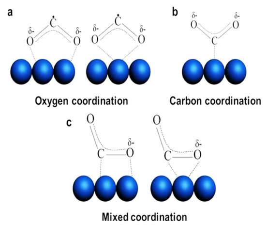
Figure 1.
2
2
Table 1, the solar fuel production is determined by the number of electrons and protons included in the reaction [20][24]. For example, two electrons are required for CO evolution, while methane production is an eight-electron reaction. The adsorption of CO
2
2
Table 1.
2
2O at 25 °C and atmospheric pressure [20][24].
| Reaction | Eo at pH 7 (V vs. NHE) |
Solar Fuel |
|---|
| CO2 reduction | CO2 + 2H+ + 2e− → CO + H2O | −0.51 | CO | |||||
| CO2 + 8H+ + 8e− → CH4 + 2H2O | −0.24 | CH4 | ||||||
| CO2 + 6H+ + 6e− → CH3OH + H2O | −0.39 | CH3OH | ||||||
| 2CO2 + 12H+ + 12e− → C2H5OH + 3H2O | −0.33 | C2H5OH | ||||||
| CO | 2 | + 2H | + | + 2e | − | → HCOOH | −0.58 | HCOOH |
| CO2 + 4H+ + 4e− → HCHO + H2O | ||||||||
| −0.48 | ||||||||
| HCHO | ||||||||
| H2O oxidation | ||||||||
| 2H | 2O → O2 +4H+ | |||||||
| +0.81 | ||||||||
| O | 2 | |||||||
2.3. The Mechanism of Efficient CO
2
Photoconversion
2
2
2
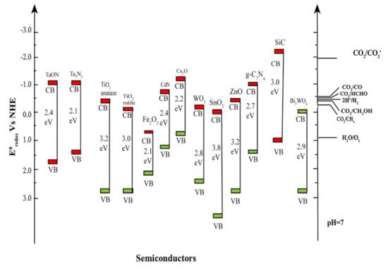
Figure 2.
2 reduction into solar fuels (Adapted from [31]).
g
2
2
2
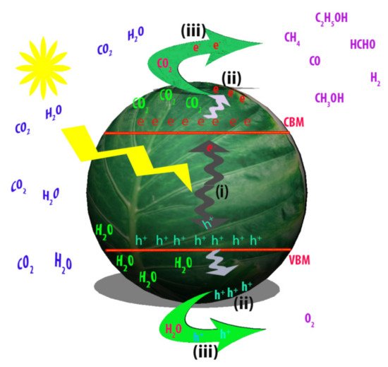
Figure 3.
2
i
ii
iii
2
2
3. Strategies for Enhancement in the Light-Driven CO2 Conversion over Low-Dimensional Photocatalysts
2
2
Table 2.
2
3
4
3
4
3
4
3
4
3
4
3
4
| Dimensionality | Morphology | Photocatalyst | Light Source | Reducing Agent | Main Product | Activity [µmol∙g−1∙h−1] |
Ref. |
|---|
| 0D | QD 3–12 nm |
CsPbBr3 | 300 W Xe lamp | H2O | CO CH4 |
4.26 1.53 |
[33][45] |
| QD 2.3 nm |
Cs3Bi2I9 | 300 W Xe lamp | H2O | CO | 1.15 | [34][46] | |
| QD 2.9 nm |
Cs3Bi2Br9 | 300 W Xe lamp | H2O | CO | 26.95 | ||
| QD 2.4 nm |
Cs3Bi2Cl9 | 300 W Xe lamp | H2O | CO | 21.01 | ||
| NC 9.5 nm |
Cs2AgBiBr6 | AM 1.5G | Ethyl acetate | CO CH4 |
2.35 1.6 |
[35][47] | |
| QD 9.45 nm |
FAPbBr3 | 300 W Xe arc lamp | H2O | CO CH4 |
181.25 16.9 |
[36][48] | |
| QD 5.86 nm |
GQD | 300 W Xe lamp 420 nm cutoff filter |
H2O | CH3OH | 0.695 | [11] | |
| 1D | NR | CeO2 | 300 W Xe lamp | H2O | CO | 0.020 | [37][49] |
| NT | TiO2 | 300 W Xe arc lamp 320 nm < λ < 780 nm |
H2O | CH4 | 2.128 | [21] | |
| NR | TiO2 | 300 W Xe arc lamp 320 nm < λ < 780 nm |
H2O | CH4 | 1.41 | [21] | |
| NT | P-g-C3N4 | 300 W Xe lamp | H2O/TEOA | CO CH4 |
2.37 1.81 |
[38][50] | |
| NT | PGCN | 300 W Xe lamp | H2O/MeCN /TEOA | CO | 103.6 | [39][51] | |
| NT | Bi12O17Cl2 | 300 W Xe lamp | H2O | CO | 48.6 | [40][52] | |
| NT | Bi12O17Br2 | 300 W Xe lamp | H2O | CO | 34.5 | [41][53] | |
| 2D | NS | g-C3N4 | 300 W Xe arc lamp | MeCN/TEOA (4:1) |
CO CH4 |
5.407 1.549 |
[42][54] |
| UTNS | g-C3N4 | 300 W Xe lamp | H2O | CH4 CH3OH |
1.39 1.87 |
[43][55] | |
| UTNS | SiC | 300 W Xe lamp | H2O | CO CH4 |
1.29 3.11 |
[44][56] | |
| UTNS | Bi2MoO6 | 300 W Xe lamp | H2O | CO | 3.62 | [45][57] | |
| 0D/1D | QD/NW | Black P/WO3 | 300 W Xenon arc lamp | H2O | CO C2H4 |
~ 135 ~ 11 |
[13] |
| QD (10 nm)/NT | WS2/Bi2S3 | 300 W Xe arc lamp | H2O | CH3OH C2H5OH |
9.55 6.95 |
[46][58] | |
| QD (3.5 nm)/NW | Ti3C2/Cu2O | 300 W Xe lamp | H2O | CH3OH | 78.50 | [47][59] | |
| 0D/2D | QD (1.6 nm)/NS | CuO/WO3 | 300 W Xe lamp λ > 400 nm |
H2O | CO | 1.58 | [48][60] |
| ND (4.4 nm)/NS | CND/p-CN | Xe arc lamp | H2O | CO CH4 |
5.88 2.92 |
[49][61] | |
| QD/NS | TiO2/g-C3N4 | 300 W Xe lamp λ > 400 nm |
MeCN/TEOA | CO | 77.8 | [50][62] | |
| QD (5nm)/NS | Au/TiO2 | 300 W Xe arc lamp | H2O | CO CH4 |
19.75 70.34 |
[51][63] | |
| QD (7nm) /NS | CsPbBr3/Bi2WO6 | 300 W Xe lamp λ > 400 nm |
H2O | CO/CH4 | 503 µmol∙ g−1 | [52][64] | |
| 1D/2D | NF/NS | TiO2/MoS2 | 350 W Xe lamp | H2O | CH4 CH3OH |
2.86 2.55 |
[53][65] |
| NT/NS | CNT/g-C3N4 | 200 W Hg and solar simulator | H2O | CO CH4 |
410 74 |
[54][66] | |
| NR/NS/NF | Au/TiO2/BiVO4 | 300 W Xe lamp | H2O | CO CH4 |
2.5 7.5 |
[55][67] | |
| 2D/2D | NS/NS | Ti3C2/Bi2WO6 | 300 W Xe lamp | H2O | CH4 CH3OH |
1.78 0.44 |
[56][68] |
| NS/NS | Bi2WO6/BiOI | 500 W Xe arc lamp λ < 400 nm |
H2O | CH4 | 2.92 | [57][69] | |
| NS/NS | Mt/m-CN | 35 W Xenon lamp | H2O/H2 | CO CH4 |
505 330 |
[58][70] | |
| NS/NS | SnS2/TiO2 | 300 W Xe lamp | H2O | CH4 | 23 | [59][71] | |
| NS/NS | g-C3N4/BiVO4 | 300 W Xe lamp λ ≥420 nm |
H2O | CO CH4 |
5.19 4.57 |
[60][72] | |
| NS/NS | PGCN/Bi12O17Cl2 | 300 W xenon lamp | H2O | CH4 | 24.4 | [61][73] | |
| NP-NS/NS | Pd-g-C3N4 /RGOA | 300 W Xe lamp | H2O | CH4 | 6.4 | [62][74] |
3.1. Construction of Junction Formed by Low-Dimensional Structures
2 conversion performance of photocatalysts, designing or formation of junctions in photocatalytic systems has seen some success by modifying optical and electrical properties through materials and interfaces [51]. Junctions are constructed by coupling of two or more semiconductor materials or metal materials. The formation of a junction allows valuable properties from various materials to be more available in a single system. That helps more efficient light absorption, charge separation and transfer, or more stable performance. Since the photocatalytic systems with junctions have single or multiple interfaces, the engineering of the interfacial characteristics between the materials is essential for efficient photocatalyst performance. Especially, the interface characteristics can influence on carrier behaviors through bulk or at interfaces (ex. Shockley-Read-Hall recombination).
2 conversion. The internal electric field can be induced by growth of a low-dimensional semiconductor on a low-dimensional semiconductor [23][63]. The combination of two or multiple low-dimensional materials could integrate the advantages of both single units and mitigate the shortcomings of single unit by the synergistic effect [64].
One of the advantages of semiconductor QDs is the quantum size effect which is responsible for the optical properties of the photocatalyst. Apart from the acceleration of charge separation and transfer process, the contact between 0D semiconductor and 1D semiconductor provides the nanocomposite with an additional properties such as excessive electroactive sites, high surface area, and homogenous dispersion [65]. 1D Bi
2
3
2
3 provides the photocatalytic reaction with more active sites than other morphologies [46]. The remarkable optical and electronic properties of tungsten disulfide (WS
2
2
2
3
2
3
2
5
−1
−1
2
2
3
2. Thirdly, the low resistive QDs–NTs interface due to the Bi–S bonds plays a critical role for accelerated charge carrier separation [46]. CsPbBr
3 is widely used in the photocatalytic reactions but it suffers from the high rate of recombination during the interface transfer due to the strong reductive ability of electrons [52]. Hence, the suppression of undesired electron loss throughout the transfer process at the interface is critical factor for efficient utilization of CsPbBr
3
3
2
6
2
6
3
4
3 [52].
2
2
2 nanosheets is an efficient way to overcome the fast recombination of charge carriers and enhance the light absorption efficiency [53]. The electronic properties of MoS
2
2
4
3
2
2
2 which could be favorable for facile and efficient charge separation upon photoexcitation [53]. The increase of the contact area between the two semiconductor nanomaterials is much more favorable to enhance the photocatalytic performance over the photocatalyst. In other words, constructing the 2D/2D interface is favorable for highly separated charge carriers at the interface. Wang et al. prepared 2D/2D heterojunctions by growth of ultrathin tin disulfide (SnS
2
2 nanosheets via a hydrothermal method [59]. The production yield of CH
4
2
2
2
2
2
2 nanosheets [59].
The photocatalytic systems with multiple junctions, that is, with multiple interfaces, displays excellent photocatalytic activity toward solar fuels generation compared to one with/without single junction [55][66][67]. Recently, Macyk and coworkers designed two heterointerface-based photocatalyst, TiO
2
3
4
3
2
3
2
2
3
4
2 photoreduction reaction [67]. The as-synthesized composite exhibited enhanced light absorption, suppressed electron-hole recombination, and demonstrated stable photocurrent sensitivity. The fabricated composite could overcome the disadvantage of TiO
2
3
4
3
2
2
3
4
2
3
4
3
2
3
4
2
4
2
3
3
4
2 and water reduction into useful fuels [66]. This ternary heterojunction exhibited highly improved characteristics in light harvesting ability, CO
2
2
2
3
3
4
4
2
3
3
4
2
3
3
4, respectively [66].
3.2. Modification of Low-Dimensional Nanomaterials
2
3
4
3
4 curling condensation method [68]. It was found that the synthesized photocatalyst consisted of curled nanosheets that had a uniform tubular structure with 20–30 nm of diameter. The oxygen atoms can substitute for the C or N atoms in g-C
3
4
3
4
−1
−1
2
2 into CO [69]. It is found that the average diameter of the nanotubes was 75–85 nm with 5–7 nm of wall thickness. The oxygen vacancies can act as active sites for CO
2
2
−1
−1
2 into solar fuels ascribed to the promotion of photogenerated charge carrier separation and the extended light absorption [70]. Liu and coworkers prepared Bi
12
17
2 nanotubes with surface oxygen defects via solvothermal method [40]. The tubular structure plays crucial role for accelerating the photogenerated charge carrier separation, while the oxygen defects on the surface act as active centers for CO
2
12
17
2
12
17
2
2
12
17
2
12
17
2
2 into valuable fuels [71]. Huang et al. used a template-free method to prepare porous g-C
3
4 with increased surface area [72]. It is reported that the porous g-C
3
4
2
−1
3
4