Your browser does not fully support modern features. Please upgrade for a smoother experience.
Please note this is a comparison between Version 1 by Fernando Lessa Tofoli and Version 3 by Lily Guo.
An extensive rentryview of basic concepts and switched capacitor structures employed in the conception of DC-DC converters is presented.
- Switched capacitors
- DC-DC converters
1. Introduction
DC-DC converters are widely used in residential, commercial, and industrial applications, such as renewable energy conversion systems, electric traction devices, and, mainly, power supplies. Currently, it is estimated that more than 70% of electricity is processed by electronic devices [1]. In this context, increasing the power processing capacity and power density of converters associated with reduced manufacturing costs is of major concern.
The evolution of low-power electronics is mainly related to the increase in the purity of materials and advanced techniques used in the manufacture of integrated circuits (ICs) [2]. This also has a direct impact on power electronics, which seeks to increase the power levels and maximum operating frequency associated with reduced dimensions of power converters [3]. Recently, new semiconductors have become commercially available, which are based on silicon carbide (SiC) and gallium nitride (GaN). These elements have promising characteristics that allow the gradual replacement of silicon-based (Si) devices owing to their higher efficiency and operating frequency. Besides, there is the possibility of combining both manufacturing technologies in a single component [4][5][6].
The evolution of low-power electronics is mainly related to the increase in the purity of materials and advanced techniques used in the manufacture of integrated circuits (ICs) [2]. This also has a direct impact on power electronics, which seeks to increase the power levels and maximum operating frequency associated with reduced dimensions of power converters [3]. Recently, new semiconductors have become commercially available, which are based on silicon carbide (SiC) and gallium nitride (GaN). These elements have promising characteristics that allow the gradual replacement of silicon-based (Si) devices owing to their higher efficiency and operating frequency. Besides, there is the possibility of combining both manufacturing technologies in a single component [4,5,6].
In turn, energy storage devices such as capacitors and inductors, which are typically used as filters, also contribute directly to the improved performance of power converters. This is owing to the use of dielectric materials with optimized characteristics in capacitors [7][8]. Besides, new ferrosilicon alloys are capable of achieving higher magnetic permeability with reduced hysteresis and eddy current losses in the inductor cores [9][10][11].
In turn, energy storage devices such as capacitors and inductors, which are typically used as filters, also contribute directly to the improved performance of power converters. This is owing to the use of dielectric materials with optimized characteristics in capacitors [7,8]. Besides, new ferrosilicon alloys are capable of achieving higher magnetic permeability with reduced hysteresis and eddy current losses in the inductor cores [9,10,11].
In the constant search for higher power density in power converters, topologies using switched capacitors (SCs) have recently aroused the interest of industry and academia. These structures have been adopted in low power electronic applications, especially in systems with limited physical dimensions and involving high energy density. Their characteristics allow monolithic integration [12][13], minimized levels of electromagnetic interference (EMI) [14][15][16], as well as reduced weight and volume.
In the constant search for higher power density in power converters, topologies using switched capacitors (SCs) have recently aroused the interest of industry and academia. These structures have been adopted in low power electronic applications, especially in systems with limited physical dimensions and involving high energy density. Their characteristics allow monolithic integration [12,13], minimized levels of electromagnetic interference (EMI) [14,15,16], as well as reduced weight and volume.
However, despite the aforementioned advantages, these circuits may present low efficiency [17]. This aspect is particularly influenced by the intrinsic characteristics of the switches and capacitors used in the circuit, and the number of components must also be carefully considered [18]. The regulation of the load voltage is another challenge because, in certain operation conditions, the duty cycle does not have a linear relationship with the output voltage, which implies an increase in the complexity of the control systems [19].
SC circuits can also be combined with traditional structures based on inductors for obtaining families of hybrid converters, resulting in improved load voltage regulation and extended conversion ratio when compared with topologies composed only of capacitors and semiconductors [20][21]. An example of a pseudo SC bandpass filter can also be found in [22]. Another hybrid approach lies in resonant SC converters, which allow increasing the power processing capacity and power density as demonstrated in [23]. Considering that the combination of SCs and inductors leads to a wide variety of topologies, this analysis is beyond the scope of this work.
SC circuits can also be combined with traditional structures based on inductors for obtaining families of hybrid converters, resulting in improved load voltage regulation and extended conversion ratio when compared with topologies composed only of capacitors and semiconductors [20,21]. An example of a pseudo SC bandpass filter can also be found in [22]. Another hybrid approach lies in resonant SC converters, which allow increasing the power processing capacity and power density as demonstrated in [23]. Considering that the combination of SCs and inductors leads to a wide variety of topologies, this analysis is beyond the scope of this work.
2. SC Structures
Although voltage multiplier circuits are simple structures widely known and described in analog electronics textbooks, they are still used in applications where high DC voltages must be obtained from an AC voltage source. Voltage multipliers are typically used in X-ray machines, scanning electron microscopes, and particle accelerators, among other devices, because they are simple and low-cost circuits [24][25][26].
Although voltage multiplier circuits are simple structures widely known and described in analog electronics textbooks, they are still used in applications where high DC voltages must be obtained from an AC voltage source. Voltage multipliers are typically used in X-ray machines, scanning electron microscopes, and particle accelerators, among other devices, because they are simple and low-cost circuits [24,25,26].
In the literature, there are some SC structures dedicated to specific applications, which are often derived from basic converters [27][28][29][30][31][32][33][34]. A description of SC topologies and voltage multipliers used in the conception of non-isolated dc-dc converters for high step-up applications is presented in [35]. However, this study is specifically focused on the thorough analysis of existing techniques for extending the conversion range of non-isolated dc-dc converters. Some relevant issues for the design of SC-based converters are not addressed in [35], e.g., the proper choice of components, the charging mode of capacitors, evaluation of efficiency associated with relevant practical aspects, and control techniques aiming to achieve the output voltage regulation.
In the literature, there are some SC structures dedicated to specific applications, which are often derived from basic converters [27,28,29,30,31,32,33,34]. A description of SC topologies and voltage multipliers used in the conception of non-isolated dc-dc converters for high step-up applications is presented in [35]. However, this study is specifically focused on the thorough analysis of existing techniques for extending the conversion range of non-isolated dc-dc converters. Some relevant issues for the design of SC-based converters are not addressed in [35], e.g., the proper choice of components, the charging mode of capacitors, evaluation of efficiency associated with relevant practical aspects, and control techniques aiming to achieve the output voltage regulation.
It is worth mentioning that there is a wide variety of circuits that employ inductors and SCs in the form of hybrid topologies, especially for wide conversion range applications [36][37][38][39][40][41][42][43][44][45][46][47][48][49][50][51][52][53][54][55][56][57][58][59][60][61][62][63][64][65]. Owing to the existence of a great diversity of combinations with distinct characteristics, this work is dedicated to the analysis of classical topologies based on the use of only semiconductors and capacitors, resulting in the so-called “pure SC” converters.
It is worth mentioning that there is a wide variety of circuits that employ inductors and SCs in the form of hybrid topologies, especially for wide conversion range applications [36,37,38,39,40,41,42,43,44,45,46,47,48,49,50,51,52,53,54,55,56,57,58,59,60,61,62,63,64,65]. Owing to the existence of a great diversity of combinations with distinct characteristics, this work is dedicated to the analysis of classical topologies based on the use of only semiconductors and capacitors, resulting in the so-called “pure SC” converters.
2.1. Greinacher Voltage Doubler (1914)
The simplest structure of a step-up converter that uses switches and capacitors is the Greinacher voltage doubler, which is shown in Figure 1 [66]. This circuit is powered by an AC source and operates according to two stages. In the first one, the capacitor is charged to the peak value of the source voltage. In the second one, the previously charged capacitor is placed in series with the source and supplies a load. This combination generates a voltage that is ideally equal to twice the input voltage [67].
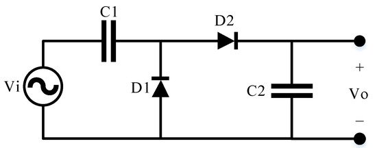
Figure 1.
Greinacher voltage doubler.
Being a simple structure, this was one of the first topologies capable of stepping up the voltage across a load powered by an AC source using only passive semiconductors and capacitors. This circuit or cell can be connected in a modular way in series or parallel with phase opposition, thus allowing the achievement of high voltages [68][69][68,69].
2.2. SC Voltage Doubler
Although the voltage step-up circuit shown in Figure 1 may be useful in some applications, its use is only feasible when an AC voltage source is available. However, many electronic circuits are powered by DC sources. The SC voltage doubler (SCVD) circuit shown in Figure 2 is a suitable alternative in this case [70][71][70,71].
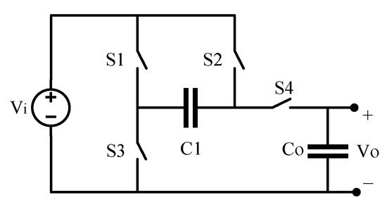
Figure 2.
SCVD.
This structure employs active switches to control the charge and discharge of the capacitors. The circuit operates in the same way as the voltage multiplier, i.e., there are two stages. In the first one, the charge of capacitor C1 occurs. In the second one, capacitor C1 is connected in series with the source and the load. It is possible to employ the connection of several cells in series to obtain a given gain 2n
, where n is the number of associated stages. Thus, it is possible to obtain high voltage gains, which allow supplying loads with high output voltages.
2.3. Cockcroft Walton Voltage Multiplier or Ladder Structure (1932)
To supply a particle accelerator with a voltage of 1 MV, Cockcroft and Walton used a circuit powered by an AC source, substantially increasing the output voltage [72]. This circuit became known as Cockcroft and Walton voltage multiplier (CWVM), or simply voltage multiplier, which is exemplified in Figure 3 in terms of several stages. This is one of the best-known structures in electronics to obtain high gains owing to the simplicity of the circuit, low cost, and simple implementation. Considering the components as ideal, the output voltage Vo can be obtained by n⋅Vi, where n is the number of associated cells and Vi is the input voltage.
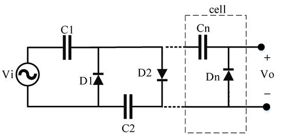
Figure 3.
CWVM.
Recent works point to the possibility of using this structure in several modern applications involving high-gain DC-DC converters associated with photovoltaic modules [73][74][73,74] and even high power factor rectifiers [75][76][77][75,76,77].
In the CWVM, the source provides some charge Q to capacitor C1 and, in each half cycle of the AC input voltage, the charge Q is transferred from capacitor to capacitor (C2, C3, …), until it reaches the last element Cn. This process involves shifting the charge through each diode similarly to a ladder, which justifies the name given to the circuit.
An inherent problem with this topology is that its output impedance increases by an n3 factor as the number of stages increases. This characteristic limits the output current to low values, as in the case of high currents; the output voltage will decrease rapidly owing to losses [78].
2.4. Series-Parallel Converter (1971)
A proposed alternative to overcome the main limitations of the CWVM in terms of voltage regulation is the series-parallel converter (SPC) shown in Figure 4 [79]. This converter is very versatile since each cell can be associated in series or parallel, and the output voltage can be modified at any time.
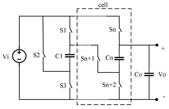
Figure 4.
SPC.
As the name suggests, the energy transfer from the input to the output occurs when connecting some of the capacitors in parallel with the source during the charge stage. In a second moment, the capacitors are associated in series and supply the load. This arrangement has some remarkable advantages because it does not present the same problems as the CWVM, especially concerning the high output impedance. However, there are other drawbacks, such as the simultaneous charging of many capacitors, which can demand a high current from the source in a short time. Also, if many capacitors are in charging process, the voltage ripple at the output may be high, directly impacting the converter efficiency. Depending on the length of the connection tracks on the printed circuit boards (PCBs), the arrangement of the elements, and the number of capacitors, there may still be problems due to parasitic capacitances, drastically reducing the efficiency of the circuit in the event of high voltage gains [80].
2.5. Series-Parallel Multiphase Converter (1973)
Another alternative to overcome the problems presented by the CWVM and the SPC is the series-parallel multiphase converter (SPMC) [81], which is shown in Figure 5. In this way, it is possible to mitigate the transients of the input current and the effect of parasitic capacitances. While part of the capacitors is connected to the source during the charge cycle, the other components that are fully charged are connected to the load. Meanwhile, part of the other series-connected capacitors remains in an intermediate charge state. Therefore, there are at least two or three phase-shifted signals controlling the connection of the capacitors with the source and the load.
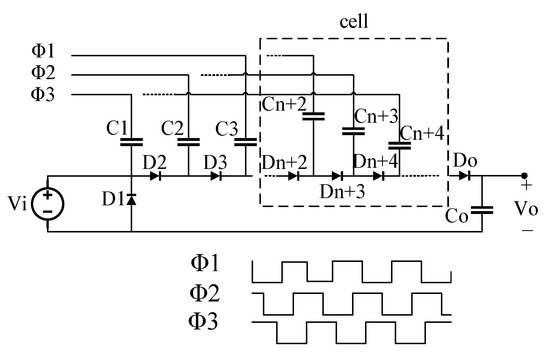
Figure 5.
SPMC.
2.6. Dickson Converter (1976)
Dickson implemented the first integrated multiphase voltage multiplier in which the circuit reached an output voltage of 40 V from a 15 V source [82]. Besides the innovation inherent in the introduction of the topology itself, it should be noted that this was the first structure built experimentally in a totally encapsulated form. Figure 6 shows the Dickson converter.
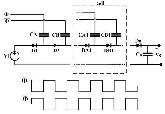
Figure 6.
Dickson converter.
In the literature, there are several publications dedicated to the study of this topology aiming at improving aspects such as efficiency, dynamic response, and regulation [83][84][85][83,84,85]. A limitation of this structure lies in the fact that it does not present good performance in high-power applications owing to the difficulty of obtaining adequate regulation and the low efficiency when it is desired to obtain high voltage gains.
2.7. Fibonacci Converter (1991)
When the first SC converters were designed, the power levels were initially limited to milliwatts or a few units of watts. A natural next step would be to reduce the number of components of these structures, aiming at increasing the gain, power levels, and efficiency. In this sense, the Fibonacci converter (FC) was proposed as a multiphase topology in which the capacitors are associated in series and parallel. In this case, the cells are combined with the source and with each other to achieve the desirable voltage gain [86]. The FC is presented in Figure 7 and receives this name because of its gain characteristic, since each cell/stage coupled to the converter leads to an increase in the output voltage following a proportion defined by the Fibonacci sequence (2, 3, 5, 8, 13, …).
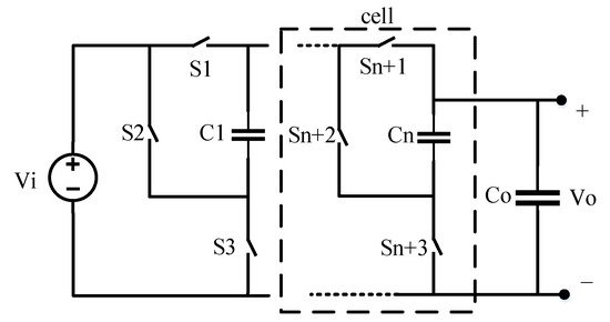
Figure 7.
FC.
The FC is very similar to the SPC, differing mainly in the way the capacitors are connected. At this point, it should be noted that among the topologies presented so far that use the combination of capacitors in series and parallel, the highest gain by the association of stages is obtained with the FC [15][87][15,87].
2.8. Ladder Converter (1992)
The CWVM can produce high voltages from a low-voltage source, but there are limitations to this structure, such as the high output impedance that prevents high gains from being achieved. In general, it can be stated that as the gain increases, the output impedance also does by a cubic factor [79], which can compromise the output voltage regulation for loads requiring high currents.
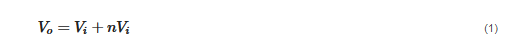
The basic ladder cells are shown in
Figure 8, which are derived from a study regarding the proposal of a three-level neutral point clamped (NPC) inverter topology [88][89]. The inverter described in [88][89] works with three voltage levels:
, which are derived from a study regarding the proposal of a three-level neutral point clamped (NPC) inverter topology [88,89]. The inverter described in [88,89] works with three voltage levels:
Vi
,
Vi
/2, and 0 V, and it is called capacitor-clamped multilevel inverter or flying capacitor multilevel inverter (FCMLI). This is a circuit similar to the NPC inverter, but the diodes are replaced by capacitors.
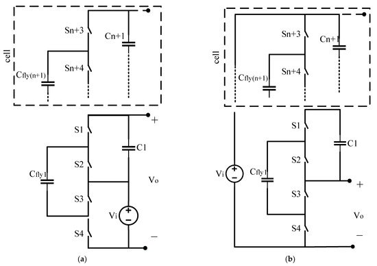
Figure 8.
(
a
) Boost and (
b
) buck ladder cells.
These cells can be arranged in the form of boost and buck configurations as shown in
a,b, respectively. A converter based on this topology can consist of one or more cells according to the desired conversion ratio. When the converter works in voltage step-up mode, the source is associated in series with
n
capacitors charged with a voltage
Vi
. The flying capacitor at a given moment is connected in parallel with the source to be charged. Still, later it is connected in parallel with the other capacitor to charge it with
Vi
. In this way, the voltage source in series with
n
charged capacitors can produce an output voltage
Vo
according to Equation (1).
when used as a step-down topology, the converter operates similarly to a capacitive voltage divider formed by
n
capacitors in series, in which the load is connected in parallel with one of the capacitors. In this circuit, there are also one or more flying capacitors
Cfly
, which at a given moment are connected in parallel with the source and later on associated in parallel with the elements that form the capacitive divider. This arrangement produces an output voltage that varies according to the number of capacitors used in the converter as defined by Equation (2):

where
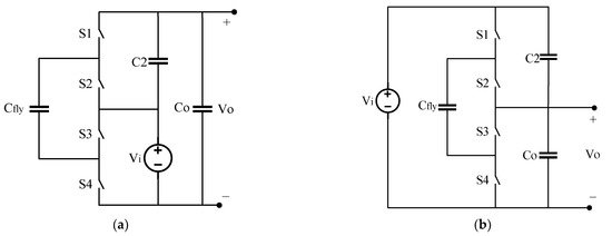
ncap
is the number of series capacitors in the circuit. a shows a boost-type ladder converter with a gain equal to two and b presents a buck converter with a gain equal to 0.5. This topology is also efficient in AC-AC conversion, with good regulation and high power factor, and it is a feasible option to replace ferromagnetic core transformers [90].
Figure 9.
(
a
) Boost and (
b
) buck ladder converters.