Your browser does not fully support modern features. Please upgrade for a smoother experience.
Please note this is a comparison between Version 1 by Giorgio Speranza and Version 2 by Lily Guo.
Carbon is a unique element of the periodic table possessing the extraordinary capability to organize its four valence electrons in different hybridization states, namely sp, sp2, sp3 leading to both strong covalent and weak π-π bonds
- carbon nanostructures
1. Introduction
Novel technological solutions are needed to face emerging global challenges such as environmental pollution, massive energy production, need of additional agricultural and food production. To increase the productivity while reducing the generation of pollutants, new advanced systems are needed to improve and automate operations which autonomously can monitor infrastructures, the environment, and the processes efficiencies [1][2][3][4][5][6][7][8][1,2,3,4,5,6,7,8]. In this respect, the potentialities enabled by sensing technologies are considerable.
The global gas sensor market size was estimated at USD 2.33 billion in 2020 and is expected to reach USD 2.50 billion in 2021. There is growing request of sensing power to monitor the environment, indoor areas, the health conditions, the industrial processes, the components in operando conditions (see applications in automotive), and sparse controls in smart cities. In this respect, the electrochemical segment dominated the market in 2020 and accounted for a share of more than 21.0% of the global revenue [9].
Nowadays there is broad class of sensors for checking gas molecules, heavy metals, humidity, recognize biomolecules, toxic substances, pH, pressure, and many others [10]. However, most of them display a non-ideal limit of detection (LOD), scarce sensitivity and/or selectivity, have slow responses, need pretreatment and are expensive. In this panorama nanomaterials can play a crucial role because they offer a solution to the limitations of conventional systems providing important advances in the material properties [10].
A revolution in material science occurred with the recognition that reduction in the nanorange of at least one of the system dimensions introduces novel unusual properties. In this respect, nanomaterials open the perspective to improve parameters such as the sensibility and the reliability, make the response and recovery times shorter, open the possibility to perform in situ analysis, and their cost is low. All these properties are required for producing sensor devices.
Nanomaterials are attractive for a number of different applications, including energy production, biomedical applications, environmental protection, information technology, food, agriculture and many others. Then, significant efforts have been recently devoted for both the mass production of structurally homogeneous nanomaterials with well controlled surfaces and interfaces and their assembly into device architectures. In this scenario, the carbon-based nanomaterials have become one of the dominating materials in several sensor applications. A literature survey reveals that more than 2200 publications are related to nanomaterial and sensing and roughly about 50% of them regard carbon nanomaterials [11].
Among the various chemical elements, carbon plays a very special role. It provides the basis for the life in nature, it displays different orbital hybridization leading to the ability to generate different chemical bonds with different orientations. For this reason, carbon possesses different allotropic forms (graphite and diamond) and has the capability to generate a list of nanostructures namely graphene single sheets, mono and multiwalled carbon nanotubes, carbon fibers, fullerenes, onions, and nanodiamonds. In addition, carbon is able to bind to nearly all chemical elements generating an unlimited variety of molecules and compounds [12] possessing a number of different chemical and physical properties. Typically the size of carbon nanomaterials ranges from 1 to 100 nm and leads to significant changes with respect to the bulk counterparts namely the increased surface to volume ratio, the nanostructure shapes, the different chemical reactivity, the different optical properties… [13].
As a consequence, carbon nanomaterials are widely utilized in many sectors. They are used in environmental applications for water treatment [14][15][14,15], and other separation processes [16][17][16,17], for environment remediation [18][19][20][18,19,20]; in electronics where they have shown remarkable utility for the excellent electrical [21][22][21,22] and optical properties [23][24][25][23,24,25]. This, combined with the molecular sized diameter and microscopic structure enable the development of novel electronic devices [26]. The high mechanical strength, electrical and thermal conductivity [27][28][29][27,28,29] make them ideal as reinforcing elements [30][31][32][30,31,32], as protective materials [33][34][35][33,34,35] and to make conductive polymers [36][37][36,37]. Carbon nanomaterials find application also in the biomedical field for sensing applications and in controlled pharmaceuticals and drugs delivery [38][39][40][41][42][38,39,40,41,42].
As mentioned before, carbon (C) atoms are able to organize themselves in different structures as depicted in Figure 1. When C atoms are arranged in a honeycomb lattice, they form the graphite crystal, a stack of two-dimensional single sheets. The single graphite layer constitutes the graphene [43] atomic crystal. Graphene nanostructures (GNs) were firstly isolated by the Nobel-prizes Geim and Novoselov in 2010. Another carbon-based structure is carbon nanotube (CNT). Discovered by Iijima in 1991, it may be regarded as a single graphene layer rolled along an axis aligned along the graphene crystalline directions [44]. As CNTs also carbon fibers (CFs) are unidimensional system. However, CFs are disordered, tangled structures possessing a two-dimensional long-range order of C atoms organized in planar hexagonal networks while in the direction orthogonal to these planes, CFs display only a short range order due to parallel plane stacking [45].
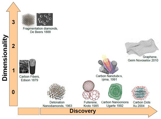
Figure 1.
Carbon nanostructures ordered following dimensionality and discovery time.
If in unidimensional carbon structures we reduce their length to the nanometer size we will obtain nanocages. Fullerenes discovered by Kroto and Smalley in 1985 is a perfectly spherical nanocage formed by a number of pentagonal and hexagonal rings [46]. Carbon nano-onions (CNOs) are cages with spherical or polyhedral shape formed by several fullerene-like overlapped carbon shells which are defective and disordered to a certain degree [47]. They were discovered in 1992 by Ugarte during electron beam irradiation of an amorphous carbon sample using a TEM microscope [48]. Another unidimensional carbon nanostructure (CNS) is represented by the carbon dots (CDs). CDs are nanoparticulate where graphitic and amorphous carbon phases coexist. Typically, the average dimension of carbon dots is about 5 nm. Quantum confinement effects induce excellent optical properties as highly tunable photoluminescence (PL), high photostability easy functionalization of their surface and biocompatibility [49] make them good competitor of quantum dots based on toxic chemical elements such as cadmium. Another CNS with excellent degree of biocompatibility is the nanodiamond. Nanodiamonds (NDs) were discovered in the sixties [50]. Depending on the synthesis process, NDs dimensions are in the 5–100 nm range. In NDs, C atoms are sp3 hybridized orbitals [51] leading to the formation of the hexagonal or cubic diamond lattices. NDs possess distinctive electronic and optical properties deriving from dopants (N, Si, Ge…) present in the structure as defects [52].
2. Properties of Carbon Nanostructures
Carbon is a unique element of the periodic table possessing the extraordinary capability to organize its four valence electrons in different hybridization states, namely sp, sp2, sp3 leading to both strong covalent and weak π-π bonds. The different hybridizations enable C-atoms to assume different allotropic forms with diamond and graphite as main prototypes and to form a wide range of structures, from small molecules to long chains [53]. The different organization of C-atoms in the crystalline lattice of graphite or diamond is also accompanied by rather different physical properties. Graphite is a stack of weakly bonded single layers where carbon atoms are organized in a honeycomb structure. Because the weak van der Waals interaction between layers, the π electrons are quasi-free thus leading to the semimetallic character of graphite [54]. The valence and conduction bands are overlapped in a point thus leading to a zero optical gap. As a consequence, the graphite has a dark aspect with high absorption coefficient. Different is the case of diamond where the sp3 hybridization generates four strong covalent bonds oriented along the axis of a tetrahedron and to a face centered Bravais lattice. In this case mobility of the electrons is absent and diamond is a highly insulating material characterized by an optical gap as high as 5.5 eV. The high optical gap makes pure diamond one of the most broadly transmitting of all materials [55]. It is transparent over a wide optical range extended well out from the visible regions (observe that absorption lines are present due to impurities mainly N, B, H, Ni…). Its transmission spectrum shows a flat featureless window for wavelengths longer than ~225 nm and moderate absorption in the range 2.6 to 6.2 μ m due to multiphonon processes [55].
Apart from these two representative forms, carbon can also organize in amorphous structures which do not display any crystalline structure. However, some short-range order can be observed in amorphous carbon (aC) phases. In aC both graphitic sp2 and tetrahedral sp3 hybrids coexist. The prevalence of one or the other of these hybrids imparts properties mirroring those of graphite or diamond. In the first case the amorphous carbon has poor mechanical properties, high extinction coefficient. Differently, in diamond-like-carbons and in highly tetrahedral amorphous carbon are very hard and the optical gap can be increased till to 4.5 eV with correspondent high transparency. Presence of hydrogen can also modulate the aC properties leading to both hard and polymer-like structures which can be interesting as biomaterials. Amorphous phases can be present in CNS or amorphous carbon nanoparticles can be produced [56][57][58][59][56,57,58,59] for their optical [60], electrical [61], mechanical properties [62].
As in the macroscopic allotropes, also the properties of a given CNS depend on the type of hybridization assumed by carbon atoms in the nanostructure. However, due to the quantum confinement imposed by the nanometric dimension or on structural arrangements as in fullerenes some differences appear. Considering the applicative point of view, the transduction of a given physical entity (generally an electrical signal) is made by the integration of a CNS into a microsystem which is used in the development of electronic, photonic, and optoelectronic devices. The selection of a given nanostructure depends on the signal to transduce and on the physicochemical properties of the CNS. In the following we will consider the properties of the single carbon nanoallotropes and the relative applications which are summarized in Figure 2.
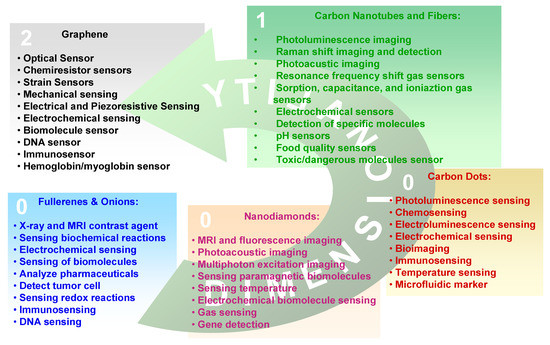
Figure 2.
Carbon nanoallotropes and the relative sensing applications.