Perovskite solar cells (PSCs) have attracted great research interest in the scientific community due to their extraordinary optoelectronic properties and the fact that their power conversion efficiency (PCE) has increased rapidly in recent years, surpassing other 3rd generation photovoltaic (PV) technologies. Graphitic carbon nitride (g-C3N4) presents exceptional optical and electronic properties and its use was recently expanded in the field of PSCs. The addition of g-C3N4 in the perovskite absorber and/or the electron transport layer (ETL) resulted in PCEs exceeding 22%, mainly due to defects passivation, improved conductivity and crystallinity as well as low charge carriers’ recombination rate within the device. Significant performance increase, including stability enhancement, was also achieved when g-C3N4 was applied at the PSC interfaces and the observed improvement was attributed to its wetting (hydrophobic/hydrophilic) nature and the fine tuning of the corresponding interface energetics.
1. Background
In today’s industrial societies, energy needs are constantly growing, and become harder to fulfill. Energy production comes mostly from the combustion of fossil fuels, and has a major impact on climate change [1]. Solar energy is one of the most significant sources of renewable energy and researchers have extensively endeavored to use it in order to address these concerns [2]. Solar energy is characterized by abundance and ease of use, and have already showed a great potential to be a prime source of energy in the future [3]. In recent years, it has attracted scientific and technological interest in the direction of its utilization and efficient conversion into other useful forms of energy. Photovoltaic (PV) devices are the basic technology for this process. The technologically mature PV panels based on silicon (Si) already occupy a large share in global energy production/consumption. Nevertheless, the implementation of the Si-based technology is limited by high fabrication cost of the corresponding modules and panels [4]. Additionally, the commercialization of the 2nd generation solar cells (Si, CdTe, CIGS) is, mainly, hindered due to module stability issues [5].
Recent developments in photovoltaic research have shown that silicon cells, which still dominate the market, can be replaced by new cells based on more efficient and cheaper materials, such as perovskites. Lately, the scientific community has focused on this type of 3rd generation cells, as their near-ideal optoelectronic properties [6], including the tunable band gap, high carrier mobility [7], long carrier lifetime [8], and the solution-processed and low-cost fabrication methods [9], make them very promising as light absorbers. The power conversion efficiency (PCE) of perovskite solar cells (PSCs) has increased rapidly in recent years, exceeding 25% within only a few years of development [10][11][12][13][14][15][16] (
Recent developments in photovoltaic research have shown that silicon cells, which still dominate the market, can be replaced by new cells based on more efficient and cheaper materials, such as perovskites. Lately, the scientific community has focused on this type of 3rd generation cells, as their near-ideal optoelectronic properties [6], including the tunable band gap, high carrier mobility [7], long carrier lifetime [8], and the solution-processed and low-cost fabrication methods [9], make them very promising as light absorbers. The power conversion efficiency (PCE) of perovskite solar cells (PSCs) has increased rapidly in recent years, exceeding 25% within only a few years of development [10,11,12,13,14,15,16] ( a), surpassing other 3rd generation PV technologies. However, several issues including further efficiency increase and performance stabilization have not been effectively addressed yet. In fact, grain size and crystallinity of the perovskite films, conductivity of the functional layers, charge recombination, surface and intrinsic defects, hysteresis phenomena, and chemical/thermal stability under continuous sun illumination in atmospheric environment, are main issues that require to be effectively addressed. Research interventions aiming for further development of these photovoltaic devices have in common the integration of innovative nanostructured materials in order to increase their PCE, improve their long-term stability and decrease their fabrication cost. Among this purpose, several strategies, such as materials and interface engineering [17][18][19][20][21][22][23][24][25][26], have been reported.
a), surpassing other 3rd generation PV technologies. However, several issues including further efficiency increase and performance stabilization have not been effectively addressed yet. In fact, grain size and crystallinity of the perovskite films, conductivity of the functional layers, charge recombination, surface and intrinsic defects, hysteresis phenomena, and chemical/thermal stability under continuous sun illumination in atmospheric environment, are main issues that require to be effectively addressed. Research interventions aiming for further development of these photovoltaic devices have in common the integration of innovative nanostructured materials in order to increase their PCE, improve their long-term stability and decrease their fabrication cost. Among this purpose, several strategies, such as materials and interface engineering [17,18,19,20,21,22,23,24,25,26], have been reported.
Figure 1.
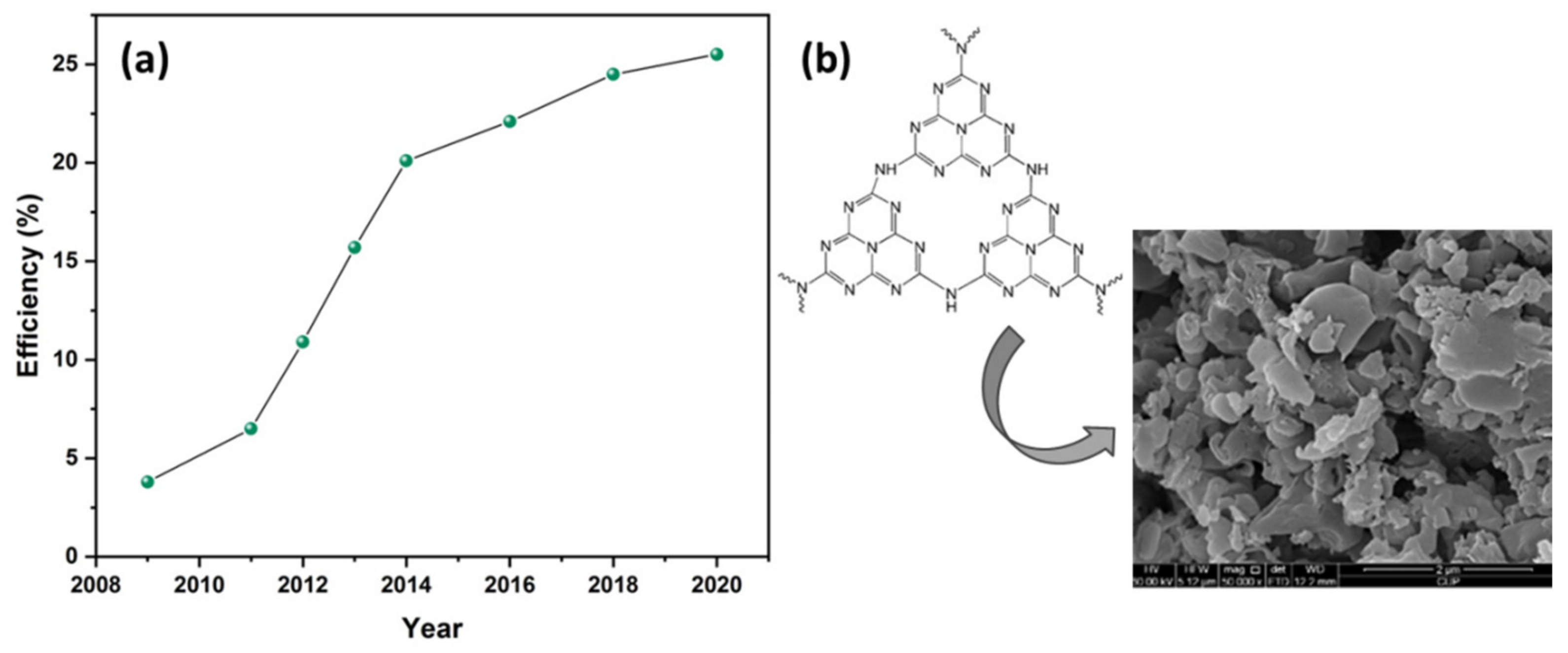
(
a
) Perovskite solar cells’ (PSCs’) certified efficiency evolution 2009–2020 and (
b
) the structure and morphology (SEM image) of graphitic carbon nitride (g-C
3
N
4
). Reproduced with permission from [27], Copyright 2014, Elsevier.
2. Working Principles and Challenges of PSCs
Perovskite materials have been studied either as sunlight absorbers [28] or as hole transport materials [29] in photovoltaic cells, due to their special properties, such as the high absorption coefficient [7][30], the high mobility load carriers [31], long charge carrier diffusion length [32], wide absorption spectrum, and configurable energy gap. Perovskite materials exhibit the stoichiometry ABX
Perovskite materials have been studied either as sunlight absorbers [57] or as hole transport materials [58] in photovoltaic cells, due to their special properties, such as the high absorption coefficient [7,59], the high mobility load carriers [60], long charge carrier diffusion length [61], wide absorption spectrum, and configurable energy gap. Perovskite materials exhibit the stoichiometry ABX 3 [33]. For photovoltaic applications, A is usually an organic cation, such as methylammonium (CH
[62]. For photovoltaic applications, A is usually an organic cation, such as methylammonium (CH 3
NH
3+) [34] and formamidinium (HC(NH
) [63] and formamidinium (HC(NH 2
)
2+) [35], or an inorganic, such as Cs
) [64], or an inorganic, such as Cs +
, or a combination of them, B is a metal cation (usually Pb
2+
or Sn
2+
), while the X position represents a non-metallic anion such as the halogens Cl
−
, Br
−
, I
− and the combination of these [36].
and the combination of these [65]. a [37] illustrates the crystal structure of ABX
a [66] illustrates the crystal structure of ABX 3
.
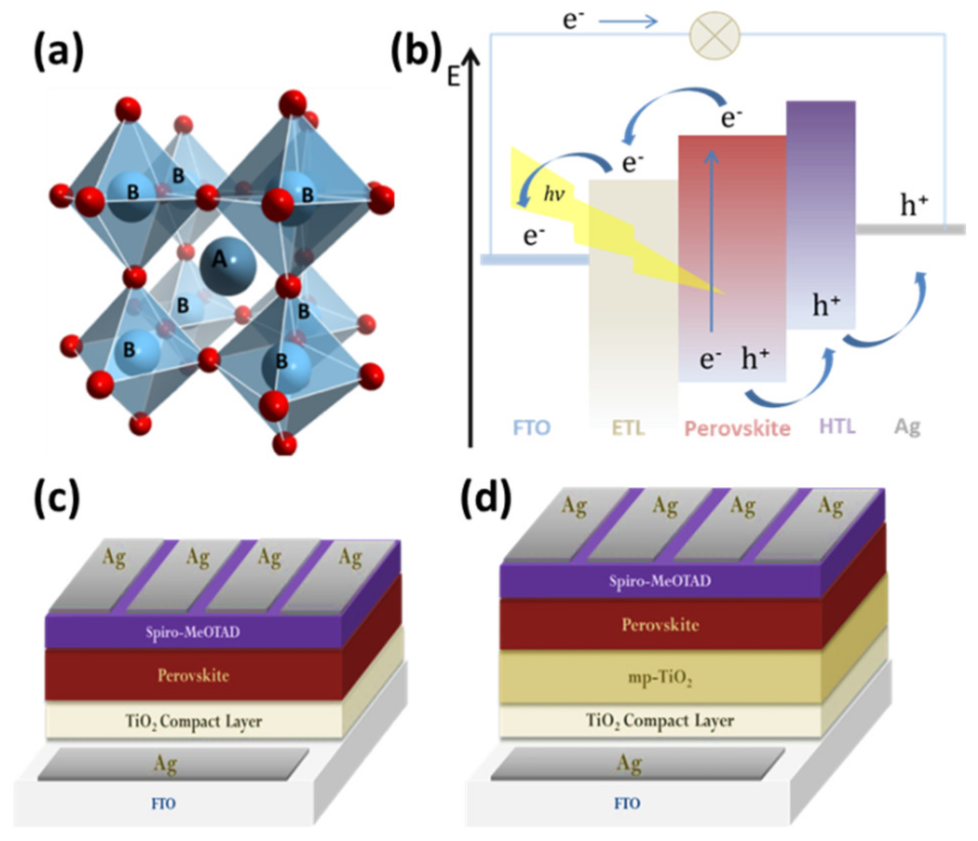
Figure 2.
(a
) Illustration of the general perovskite crystal structure, (b
) the working mechanism of a PSC, and (c
,d) the two typical device architectures; planar and mesoporous, respectively. Reproduced with permission from [38], Copyright 2019, Elsevier.
) the two typical device architectures; planar and mesoporous, respectively. Reproduced with permission from [73], Copyright 2019, Elsevier.
The PSC’s working mechanism includes the absorption of photons [39] from the absorber/perovskite and the transfer and extraction of charge carriers to the respective electrodes. Specifically, photons’ absorption is followed by the presence of excited electrons in the conduction band and holes in the valence band of the perovskite. The electrons are injected into ETL and migrate to the anode. Subsequently, the electron passes through the external circuit to the cathode. At the same time, the holes are transferred through the hole transport layer (HTL) and migrate to the cathode, where electrons and holes recombine (
The PSC’s working mechanism includes the absorption of photons [67] from the absorber/perovskite and the transfer and extraction of charge carriers to the respective electrodes. Specifically, photons’ absorption is followed by the presence of excited electrons in the conduction band and holes in the valence band of the perovskite. The electrons are injected into ETL and migrate to the anode. Subsequently, the electron passes through the external circuit to the cathode. At the same time, the holes are transferred through the hole transport layer (HTL) and migrate to the cathode, where electrons and holes recombine ( b). Charge carrier extraction occurs at the perovskite/ETL and perovskite/HTL interfaces and, then, at the ETL/anode and HTL/cathode interfaces. Thus, the overall photovoltaic performance of PSCs is greatly affected by the properties of these interfaces. Two types of PSC device architectures exist, depending on the ETL and HTL ordering. The case of the ETL, which is an n-type semiconductor, being placed before the perovskite and the HTL, which is a p-type semiconductor, after perovskite attributes to the n–i–p structure, while the opposite attributes to the p–i–n structure [40][41][42]. In the case of the n-i-p type PSCs, planar [43][44] or mesoporous [14][38] configurations can be distinguished, depending on the morphology of the ETL material (
b). Charge carrier extraction occurs at the perovskite/ETL and perovskite/HTL interfaces and, then, at the ETL/anode and HTL/cathode interfaces. Thus, the overall photovoltaic performance of PSCs is greatly affected by the properties of these interfaces. Two types of PSC device architectures exist, depending on the ETL and HTL ordering. The case of the ETL, which is an n-type semiconductor, being placed before the perovskite and the HTL, which is a p-type semiconductor, after perovskite attributes to the n–i–p structure, while the opposite attributes to the p–i–n structure [68,69,70]. In the case of the n-i-p type PSCs, planar [71,72] or mesoporous [14,73] configurations can be distinguished, depending on the morphology of the ETL material ( c,d). Nevertheless, in addition to the perovskite absorber deposited on the ETL, a complete PSC device also comprises the electron collection substrate, usually a conducting oxide glass such as fluorine-doped tin oxide (FTO) or indium tin oxide (ITO) and the hole transporting layer (HTL) in contact with a metallic (Au, Ag) or carbon upper electrode [45][46].
c,d). Nevertheless, in addition to the perovskite absorber deposited on the ETL, a complete PSC device also comprises the electron collection substrate, usually a conducting oxide glass such as fluorine-doped tin oxide (FTO) or indium tin oxide (ITO) and the hole transporting layer (HTL) in contact with a metallic (Au, Ag) or carbon upper electrode [74,75].
Nowadays, PSCs have already reached a high efficiency in a very short period of research activity; however, there are other factors that also need to be addressed. First of all, during the charge carriers’ transfer and extraction through the successive layers, excess of carriers are not collected and recombine (radiatively or nonradiatively) at the interfaces [47][48]. Other challenges in the field of PSCs are the thermal and chemical stability [49] of the constituent materials and the overall device, hysteresis phenomenon [50][51], intrinsic and surface defects [52][53], enhanced charge carriers’ mobility and lead’s toxicity. Towards the mitigation of these problems a number of material and interface engineering approaches have been proposed including the integration of reduced graphene oxide as additive in the ETL, the perovskite and the HTL, the passivation of the ETL’s surface with metallated porphyrins and organic dyes, the modification of the titania ETL with transition metals, such copper and niobium, the passivation of perovskite layer’s surface with formamidinium iodide solution in isopropyl alcohol, and the addition of 4-tert-butylpyridine (tBP) in perovskite precursor as surface modification agent [17][18][19][20][21][22][23][24][25][26]. The incorporation of graphitic carbon nitride has been proved to be an efficient method for controlling crystal growth, passivating defects and reducing charge carriers’ recombination rate, and, thus, confronting many of the above-mentioned challenges.
Nowadays, PSCs have already reached a high efficiency in a very short period of research activity; however, there are other factors that also need to be addressed. First of all, during the charge carriers’ transfer and extraction through the successive layers, excess of carriers are not collected and recombine (radiatively or nonradiatively) at the interfaces [76,77]. Other challenges in the field of PSCs are the thermal and chemical stability [78] of the constituent materials and the overall device, hysteresis phenomenon [79,80], intrinsic and surface defects [81,82], enhanced charge carriers’ mobility and lead’s toxicity. Towards the mitigation of these problems a number of material and interface engineering approaches have been proposed including the integration of reduced graphene oxide as additive in the ETL, the perovskite and the HTL, the passivation of the ETL’s surface with metallated porphyrins and organic dyes, the modification of the titania ETL with transition metals, such copper and niobium, the passivation of perovskite layer’s surface with formamidinium iodide solution in isopropyl alcohol, and the addition of 4-tert-butylpyridine (tBP) in perovskite precursor as surface modification agent [17,18,19,20,21,22,23,24,25,26]. The incorporation of graphitic carbon nitride has been proved to be an efficient method for controlling crystal growth, passivating defects and reducing charge carriers’ recombination rate, and, thus, confronting many of the above-mentioned challenges.
3. Properties of g-C3N4
Intense theoretical and experimental interest has been focused on materials with tunable properties. Among these, carbon nitrides have attracted great attention due to their relative stability, structure and physicochemical properties [54]. In particular graphitic carbon nitride (g-C
Intense theoretical and experimental interest has been focused on materials with tunable properties. Among these, carbon nitrides have attracted great attention due to their relative stability, structure and physicochemical properties [83]. In particular graphitic carbon nitride (g-C 3
N
4
) as a pyrolysis product of nitrogen-rich precursors, such as dicyandiamide, melamine, thiourea, and urea has attracted significant interest among the research community.
Graphitic carbon nitride presents very interesting structural and oproelectronic properties. Following polymerization, the existing basic core triazine C
3
N
3
(melam) and tri-s-triazine C
6
N
7 (melem) planar units create a layered structure similar to graphite. The typical XRD peaks are placed at 2θ ~27° and 2θ ~13° [55], from which the first is related to interlayer stacking of the (002) melem planes and the second is attributed to the (100) planes corresponding to inplane ordering of the nitrogen-linked heptazine units. As in the case of graphite, the C
(melem) planar units create a layered structure similar to graphite. The typical XRD peaks are placed at 2θ ~27° and 2θ ~13° [84], from which the first is related to interlayer stacking of the (002) melem planes and the second is attributed to the (100) planes corresponding to inplane ordering of the nitrogen-linked heptazine units. As in the case of graphite, the C 3
N
3
and C
6
N
7
cores comprise six-membered rings with sp
2 C-N hybridization presenting intrinsic structural vacancies surrounded by nitrogen atoms [56]. Depending on the precursor and the conditions of the pyrolysis used, the
C-N hybridization presenting intrinsic structural vacancies surrounded by nitrogen atoms [49]. Depending on the precursor and the conditions of the pyrolysis used, the g
-C
3
N
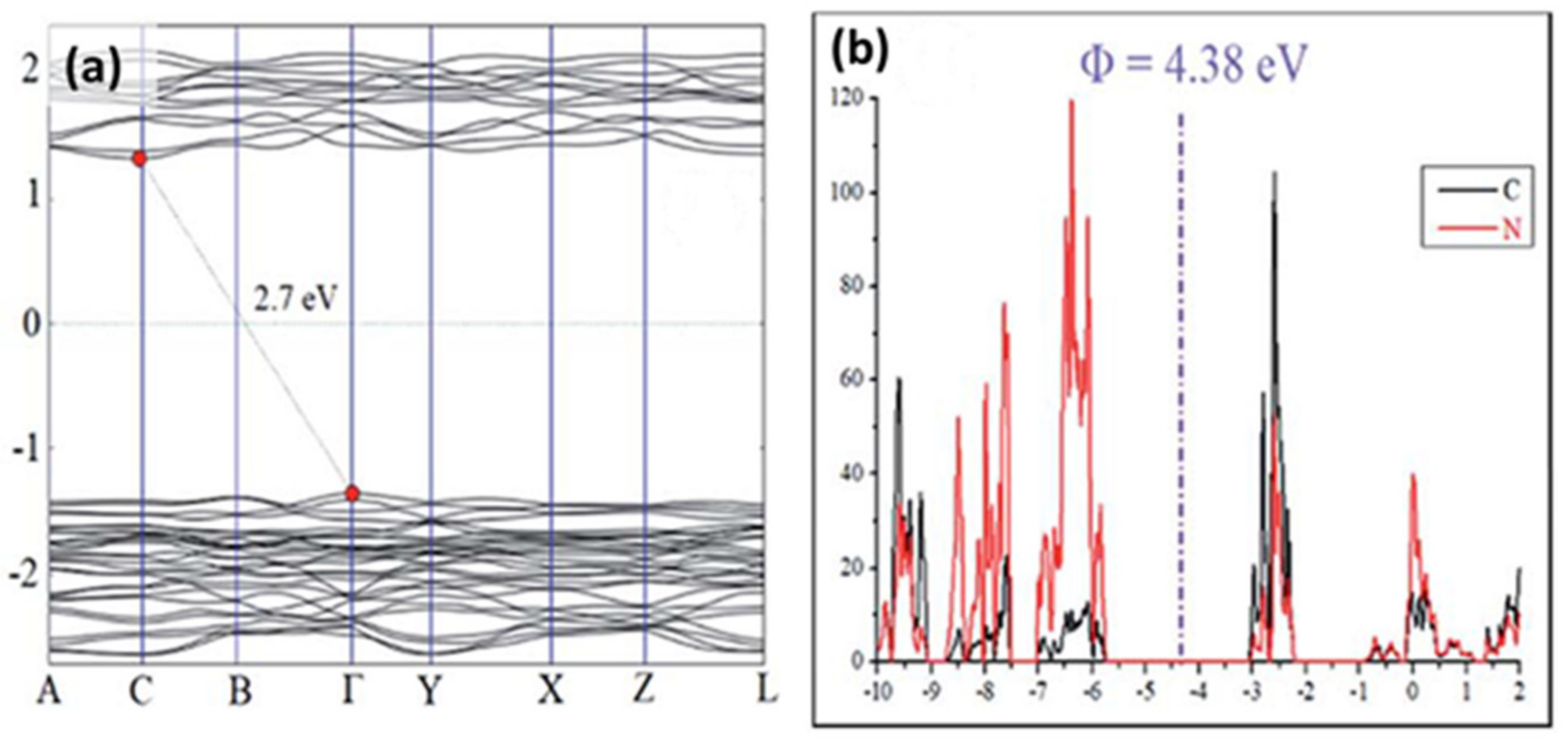
4 powders have the possibility to result in different structures from highly crystalline samples to bulk (high temperature) and tubular (low temperature) samples [57][58]. In fact, DFT calculations were performed on carbon nitride single-layer to evaluate the structural and optoelectronic properties. The obtained results are consistent with a layered structure of slightly buckled heptazine cores, where the observed distortion can be attributed to electrostatic repulsions on the triazine-rings involving the two-coordinated N atoms with lone pair electrons [59]. Density of states (DOS) calculations (
powders have the possibility to result in different structures from highly crystalline samples to bulk (high temperature) and tubular (low temperature) samples [85,86]. In fact, DFT calculations were performed on carbon nitride single-layer to evaluate the structural and optoelectronic properties. The obtained results are consistent with a layered structure of slightly buckled heptazine cores, where the observed distortion can be attributed to electrostatic repulsions on the triazine-rings involving the two-coordinated N atoms with lone pair electrons [87]. Density of states (DOS) calculations ( a) have demonstrated that g-C
3
N
4
is a semiconducting material having a moderate band gap of 2.7 eV. Moreover, the corresponding analysis of partial density of states indicates the position of the valence band and the conduction band at −5.74 and −3.07 eV (vs. vacuum), respectively (
b) [60][61].
Figure 3.
(a
) g-C3
N4
band structure from density of states (DOS) calculations and (b) analysis of partial density of states (PDOS) comprising C and N orbitals. Reproduced with permission from [61], Copyright 2018, Elsevier.
) analysis of partial density of states (PDOS) comprising C and N orbitals. Reproduced with permission from [42], Copyright 2018, Elsevier.
So far, numerous methods have been used in order to modify the surface of bulk graphitic carbon nitride for different purposes. Chemical and thermal exfoliation [62] has been used in order to increase the active surface area as well as the optical properties. It becomes apparent that the exfoliation of bulk graphitic carbon nitride into 2D structure yields in an elevated bandgap, in agreement with the observed color modification of the samples to light yellow (from dark ones). [63][64]. Doping with heteroatoms [65] leads to an enhancement of the electrical conductivity and photoactivity due to the substitution of C or N by B, S, and Fe atoms of different valence in the honeycomb lattice. Such substitution introduces supplementary states in the density of states and usually involves nitrogen and boron as doping elements as their valence number is closer, in comparison to carbon atoms [66]. Finally, the introduction of functional groups leads to improved electrochemical properties as a result of changes in conductivity resulting from delocalized π-electrons, adsorbed species and defect sites [67]. Thus, the research community has focused on graphitic carbon nitride (g-C
So far, numerous methods have been used in order to modify the surface of bulk graphitic carbon nitride for different purposes. Chemical and thermal exfoliation [88] has been used in order to increase the active surface area as well as the optical properties. It becomes apparent that the exfoliation of bulk graphitic carbon nitride into 2D structure yields in an elevated bandgap, in agreement with the observed color modification of the samples to light yellow (from dark ones). [89,90]. Doping with heteroatoms [91] leads to an enhancement of the electrical conductivity and photoactivity due to the substitution of C or N by B, S, and Fe atoms of different valence in the honeycomb lattice. Such substitution introduces supplementary states in the density of states and usually involves nitrogen and boron as doping elements as their valence number is closer, in comparison to carbon atoms [92]. Finally, the introduction of functional groups leads to improved electrochemical properties as a result of changes in conductivity resulting from delocalized π-electrons, adsorbed species and defect sites [93]. Thus, the research community has focused on graphitic carbon nitride (g-C 3
N
4) as a metal free, nontoxic and VLA (visible light activated) photocatalyst with a unique 2D structure, outstanding chemical stability and tunable physicochemical properties [68][69]. Compared to other materials reported in literature for PSCs engineering, the advantages of g-C
) as a metal free, nontoxic and VLA (visible light activated) photocatalyst with a unique 2D structure, outstanding chemical stability and tunable physicochemical properties [55,56]. Compared to other materials reported in literature for PSCs engineering, the advantages of g-C 3
N
4
can be attributed to its tunable structural and optoelectronic properties which can be optimized to the needs of the PSC technology. The carbon nitride material, characterized by easy and low-cost fabrication, also disposes high chemical and thermal stability that is required for the long-term operation of robust PSC devices. In general, the incorporation of bulk or modified g-C
3
N
4
into solar cells is desirable in order to achieve highly stable and efficient performances.
4. Incorporation of g-C3N4 in PSCs
Recent studies have shown that nitrogen-rich precursors demonstrated enhanced PCE for PSCs. It seems that the incorporation of nitrogen functionalities has resulted in effective passivation of organic–inorganic halide perovskite materials [68][69]. In 2017, Lee et al. [70] reported that the defect sites of methylammonium lead tribromide (MAPbBr
Recent studies have shown that nitrogen-rich precursors demonstrated enhanced PCE for PSCs. It seems that the incorporation of nitrogen functionalities has resulted in effective passivation of organic–inorganic halide perovskite materials [55,56]. In 2017, Lee et al. [94] reported that the defect sites of methylammonium lead tribromide (MAPbBr 3) were passivated through coordinate bonding between the nitrogen atoms and undercoordinated lead ions, by using amine-based treatment on top of the perovskite film. In another study by Hsieh et al. [68], they used urea and thiourea, previously dissolved in DMF at a concentration of 25 wt% and stirred overnight, as additives in MAPbI
) were passivated through coordinate bonding between the nitrogen atoms and undercoordinated lead ions, by using amine-based treatment on top of the perovskite film. In another study by Hsieh et al. [55], they used urea and thiourea, previously dissolved in DMF at a concentration of 25 wt% and stirred overnight, as additives in MAPbI 3−x
Cl
x
and MAPbI
3
perovskite solar cells. In both cases, the PCE was improved and the MAPbI
3
based PSC presented a PCE of 18.8% (from 14.6% in the reference cell). The authors characterized the additives containing perovskite absorbers using UV-vis spectroscopy, scanning electron microscopy and grazing incidence wide angle X-ray diffraction measurements and attributed the observed performance enhancement to reduced grain boundaries of MAPbI
3
hindering charge recombination and allowing the effective charge carriers (electrons and holes) transport. Similarly, by incorporating 4mol% of urea (a bifunctional nonvolatile Lewis base) in MAPbI
3, Lee et al. [71] obtained significantly enhanced photoluminescence lifetime accompanied by suppression of the trap-related nonradiative recombination. XRD analysis and FTIR spectroscopy were used to monitor both the perovskite growth and intramolecular interactions. In parallel, time-resolved photoluminescence (TRPL) measurements permitted the determination of charge-carrier lifetime and trap densities. Thus, the interaction of urea with the perovskite precursors in solution was confirmed. The urea additive retards growth and enhances perovskite crystallinity, and then passivates defects in the absorber by precipitating at the grain boundaries.
, Lee et al. [95] obtained significantly enhanced photoluminescence lifetime accompanied by suppression of the trap-related nonradiative recombination. XRD analysis and FTIR spectroscopy were used to monitor both the perovskite growth and intramolecular interactions. In parallel, time-resolved photoluminescence (TRPL) measurements permitted the determination of charge-carrier lifetime and trap densities. Thus, the interaction of urea with the perovskite precursors in solution was confirmed. The urea additive retards growth and enhances perovskite crystallinity, and then passivates defects in the absorber by precipitating at the grain boundaries.
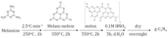
Graphitic carbon nitride is a pyrolysis product of nitrogen-rich precursors (
). Its incorporation in PSCs has attracted scientific attention only in the few last years. However, the up-to-now findings appear to be promising and of high interest for the emerging perovskite solar cells.
Figure 4.
Schematic diagram of a typical pyrolysis procedure for g-C3
N4
fabrication.
4.1. g-C
3
N
4
Modified Perovskite Absorbers
In the few past years many studies have focused on the incorporation of g-C
3
N
4 into the perovskite layer as a passivation strategy for the improvement of the crystallinity, which is a complicated process, the conductivity and, thus, the overall performance of the devices. Towards this strategy, the work from Liao et al. [72] refers to the incorporation of a small amount of g-C
into the perovskite layer as a passivation strategy for the improvement of the crystallinity, which is a complicated process, the conductivity and, thus, the overall performance of the devices. Towards this strategy, the work from Liao et al. [96] refers to the incorporation of a small amount of g-C 3
N
4
derived by standard pyrolysis of dicyandiamide, into the perovskite ink, which revealed impressive PCEs up to 21.1%. The addition of g-C
3
N
4
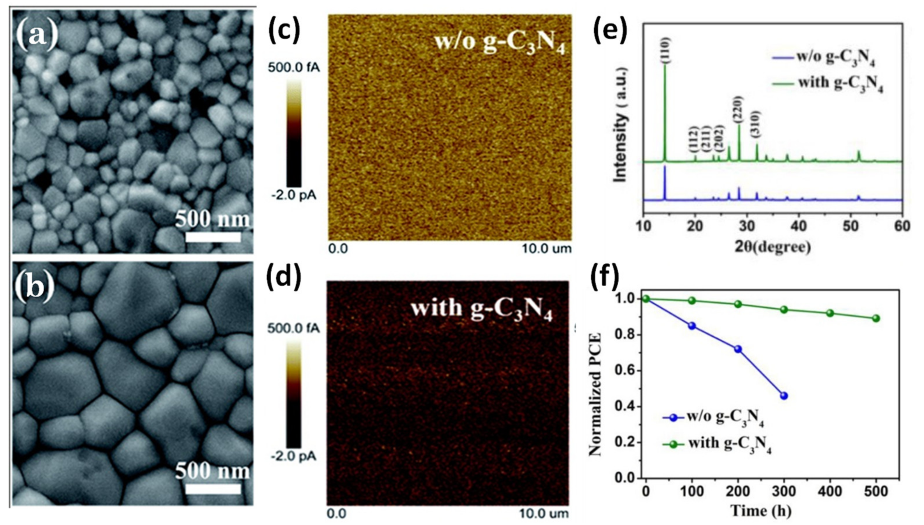
led to compact perovskite films with passivated defects, large grain sizes, improved conductivity, and high crystallinity (
a–e), as confirmed by SEM, FTIR, XPS, and c-AFM measurements, which led to devices with considerably low charge recombination rate. The g-C
3
N
4
modified PSCs are characterized by extremely low hysteresis accompanied by enhanced stability. In fact, after 500 h continuous illumination under one sun, only about 10% decline in devices PCE was observed (
f).
Figure 5.
Top-view SEM images of the perovskite films based on (a
) control MAPbI3
and (b
) 0.1 wt% g-C3
N4
modified MAPbI3
film, conductive AFM images of (c
) control MAPbI3
and (d
) 0.1 wt% g-C3
N4
modified MAPbI3
films with a scanning area of 10 × 10 μm2
, (e
) XRD patterns of control and 0.1 wt% g-C3
N4
modified MAPbI3
films, and (f
) operational stability of the encapsulated PSCs fabricated with or without g-C3
N4 under constant 1 sun illumination. Reproduced with permission from [72], Copyright 2019, The Royal Society of Chemistry.
under constant 1 sun illumination. Reproduced with permission from [96], Copyright 2019, The Royal Society of Chemistry.
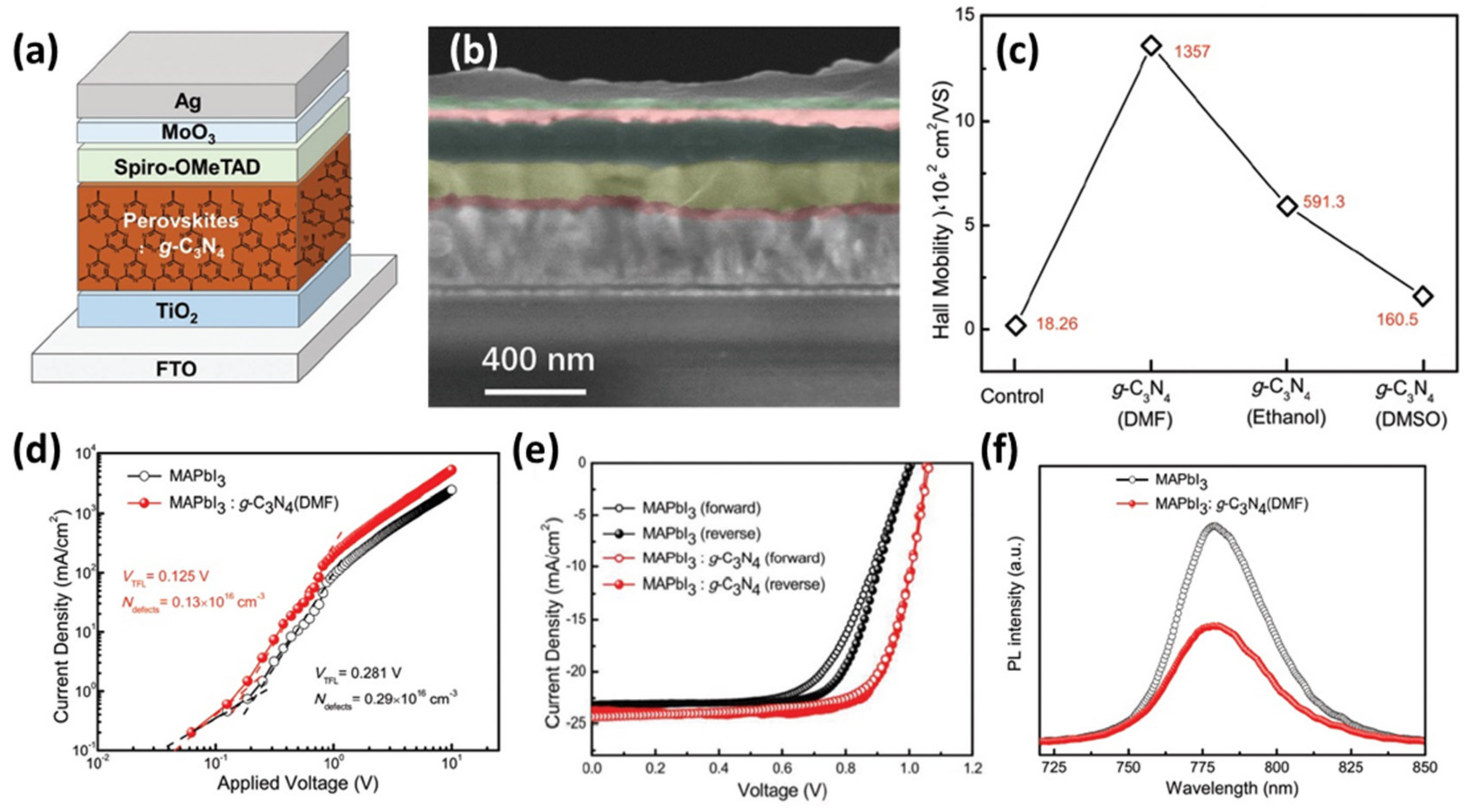
Similarly, in a previous work Jiang et al. [69] reported that the addition of 0.6 wt% pure sheets of g-C
Similarly, in a previous work Jiang et al. [56] reported that the addition of 0.6 wt% pure sheets of g-C 3
N
4
produced by standard pyrolysis of urea into MAPbI
3
layer (
a,b) increased the crystallization and grain sizes of the perovskite film, proved by SEM characterization, as well as, its carrier mobility (
c). Thus, conductive AFM measurements confirmed the improvement of the corresponding perovskite absorber/spiro HTM interface. In parallel, the defects density was reduced ((
d) which consequently reduced hysteresis (
e) and increased the PCE from 16.22% to 19.49%. In this work the authors examined thoroughly the impact of different solvents, which were used to dissolve g-C
3
N
4
, on the perovskite’s crystal growth and managed to control the crystallization and reduce the charge recombination (
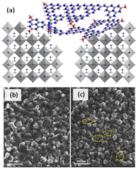
f). Among the employed solvents (DMF, DMSO, ethanol), DMF did not show to significantly affect the cell parameters. In a similar vein, Wei et al. [73] prepared ultrafine E-g-C
f). Among the employed solvents (DMF, DMSO, ethanol), DMF did not show to significantly affect the cell parameters. In a similar vein, Wei et al. [97] prepared ultrafine E-g-C 3
N
4
nanoparticles, using melamine precursor and annealing at 550 °C followed by intercalation in H
2
SO
4
and fast stripping in NH
3
aqueous solution. The obtained nanomaterials, self-located at the MAPbI
3
grain boundaries via hydrogen bonding interaction (
), worked as prohibitory of electron-hole recombination. Thus, they were successfully incorporated into PSCs improving the device performance by 35%.
Figure 6.
(a
) Architecture of MAPbI3
:g-C3
N4
based n-i-p PSC and (b
) corresponding cross-sectional SEM image, (c
) Hall mobility of MAPbI3
and MAPbI3
:g-C3
N4
in various solvents films, (d
) current density–voltage (J–V) curves of hole-dominated devices with a structure of FTO/PEDOT:PSS/MAPbI3
(with and without g-C3
N4
)/MoO3
/Ag, (e
) J–V curves of MAPbI3
and MAPbI3
:g-C3
N4
based devices by forward and reverse scan, and (f
) photoluminescence (PL) spectra of MAPbI3
and MAPbI3
:g-C3
N4
(DMF) films deposited on TiO2/FTO. Reproduced with permission from [69], Copyright 2017, Wiley-VCH GmbH.
/FTO. Reproduced with permission from [56], Copyright 2017, Wiley-VCH GmbH.
Figure 7.
(a
) Schematic illustration of the self-location process of E-g-C