Perovskite solar cells (PSCs) are the most promising substitute for silicon-based solar cells. However, their power conversion efficiency and stability must be improved. The recombination probability of the photogenerated carriers at each interface in a PSC is much greater than that of the bulk phase. The interface of a perovskite polycrystalline film is considered to be a defect-rich area, which is the main factor limiting the efficiency of a PSC.
1. Introduction
Organic–inorganic hybrid perovskite materials exhibit excellent photoelectric properties (e.g., an adjustable band gap, a long carrier life, a long carrier diffusion length, a low exciton binding energy, a high molar extinction coefficient, low cost, and an easy preparation) and are widely used in various optoelectronic devices, such as solar cells, light-emitting diodes, photodetectors, memristors, and sensors [1][2][3][4][5][6][7][8]. Among such devices, perovskite solar cells (PSCs) have been the most frequently investigated [9]. According to calculations based on the Shockley–Queisser limit theory, a light-absorbing material with a bandgap of 1.6 eV can achieve a theoretical limit efficiency of approximately 30.5% [10]. Current single-junction PSCs have achieved a certified power conversion efficiency (PCE) of 25.5% [11][12]. However, this value is still lower than the theoretical efficiency; therefore, there remains room for improving the performance of PSCs.
Organic–inorganic hybrid perovskite materials exhibit excellent photoelectric properties (e.g., an adjustable band gap, a long carrier life, a long carrier diffusion length, a low exciton binding energy, a high molar extinction coefficient, low cost, and an easy preparation) and are widely used in various optoelectronic devices, such as solar cells, light-emitting diodes, photodetectors, memristors, and sensors [1,2,3,4,5,6,7,8]. Among such devices, perovskite solar cells (PSCs) have been the most frequently investigated [9]. According to calculations based on the Shockley–Queisser limit theory, a light-absorbing material with a bandgap of 1.6 eV can achieve a theoretical limit efficiency of approximately 30.5% [10]. Current single-junction PSCs have achieved a certified power conversion efficiency (PCE) of 25.5% [11,12]. However, this value is still lower than the theoretical efficiency; therefore, there remains room for improving the performance of PSCs.
In a PSC, the most commonly used perovskite material is the organic–inorganic metal halide perovskite, CH
3
NH
3
PbX
3
(MAPbX
3
), the structure of which is shown in
. Its disadvantages include a poor stability and low open-circuit voltage. Therefore, different metal cations, organic cations, and halogens can be used to replace the corresponding elements or ions in traditional materials [13]. In addition, HC(NH 2
)
2(FA) and Cs can be used to replace MA owing to their wider absorption range; consequently, a bandgap corresponding to the entire wavelength range of visible light can be achieved, thereby resulting in a higher energy conversion rate [14][15]. Tin-based PSCs exhibit electronic structures and semiconductor properties that are similar to those of perovskites, including a high absorption coefficient, high carrier mobility, and an ideal bandgap [16][17][18]. This is ideal for the manufacture of environmentally friendly PSCs. As promising alternatives to tin, transition metals such as Fe, Cu, Mn, Ni, and Co are rich in reserves and contain diverse ion valences [19]. The addition of halogen elements Cl and Br promotes a non-uniform nucleation at different positions and improves the morphology of perovskite films, thereby facilitating carrier transport and reducing the carrier recombination [20][21][22]. Improvements in the morphology and microstructure of the film by optimizing the preparation process for control of the nucleation density and growth rate of the crystal can increase the PCE. A one- (
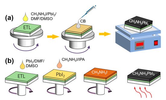
(FA) and Cs can be used to replace MA owing to their wider absorption range; consequently, a bandgap corresponding to the entire wavelength range of visible light can be achieved, thereby resulting in a higher energy conversion rate [14,15]. Tin-based PSCs exhibit electronic structures and semiconductor properties that are similar to those of perovskites, including a high absorption coefficient, high carrier mobility, and an ideal bandgap [16,17,18]. This is ideal for the manufacture of environmentally friendly PSCs. As promising alternatives to tin, transition metals such as Fe, Cu, Mn, Ni, and Co are rich in reserves and contain diverse ion valences [19]. The addition of halogen elements Cl and Br promotes a non-uniform nucleation at different positions and improves the morphology of perovskite films, thereby facilitating carrier transport and reducing the carrier recombination [20,21,22]. Improvements in the morphology and microstructure of the film by optimizing the preparation process for control of the nucleation density and growth rate of the crystal can increase the PCE. A one- ( a) or two-step (
b) method is typically used to prepare high-performance PSCs [23][24][25]. Furthermore, the dual-source vapor deposition method, two-step continuous solution-vapor assisted deposition method, and other approaches have been applied to the optimization of perovskite films for improving the PCE of PSCs [15][26][27].
b) method is typically used to prepare high-performance PSCs [23,24,25]. Furthermore, the dual-source vapor deposition method, two-step continuous solution-vapor assisted deposition method, and other approaches have been applied to the optimization of perovskite films for improving the PCE of PSCs [15,26,27].
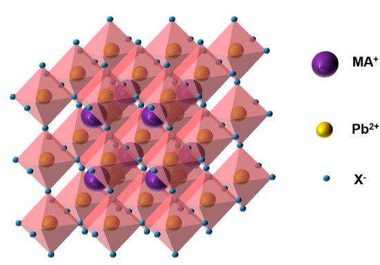
Figure 1.
Structure of MAPbX
3.
Figure 2.
(
a
) One- and (
b
) two-step methods.
In addition to the development of new materials and the optimization of the preparation process, the selection of interface materials and the generation, collection, and transport efficiency of interface charges are crucial to the performance of a PSC [2][3][4][14]. The typically investigated flat-panel sandwich-structured PSCs are disadvantageous owing to their significant interface recombination, low carrier separation efficiency, and low stability, all of which have restricted their development. Many studies have proven that the efficiency and stability of perovskite solar cells are closely associated with the nonradiative recombination loss of bulk and interface carriers [28]. Effective methods for the further development of PSCs include optimizing their structure, improving the charge separation and extraction rate at the interface, and reducing the effect of the organic material degradation on the device stability [15][29]. The interface engineering of PSCs is discussed herein, primarily in terms of the effect of the light-absorbing layer on the interface and interface materials that can be inserted into the perovskite layer. In addition, recent important breakthroughs in interface engineering and possible future developments are summarized.
In addition to the development of new materials and the optimization of the preparation process, the selection of interface materials and the generation, collection, and transport efficiency of interface charges are crucial to the performance of a PSC [2,3,4,14]. The typically investigated flat-panel sandwich-structured PSCs are disadvantageous owing to their significant interface recombination, low carrier separation efficiency, and low stability, all of which have restricted their development. Many studies have proven that the efficiency and stability of perovskite solar cells are closely associated with the nonradiative recombination loss of bulk and interface carriers [28]. Effective methods for the further development of PSCs include optimizing their structure, improving the charge separation and extraction rate at the interface, and reducing the effect of the organic material degradation on the device stability [15,29]. The interface engineering of PSCs is discussed herein, primarily in terms of the effect of the light-absorbing layer on the interface and interface materials that can be inserted into the perovskite layer. In addition, recent important breakthroughs in interface engineering and possible future developments are summarized.
2. PSCs
Structure and Principle of PSC
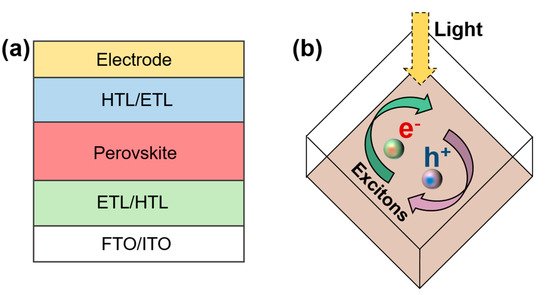
A PSC comprises a positive electrode layer, a hole/electron transport layer, a light absorption layer, an electron/hole transport layer, and a negative electrode layer (
a) [1][13][30][31]. The transport layer transports electrons and holes while preventing them from entering.
a) [1,13,30,31]. The transport layer transports electrons and holes while preventing them from entering.
Figure 3.
(
a
) Structure of PSC and (
b
) schematic diagram of exciton separation.
Perovskite materials have a high dielectric constant and low excitation energy. After absorbing sunlight, the perovskite layer first absorbs photons to generate electron–hole pairs [32][33]. Owing to the difference in the binding energy of excitons in perovskite materials, these carriers either become free carriers or form excitons. (
Perovskite materials have a high dielectric constant and low excitation energy. After absorbing sunlight, the perovskite layer first absorbs photons to generate electron–hole pairs [32,33]. Owing to the difference in the binding energy of excitons in perovskite materials, these carriers either become free carriers or form excitons. ( b). These perovskite materials tend to have a low carrier recombination probability and high carrier mobility; therefore, the diffusion distance and lifetime of the carrier are long. These uncomplexed electrons and holes are collected by the electron transport layer (ETL) and hole transport layer (HTL), respectively, i.e., the electrons are transported from the perovskite layer to the isoelectron transport layer and finally collected by the fluorine-doped tin oxide (FTO). The holes are transported from the perovskite layer to the hole transport layer and are finally collected by the metal electrode.
These processes are accompanied by some carrier losses, such as a reversible recombination of electrons and holes in the ETL and perovskite layer, the recombination of electrons and holes in the ETL and HTL, and the recombination of electrons and holes in the perovskite layer and HTL, respectively. The loss of these carriers should be minimized to improve the overall performance of the device. Finally, a photocurrent is generated through a circuit connecting the FTO and metal electrode [31][34][35]. One of the key methods for improving the PCE of the PSCs is by improving the carrier separation efficiency of the materials.
These processes are accompanied by some carrier losses, such as a reversible recombination of electrons and holes in the ETL and perovskite layer, the recombination of electrons and holes in the ETL and HTL, and the recombination of electrons and holes in the perovskite layer and HTL, respectively. The loss of these carriers should be minimized to improve the overall performance of the device. Finally, a photocurrent is generated through a circuit connecting the FTO and metal electrode [31,34,35]. One of the key methods for improving the PCE of the PSCs is by improving the carrier separation efficiency of the materials.
3. PSC Interface
Several important interfaces exist in a PSC, such as the perovskite/ETL interface and the perovskite/HTL interface. In addition, several important physical processes occur at these interfaces, such as band bending, carrier injection, carrier recombination, charge accumulation, and ion migration. Interface defects contribute significantly to the nonradiative recombination of the interface. The interface between the transport and perovskite layers determines whether the photogenerated carriers can be smoothly transferred from the light-absorption layer to the n/p-type semiconductor [13][29][36][37]. The recombination of charges at the interface severely restricts the photovoltaic performance of PSCs.
Several important interfaces exist in a PSC, such as the perovskite/ETL interface and the perovskite/HTL interface. In addition, several important physical processes occur at these interfaces, such as band bending, carrier injection, carrier recombination, charge accumulation, and ion migration. Interface defects contribute significantly to the nonradiative recombination of the interface. The interface between the transport and perovskite layers determines whether the photogenerated carriers can be smoothly transferred from the light-absorption layer to the n/p-type semiconductor [13,29,36,37]. The recombination of charges at the interface severely restricts the photovoltaic performance of PSCs.
3.1. Interfacial Band Arrangement of PSCs
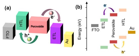
The problem of energy level matching between the interface material and the perovskite is essential for the development of a better PSC. Electrons and holes pass through each layer and encounter many different interfaces (
a,b) (e.g., the electrons will coincide with the perovskite layer/ETL interface and ETL/negative electrode interface, and the holes will coincide with the perovskite layer/HTL interface and HTL/positive electrode interface) [13]. Whether the electrons and holes can pass through those interfaces smoothly depends significantly on whether the energy levels at the interfaces match. The matching of the interface energy level directly affects the collection efficiency of the carriers and hence the final PCE of the device [38][39]. An imperfect interface energy band arrangement will cause a non-radiative recombination of the interface. Regardless of whether the device has a porous/planar, n–i–p, or p–i–n structure, an optimization of multiple interfaces is required [1][4][15][40]. A perfect interface band arrangement is not only conducive to an efficient charge extraction, transmission, and collection, but is also conducive to reducing the interface charge accumulation and J–V hysteresis [41][42].
a,b) (e.g., the electrons will coincide with the perovskite layer/ETL interface and ETL/negative electrode interface, and the holes will coincide with the perovskite layer/HTL interface and HTL/positive electrode interface) [13]. Whether the electrons and holes can pass through those interfaces smoothly depends significantly on whether the energy levels at the interfaces match. The matching of the interface energy level directly affects the collection efficiency of the carriers and hence the final PCE of the device [38,39]. An imperfect interface energy band arrangement will cause a non-radiative recombination of the interface. Regardless of whether the device has a porous/planar, n–i–p, or p–i–n structure, an optimization of multiple interfaces is required [1,4,15,40]. A perfect interface band arrangement is not only conducive to an efficient charge extraction, transmission, and collection, but is also conducive to reducing the interface charge accumulation and J–V hysteresis [41,42].
Figure 4.
Schematic diagram of charge transfer of (
a
) inverted and (
b
) conventional PSCs.
When materials of different functional layers are in contact with each other to form an interface, energy level bending and a charge transfer may occur, causing the vacuum energy level to no longer be leveled, which affects the energy level matching at the interface. The energy level arrangement is affected by several factors, such as the energy level position of the adjacent interface material, interface defects, ion migration, interface instability, and preparation conditions of the adjacent interface layer [10][29][43]. The introduction of the interface materials into the perovskite interface can significantly affect the interface band arrangement and interface carrier dynamics, thereby increasing the open-circuit voltage or effective carrier injection. The movement direction of the material work function depends mainly on the electron cloud density, dipole moment, space concept, and molecular structure of the interface material [28][44]. Various interface materials have been developed to modify the interface in the PSCs, the construction of gradient wide band gap perovskite components, quantum dots, self-assembled monolayers, wide band gap insulating materials, charge transport materials, and small organic molecules [28][45][46][47][48].
When materials of different functional layers are in contact with each other to form an interface, energy level bending and a charge transfer may occur, causing the vacuum energy level to no longer be leveled, which affects the energy level matching at the interface. The energy level arrangement is affected by several factors, such as the energy level position of the adjacent interface material, interface defects, ion migration, interface instability, and preparation conditions of the adjacent interface layer [10,29,43]. The introduction of the interface materials into the perovskite interface can significantly affect the interface band arrangement and interface carrier dynamics, thereby increasing the open-circuit voltage or effective carrier injection. The movement direction of the material work function depends mainly on the electron cloud density, dipole moment, space concept, and molecular structure of the interface material [28,44]. Various interface materials have been developed to modify the interface in the PSCs, the construction of gradient wide band gap perovskite components, quantum dots, self-assembled monolayers, wide band gap insulating materials, charge transport materials, and small organic molecules [28,45,46,47,48].
3.2. Defects at Interface
Similar to other solar cells, the performance of a PSC is governed by its interface. To investigate a PSC, one must understand and rationally regulate their physical processes. Therefore, similar to a bulk nonradiative recombination, minimizing the interface nonradiative recombination loss is crucial for achieving efficient and stable PSCs without hysteresis [10][49]. It has been widely reported that the efficiency, stability, and hysteresis effects of PSCs are closely associated with the nonradiative recombination dynamics of the interface carriers. The main causes of an interface nonradiative recombination loss are the interface defects, imperfect energy level arrangements, and interface reactions. The bulk defects of most perovskite films are shallow point defects, whereas most of the defects at the interface are deep-level and high-latitude defects (such as surface defects, grain boundary defects, and precipitated phase defects) [28][29][50][51][52].
Similar to other solar cells, the performance of a PSC is governed by its interface. To investigate a PSC, one must understand and rationally regulate their physical processes. Therefore, similar to a bulk nonradiative recombination, minimizing the interface nonradiative recombination loss is crucial for achieving efficient and stable PSCs without hysteresis [10,49]. It has been widely reported that the efficiency, stability, and hysteresis effects of PSCs are closely associated with the nonradiative recombination dynamics of the interface carriers. The main causes of an interface nonradiative recombination loss are the interface defects, imperfect energy level arrangements, and interface reactions. The bulk defects of most perovskite films are shallow point defects, whereas most of the defects at the interface are deep-level and high-latitude defects (such as surface defects, grain boundary defects, and precipitated phase defects) [28,29,50,51,52].
The perovskite film prepared using a traditional low-temperature solution method is typically a polycrystalline film, which is prone to pinholes and defects on the grain boundary or surface [53][54][55]. The defects generated can not only capture photogenerated carriers, limit the diffusion of the carriers, and reduce the lifetime of the carriers, they also cause ion migration and diffusion, ultimately resulting in a decrease in the device stability and efficiency. In this study, the defect density at the interface of a polycrystalline film was one to two orders of magnitude higher than that of the defects inside the film. The interfacial deep-level defects can capture carriers at the heterojunction interface and cause nonradiative recombination losses at the interface, thereby reducing the cell efficiency and stability [42][56]. Carriers trapped by defects and charged ions that migrate from the bulk phase to the surface and grain boundaries will accumulate at the interface, resulting in band bending, changes in the energy level arrangement and built-in electric field, and nonradiative recombination losses at the interface, none of which are conducive to a carrier separation, injection, or transmission [57][58].
The perovskite film prepared using a traditional low-temperature solution method is typically a polycrystalline film, which is prone to pinholes and defects on the grain boundary or surface [53,54,55]. The defects generated can not only capture photogenerated carriers, limit the diffusion of the carriers, and reduce the lifetime of the carriers, they also cause ion migration and diffusion, ultimately resulting in a decrease in the device stability and efficiency. In this study, the defect density at the interface of a polycrystalline film was one to two orders of magnitude higher than that of the defects inside the film. The interfacial deep-level defects can capture carriers at the heterojunction interface and cause nonradiative recombination losses at the interface, thereby reducing the cell efficiency and stability [42,56]. Carriers trapped by defects and charged ions that migrate from the bulk phase to the surface and grain boundaries will accumulate at the interface, resulting in band bending, changes in the energy level arrangement and built-in electric field, and nonradiative recombination losses at the interface, none of which are conducive to a carrier separation, injection, or transmission [57,58].
3.3. Chemical Reaction at Interface
In addition to the band arrangement and defects, the chemical reaction has been proven to cause a nonradiative recombination at the interface [10][59]. An interface reaction is caused either by a direct chemical reaction between the interface materials or the reaction between the ions in the perovskite layer and the charge transport layer or electrode. An interface reaction induced by contact can inhibit ion migration or diffusion by introducing chemically inert functional molecules [60]. Furthermore, it can prevent the occurrence of interfacial chemical reactions. The charge recombination loss in the grains of perovskite films prepared using the current technology is almost negligible. However, several studies have shown that the defect state density of polycrystalline perovskite films is several orders of magnitude higher than that of single-crystal perovskite films. This is primarily because of unavoidable structural defects such as uncoordinated Pb
In addition to the band arrangement and defects, the chemical reaction has been proven to cause a nonradiative recombination at the interface [10,59]. An interface reaction is caused either by a direct chemical reaction between the interface materials or the reaction between the ions in the perovskite layer and the charge transport layer or electrode. An interface reaction induced by contact can inhibit ion migration or diffusion by introducing chemically inert functional molecules [60]. Furthermore, it can prevent the occurrence of interfacial chemical reactions. The charge recombination loss in the grains of perovskite films prepared using the current technology is almost negligible. However, several studies have shown that the defect state density of polycrystalline perovskite films is several orders of magnitude higher than that of single-crystal perovskite films. This is primarily because of unavoidable structural defects such as uncoordinated Pb 2+ at the surface of the polycrystalline perovskite film [61][62]. These defect sites not only capture photogenerated carriers and cause energy loss, they also easily adsorb substances such as moisture and oxygen in the environment, thereby accelerating the degradation of the perovskite film.
at the surface of the polycrystalline perovskite film [61,62]. These defect sites not only capture photogenerated carriers and cause energy loss, they also easily adsorb substances such as moisture and oxygen in the environment, thereby accelerating the degradation of the perovskite film.
Vacancy site defects can result in a much faster ion migration at the grain boundary and surface compared with that in the bulk [63][64][65][66]. Eliminating ion migration paths by passivating bulk and interface defects can effectively inhibit ion migration or diffusion. The interface reaction effectively eliminates the surface defects of semiconductor materials and improves the photoelectric performance of the device. Organic molecules contain “Lewis base” functional groups, such as thiophene, pyridine, mercaptans, and compounds containing carbonyl or cyano groups [67][68][69]. They can coordinate with Pb
Vacancy site defects can result in a much faster ion migration at the grain boundary and surface compared with that in the bulk [63,64,65,66]. Eliminating ion migration paths by passivating bulk and interface defects can effectively inhibit ion migration or diffusion. The interface reaction effectively eliminates the surface defects of semiconductor materials and improves the photoelectric performance of the device. Organic molecules contain “Lewis base” functional groups, such as thiophene, pyridine, mercaptans, and compounds containing carbonyl or cyano groups [67,68,69]. They can coordinate with Pb 2+
on the surface of a perovskite film through a lone pair of electrons, thereby passivating the perovskite film. The interaction between the surface of a perovskite film and the functional groups of the passivation molecule can further passivate the grain boundary, including those that are deep in the substrate. This is an effective method for preventing interface chemical reactions by introducing a suitable layer at the interface to physically separate two interface materials in close contact with each other.