In this study we consider the results on the development and exploration of heterostructured photoactive materials with major attention focused on what are the better ways to form this type of materials and how to explore them correctly. Regardless of what type of heterostructure, metal–semiconductor or semiconductor–semiconductor, is formed, its functionality strongly depends on the quality of heterojunction. In turn, it depends on the selection of the heterostructure components (their chemical and physical properties) and on the proper choice of the synthesis method. Several examples of the different approaches such as in situ and ex situ, bottom-up and top-down, are reviewed. At the same time, even if the synthesis of heterostructured photoactive materials seems to be successful, strong experimental physical evidence demonstrating true heterojunction formation are required. A possibility for obtaining such evidence using different physical techniques is discussed.
- photoactive materials
- heterostructures
- heterojunctions
- photoelectrochemistry
- photocatalysis
- solar energy conversion
1. Introduction
For decades heterogeneous photocatalysis and photoelectrochemistry have attracted significant attention from researchers working in the areas of both fundamental and applied science [1][2][3][4][5][6]. In recent years two major targets have been the focus of practical research: the activity and spectral sensitivity of photoactive materials. Several major approaches have been developed to achieve these targets, such as the creation of new photoactive materials, the physical and chemical modification of the known materials to improve their functional properties, and the formation of heterostructures on the basis of known and new materials to create a desired spectral and charge transfer response in the systems [7][8][9][10][11][12][13][14][15][16][17][18]. In recent years significant progress in the development of photoactive materials has been demonstrated in studies devoted to the design, characterization, exploration and application of various heterostructured materials [19][20][21][22][23][24]. In our studyreview we consider the results of the development and exploration of heterostructured photoactive materials, with major attention focused on which are the better ways to form these materials and how to explore them correctly.
Here we denote a heterostructured photoactive material as an object possessing at least one heterojunction between two different components. In typical cases of polycrystalline photoactive materials, such solids as metals, semiconductors and dielectrics can be considered as components of heterostructures. At least one of the components must be a semiconductor (or dielectric) that provides a condition for sufficiently long life-time for the excited state of the heterostructure which is necessary to initiate a further chemical sequence. The AB heterostructures can be classified based on the configuration and dimensions of the interface between two components, A and B, as follows (see Figure 1): one-dimensional (1D), two-dimensional (2D) and three-dimensional (3D) heterostructures [25][26][27][28][29][30][31].
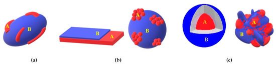
Figure 1. Schemes of 1D (a), 2D (b) and 3D (c) heterostructures.
In a one-dimensional heterostructure, the interface is of line-like shape, that is, the contact area is extended in one direction and not expanded in two others. In this case, the particles (agglomerate of particles) of the same type forming the 1D structure, are separated from each other by another component in heterostructure. Typically, such heterostructured materials are formed with inclusions of nanowires, nanorods, nanotubes, nanofibers, etc. (Figure 1a).
Two-dimensional heterostructures have a plane-like interface between the particles of the components A and B. The dimension of the 2D heterojunction is more extended than the particle sizes of the one or both heterostructure components, and particles of the same type(s) form the layer(s) (Figure 1b). This is typical for planar heterostructures such as “layer-by-layer” systems. A distinguishing feature of the planar heterostructure is that the outer layer of the first component of heterostructure completely covers an inner layer of another component of heterostructure, which means that only the component forming the outer layer contacts with environmental media. This particular case is a formation of photoelectrochemical electrodes when photoactive a semiconductor layer is formed on conductive metal or semiconductor substrates (see Figure 1b, right image). Another possible structure of 2D heterostructure is a so called deposited heterostructure. In this case, both the substrate and the deposited components are in contact with the environment.
The interface of three-dimensional heterostructures extends in all three directions and can be described as a 3D surface of rather complex shape (Figure 1c). This type of heterostructured material is the most common and typically includes powdered (nanoparticle based) components. An illustrative example of a three-dimensional heterosystem is a core-shell structure. However, more typically, particles of such composite materials are the agglomerates of nano- or microcrystallites in contact with each other in different components of heterostructures. In more complex scenarios, 1D and 2D heterostructures can be structural elements of 3D heterostructures. Such systems are very diverse in structure and morphology; this, in turn, makes them unique in terms of their physicochemical properties, photocatalytic and photoelectochemical performance.
Though the family of heterostructured photoactive materials is very broad and diversified, most of the attention is given to metal–semiconductor and semiconductor–semiconductor heterostructures realizing type II and/or Z-scheme heterojunctions (see Figure 2).
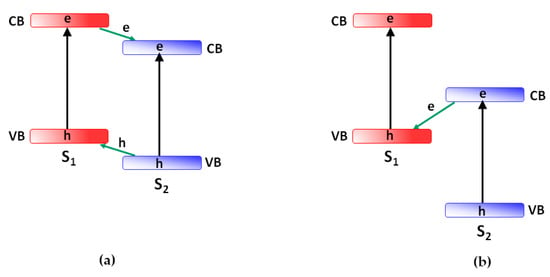
Figure 2. Energy diagrams of heterostructures between two semiconductors (S1 and S2) of type-II (a) and Z-scheme (b).
2. How Photoactive Heterostructures Are Made
In general, heterostructured photoactive materials can be divided into two major types: dispersed and deposited on various substrates (in particular, surfaces such as planar structures). Figure 3 demonstrates various heterostructured photoactive materials. The designs of these materials can be very unusual in form and composition. The heterostructured systems shown in Figure 3a–j represent the dispersed materials, and those in Figure 3k,l have a planar structure. Typically, dispersed photoactive materials are widely used in photocatalytic processes (such as water and air purification, disinfection, the recovery of metals from industrial wastewater and artificial photosynthesis) while deposited (planar) heterostructures are usually used as electrodes in photoelectrochemical systems, including fuel and solar cells. The latter can be used also as self-cleaning coatings.
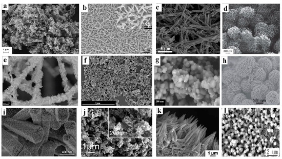
Figure 3. SEM images of the heterostructured materials with various morphology: (a) ZnO nanoparticles on Bi2S3 nanoplates (reproduced from [32]); (b) BiVO4 nanofilm on CuWO4 nanoflowers (reproduced from [33]); (c) BiVO4 nanosheets on AgVO3 nanobelts (reproduced from [34], Elsevier permission); (d) “core-shell” structure Fe3O4@MgAl layered double hydroxides (reproduced from [35], RSC permission); (e) Bi2WO6 nanoplates on the TiO2 nanofiber mat (reproduced from [36], ACS permission); (f) CdS nanoparticles in combination with TiO2 nanorods (from [37]); (g) Ag nanoparticles (appearing as white bright spheres) on agglomerated spherical TiO2 particles (reproduced from [38]); (h) flowerlike crumpled MoS2 nanosheets on CdS particles form nanoflowers (reproduced from [39]); (i) SnO2 nanoparticles on ZnO nanorods grown on glass fiber membrane (reproduced from [40]); (j) CdS nanoparticles on MoS2 nanosheets (reproduced from [41]); (k) layer of lamellar α-Fe2O3 on Co3O4 nanoneedle arrays grown on Ni foam (reproduced from [42]); (l) NiO nanofilm on ZnO nanorods electrodeposited on ITO-coated glass (reproduced from [43]). Systems (a‒j) are dispersed while systems (k) and (l) are planar.
The synthesis and heterostructure formation methods for the dispersed and deposited systems can be significantly different. Further, we consider the major methods of the synthesis and formation of heterostructured materials, indicating for which system they are more suitable.
Photoactive heterostructured materials can be formed via either one-pot (in situ) or multistep (ex situ) synthesis approaches. In the ex situ synthetic strategy (Figure 4a), the components of the heterostructured material are prepared separately in advance and then heterostructures are formed using a variety of techniques such as high temperature solid phase synthesis, drop-casting, sonication assembly, impregnation, ball-milling, sol–gel, or hydrothermal/solvothermal assembly methods, etc. An ex situ synthesis approach has many advantages including low cost and scalable production. However, the methods require multiple complex and time-consuming steps to prepare the individual materials and components of heterostructures. Moreover, it is difficult to control the preparation of the heterostructures, since their components are randomly dispersed with weak interactions. In these cases, it is imperative to verify the quality of the heterojunctions.
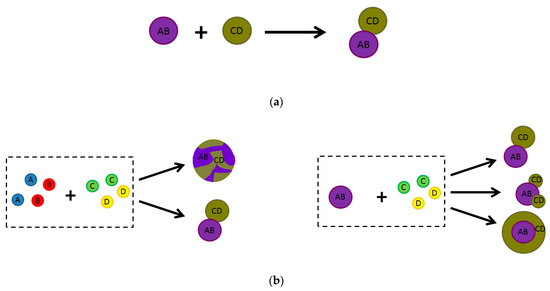
Figure 4. Examples of (a) ex situ and (b) in situ (one-pot) synthetic routes of two-component composite materials of various configurations. AB and CD represent the first and second components of the two-component composite, and A, B, C and D are the components’ precursors.
For an in situ synthesis strategy, the starting materials for one or all of the components of the desired heterostructure are mixed together for further treatment (Figure 4b). Since the synthesis process typically involves ionic reactions, this synthesis route leads to complex interactions and a uniform dispersion of components throughout the entire volume of the heterostructured material. That is why the one-pot synthetic strategy has attracted great attention from researchers in various fields of science, including material science and photocatalysis.
Methods for the synthesis of both heterostructured materials and their individual components can be classified in different ways. For example, all methods can be divided in two groups based on the type of nanostructure formation: the “bottom-up” approach is characterized by the growth of nanoparticles or the assembly of nanoparticles from individual atoms, and the methods related to the group “top-down” are based on the “crushing” of starting materials to nanosized particles or on the intercalation and exfoliation of nanosheets [20][38][44]. Several synthesis methods according to this classification and the possible types of the obtained nanostructures are presented in Table 1. “Top-down” approach methods are able to produce large amounts of nanostructured materials. However, controlling the size of the obtained nanomaterials is very difficult and expensive. The “bottom-up” approach takes advantage of physicochemical interactions for the hierarchical synthesis of ordered structures through a self-assembly of the building blocks. In this approach, particle morphology and size can be easily controlled. For example, graphene- and metal dichalcogenide-based layered composites are successively produced by exfoliation methods [45][46][47][48].
Table 1. Methods for the synthesis of nanomaterials according to the classification “bottom-up” and “top-down”.
| Method Group | Synthesis Method | Type of Materials (Systems) |
|---|---|---|
| “bottom-up” | direct self-assembly | 1D, 2D (QDs, dispersed) |
| layer-by-layer assembly | 2D (dispersed) | |
| emulsion-based synthesis | ||
| colloid-chemical routes | 1D (nanosized dispersed) | |
| thermal decomposition | 2D, 3D (dispersed, planar) | |
| hydrothermal / solvothermal | 1D, 2D, 3D (dispersed, planar) | |
| sol–gel | 2D, 3D (dispersed, planar) | |
| template-directed synthesis | 3D (dispersed) | |
| microwave-assisted | 1D (QDs, dispersed) | |
| laser (photo) ablation | 1D, 2D (QDs, planar) | |
| deposition methods(ALD, PVD, CVD, magnetron sputtering, epitaxy, plasma-enhanced deposition, etc.) | 2D (planar) | |
| “top-down” | mechanical impact (ball milling, gridding, shaking, etc.) | 3D (dispersed) |
| exfoliation methods (in situ ion-exchange or ion intercalation assisted, ultrasonic-assisted, etc.) | 2D (nanosized planar) | |
| techniques based on photolithography, nanoparticle lithography | 1D, 2D (surface nanostructures) | |
| scanning probe lithographic techniques | 1D, 2D (surface nanostructures, up to subnanometers) | |
| chemical etching | 1D, 2D (surface nanostructures) |
The major characteristics for another type of classification is based on the principles for producing and stabilizing a material [27]. According to this classification, synthesis methods can be conventionally divided into three groups: chemical, physical, and mechanical. However, clear borders between these groups do not exist. Thus, the mechanical methods ascribed elsewhere [27][49][50][51][52][53] are often proposed to be combined with chemical methods, and also used for the modification and activation of synthesized materials. Using mechanochemistry, particles with sizes of up to submicron (100–1000 nm) can be produced.
The application of the physical methods for material formation assumes that no new compounds are formed from precursors, although chemical bonds are formed during the growth of the nanostructures. Most physical methods are based on a “top-down” approach (see Table 1) [27]. Various types of lithography are intensively used for nanostructure fabrication [28][44][54][55]. Among the “bottom-up” physical methods, typical examples are molecular beam epitaxy and various methods of evaporation (physical vapor deposition (PVD), magnetron sputtering, plasma-enhanced deposition, laser ablation, electric arc deposition, etc.) followed by growth control in an inert atmosphere and the stabilization of the nanoparticles [45][53]. At the same time, it should be noted that when the particle growth occurs in an active gaseous atmosphere (for example, in the presence of oxygen to obtain oxide nanoparticles), then various chemical reactions can take place. Thus, such processes of material formation start from physical pathways and finish as a chemical reaction. The application of a “bottom-up” approach looks quite attractive, since self-assembly processes open up the possibility of forming rather large arrays of identical elements, and the size of these elements can vary within a wide range (for example, compared to what is currently available in lithography). However, the application of self-assembly processes has at least one drawback, such as packaging defects in the deposited particle layers.
Purely chemical methods involve chemical synthesis routes in which new substances are formed from their precursors. Widely used examples of chemical methods are sol–gel synthesis (including film formation by dip-coating and spin-coating methods from sols), synthesis in micelles (microemulsion approach), high temperature solid-state reaction, chemical precipitation or coprecipitation, chemical bath deposition, etc., i.e., facile methods of wet chemistry. These methods are reviewed in detail elsewhere [26][27][28][29][44][48][51][53]. Chemical precipitation carried out in an aqueous solution is straightforward and readily upgraded to an industrial scale [56][57][58]. However, as precipitation occurs in the entire volume, not all particles come into contact with the substrate. It also causes a wide particle size distribution and poor crystallinity that relies on additional processes such as solvothermal treatment. Hot injection produces particles with a narrow size distribution, but which need further professing to remove the stabilizers and/or organic linkers [59]. Chemical bath deposition is a method best suited for producing one-dimensional structures that have the advantage of increased surface area [60]. Unfortunately, this method is rather limited to several compounds and cannot be used for complex compositions. Summarizing all of the above, the advantages of the chemical methods include their simplicity and scalability, as well as their compatibility with a wide set of nanostructured compounds.
The most widespread methods applied to form heterostructures are physicochemical, in which nanoparticles are formed as a result of chemical reactions under the influence of various “physical” factors such as temperature, pressure, ultrasound and microwave irradiation, etc. These factors affect primarily the thermodynamic and kinetic parameters of the chemical process, but not the substances themselves. This results in the formation of materials with a specific microstructure, phase composition, and consequently, with unique functional properties. Remarkably, it is impossible to obtain a material with such properties carrying out a reaction without an appropriate “physical” impact (for example, see [28][61][62]).
This group includes solvothermal synthesis (sometimes ultrasound-assisted) [27][28][44][51][53][63], microwave-assisted synthesis [26][27][28][44][53], photodeposition [29][44][64], synthesis in supercritical solvents [65], aerosol pyrolysis (spray pyrolysis and laser pyrolysis) [26][27][53][66], chemical exfoliation [53], and methods for nanoparticle or film growth from the gas phase (chemical vapor deposition [26][27][44][51][53][67], atomic layer deposition [48], etc.), the growth of nanostructures by the liquid-crystal mechanism (hot injection [29], successive ionic layer adsorption (SILAR) [29][68] and other methods of layer-by-layer deposition [26][28][44][69]).
Therefore, one can infer that the formation of heterostructured materials with high-quality heterojunctions typically requires a combination of the various methods and techniques (even for in situ synthesis). The selection of the appropriate synthesis method can produce heterostructures with the desired performance. To solve specific synthetic problems, one can be guided by previously accumulated experience (for example, the preparation of mixed-phase heterostructured photocatalysts has already been described for TiO2 [70] and BiVO4 [71]). Today, the scientific literature contains excellent reviews on the synthesis of various heterostructures based on different metal oxides and chalcogenides [28][29][72], hematite [73], layered double hydroxides [74], graphene [45][46][47][48], and quantum dots [65][75].
In the set of various physicochemical methods, electrochemical deposition takes a special place [29][44][53]. It involves chemical reactions in an electrolyte solution when a potential bias is applied to the conducting substrates (metal, FTO or ITO glass). Electrochemical deposition is relatively simple and scalable for the production of planar systems with high-quality heterojunctions in a controllable and directed way. Electrodeposition can be used to form heterostructures with complex morphologies in a highly controllable manner, though it requires an advanced deposition setup.
The fabrication of some hierarchical composite structures, such as core-shell [26][44][66][76] and hollow [44][77] structures, requires an application of the specialized synthetic techniques. The template-assisted method is worth mentioning [44][78]. The employed materials in template synthesis can be simply classified into hard templates (anodic aluminum oxide or silica, possessing well-confined void, which is in the form of channels, pores, or connected hollow space) and soft (consists of organic surfactants, polymers, and even biological viruses, which are relatively flexible in shape) templates. Figure 5 shows some typical examples of the hard and soft template synthesis of electrode materials with diverse morphologies. The overall process generally involves the following procedures: (1) precursors combine with templates by impregnation or incorporation; (2) solid species form through reaction, nucleation and growth; and (3) product is obtained after template removal. Templates can be employed for various synthetic techniques such as sol–gel synthesis, chemical vapor deposition, thermal decomposition, electrodeposition, solvothermal preparation, and so on.
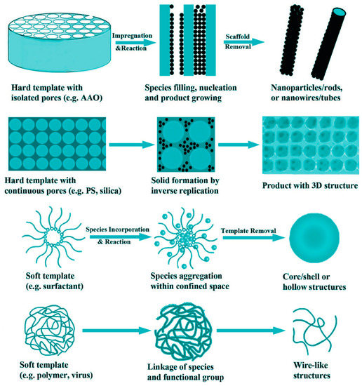
Figure 5. Schematic illustration showing some typical examples of the hard and soft template synthesis. AAO, Anodic aluminum oxide; PS, polystyrene. Reproduced from [78], ACS permission.
Recently [79], a simple, low-cost, versatile, and potentially scalable casting method was proposed for the fabrication of micro- and nanofilms, termed ultrasonic “substrate vibration-assisted drop casting”. Imposing ultrasonic vibration on the substrate can convert the uncontrollable drop casting method into a controllable coating process. Figure 6 illustrates the scheme of the suggested technique. The maximum effective and uniform surface area that can be obtained for application in a device depends on the surface wettability, solution properties, impingement conditions, and substrate vibration.
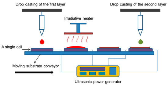
Figure 6. Schematic of proposed automated manufacturing apparatus incorporating ultrasonic substrate vibration-assisted drop casting for the fabrication and heat treatment of solar cell arrays. Reproduced from [79].
It is wise to note that the quality of the resulting heterostructured material, both in dispersed and in deposited form, is significantly affected by such factors as the affinity of heterostructure components (the values of surface free energy, adhesion, surface wettability) [44][55][80], the roughness of the substrate or previously formed layer or component, the formation of the intermediate layer between different components [81], the acidic–basic conditions of the reaction media (especially for the components of heterostructure with different points of zero charge) [29][64][71], the reaction temperature [24][82], the organic binder, surfactant and organic solvent (mainly in the synthesis from solutions, for example, in solvothermal technology) [76][80][82][83][84], etc.
The effect of the reaction temperature on the morphology of monolayer MoS2-WS2 lateral heterostructures has been demonstrated by Liu and coauthors [24]. It was convincingly shown that the size of as-formed heterostructures synthesized via the chemical vapor deposition method proportionally increases with the reaction temperature, which can be explained by the enhanced vapor pressure and reactivity of precursors at elevated temperature. Thus, at the precursor weight ratio (MoO3:WO3) of 1:100, a large size of lateral heterostructure of about 560 µm was obtained at a high temperature of 750 °C. At reaction temperatures above 800 °C, the WS2 stripe embedded in the MoS2 matrix was formed, opening up an easy way for the fabrication of quantum well structures.
The acidity of the reaction medium as an example of influencing factor, is considered below [29]. An optimal pH value for heterostructure formation can be found by measuring the point of zero charge or the ζ-potential value of individual nanoparticles at different pH. Figure 7 demonstrates ζ-potentials of g-C3N4 and Zn2GeO4 nanoparticles in water as a function of acetic acid concentration. As one can see, at a given acid concentration materials exhibit distinct (either positive or negative) ζ-potentials. The region where nanoparticles have opposite charge is then considered as an optimal condition for aggregation.
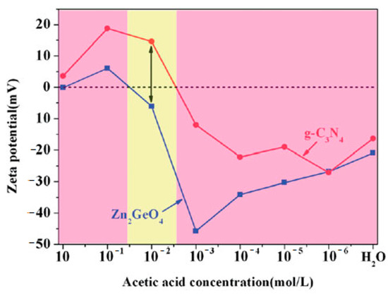
Figure 7. ζ-potentials of g-C3N4 (red line) and Zn2GeO4 (blue line) dispersed as nanoparticles in different acetic acid concentrations. Both g-C3N4 and Zn2GeO4 carry an opposite charge in acetic acid concentrations shown in the yellow zone. Reproduced from [29].
Finally, it is worth mentioning the scaling issues for some synthesis methods. Many of the “bottom-up” methods for the synthesis of nanomaterials are based on solution synthesis, in which precursor concentrations are usually very low (typically, in the millimolar range). Scaling up these synthesis approaches to produce commercial-scale quantities is expected to introduce significant challenges for control of particle size, morphology, and structure. This aspect of nanomaterial synthesis is still in its infancy and offers new exciting research endeavors in the area of photoactive heterostructured materials.
3. Conclusions
In conclusion, it should be emphasized that in order to improve the physical properties of heterostructures, the key issues are the design and synthesis of complex heterostructures with controlled assembly of each section of materials, including the size, shape, and uniformity of the building blocks. This control can be achieved by the exploration and variation of the kinetic and thermodynamic parameters of synthesis processes. A fundamental understanding of the nucleation and growth mechanisms as well as the unidirectional growth of crystal facets could be highly desirable for the development of effective heterostructured photoactive materials and the devices based on them. There is strong demand for standard or unique synthesis approaches with large yields, uncontaminated heterostructures, and minimal aggregation effects. At the same time, quality control of heterojunctions and systematic comparative studies of the heterostructured materials and their components using electrophysical methods are necessary to prove the formation of heterostructures and to understand their functional actions. Unfortunately, the optical methods typically used for the exploration of single component photoactive materials cannot provide reliable information about heterostructure behavior, especially when they are used incorrectly. In fact, a physical mixture of two (or more) components can demonstrate an optical response similar to true heterostructures based on these components. Reliable proof of heterostructure formation requires the application of high-precision microscopic techniques such as HRTEM and electron crystallography due to their outstanding spatial resolution and excellent reproducibility. Quality control of the heterojunctions in the formed heterostructured materials and systematic studies of their functional properties in comparison with heterostructure components should be carried out by electrophysical methods, namely, the Kelvin probe method and EIS spectroscopy.
References
- Chen, X.; Mao, S.S. Titanium dioxide nanomaterials: Synthesis, properties, modifications, and applications. Chem. Rev. 2007, 7, 2891–2959.
- Schneider, J.; Matsuoka, M.; Takeuchi, M.; Zhang, J.; Horiuchi, Y.; Anpo, M.; Bahnemann, D.W. Understanding TiO2 Photocatalysis: Mechanisms and Materials. Chem. Rev. 2014, 114, 9919–9986.
- Fujishima, A.; Hashimoto, K.; Watanabe, T. TiO2 Photocatalysis: Fundamentals and Applications; BKC Publ.: Tokyo, Japan, 1999.
- Graetzel, M. Dye-sensitized solar cells. J. Photochem. Photobiol. C 2003, 4, 145–153.
- Serpone, N.; Emeline, A.V. Fundamentals in metal-oxide heterogeneous photocatalysis. In Nanostructured and Photoelectrochemical Systems for Solar Photon Conversion; Archer, M.D., Nozik, A.J., Eds.; Imperial College Press: London, UK, 2008; pp. 275–381.
- Nakata, K.; Ochiai, T.; Murakami, T.; Fujishima, A. Photoenergy conversion with TiO2 photocatalysis: New materials and recent applications. Electrochim. Acta 2012, 84, 103–111.
- Serpone, N.; Lawless, D.; Disdier, J.; Herrmann, J.M. Spectroscopic, Photoconductivity, and Photocatalytic Studies of TiO2 Colloids: Naked and with the Lattice Doped with Cr3+, Fe3+, and V5+ Cations. Langmuir 1994, 10, 643–652.
- Nagaveni, K.; Hedge, M.S.; Madras, G. Structure and photocatalytic activity of Ti1-xM xO2×δ (M = W, V, Ce, Zr, Fe, and Cu) synthesized by solution combustion method. J. Phys. Chem. B 2004, 108, 20204–20212.
- Gracia, F.; Holgado, J.P.; Caballero, A.; Gonzalez-Elipe, A.R. Structural, Optical, and Photoelectrochemical Properties of Mn+−TiO2 Model Thin Film Photocatalyst. J. Phys. Chem. B 2004, 108, 17466–17476.
- Torres, G.R.; Lindgren, T.; Lu, J.; Granqvist, C.-G.; Lindquist, S.-E. Photoelectrochemical study of nitrogen-doped titanium dioxide for water oxidation. J. Phys. Chem. B 2004, 108, 5995–6003.
- Nakamura, R.; Tanaka, T.; Nakato, Y. Mechanism for visible light responses in anodic photocurrents at N-doped TiO2 film electrodes. J. Phys. Chem. B 2004, 108, 10617–10620.
- Meng, S.; Zhang, J.; Chen, S.H.; Zhang, S.; Huang, W. Perspective on construction of heterojunction photocatalysts and the complete utilization of photogenerated charge carriers. Appl. Surf. Sci. 2019, 476, 982–992.
- Lianos, P. Review of recent trends in photoelectrocatalytic conversion of solar energy to electricity and hydrogen. Appl. Catal. B Environ. 2017, 210, 235–254.
- He, X.; Zhang, C. Recent advances in structure design for enhancing photocatalysis. J. Mater. Sci. 2019, 54, 8831–8851.
- Serpone, N.; Emeline, A.V.; Ryabchuk, V.K.; Kuznetsov, V.N.; Artem’ev, Y.M.; Horikoshi, S. Why do Hydrogen and Oxygen Yields from Semiconductor-Based Photocatalyzed Water Splitting Remain Disappointingly Low? Intrinsic and Extrinsic Factors Impacting Surface Redox Reactions. ACS Energy Lett. 2016, 1, 931–948.
- Yu, J.; Wang, S.; Lowa, J.; Xiao, W. Enhanced photocatalytic performance of direct Z-scheme g-C3N4-TiO2 photocatalysts for the decomposition of formaldehyde in air. Phys. Chem. Chem. Phys. 2013, 15, 16883–16890.
- Low, J.; Jiang, C.; Cheng, B.; Wageh, S.; Al-Ghamdi, A.A.; Yu, J. A Review of Direct Z-Scheme Photocatalysts. Small Methods 2017, 1, 1700080.
- Serpone, N.; Emeline, A.V. Semiconductor Photocatalysis - Past, Present, and Future Outlook. J. Phys. Chem. Lett. 2012, 3, 673–677.
- Enesca, A.; Andronic, L. The Influence of Photoactive Heterostructures on the Photocatalytic Removal of Dyes and Pharmaceutical Active Compounds: A Mini-Review. Nanomaterials 2020, 10, 1766.
- Zhang, R.; Sun, M.; Zhao, G.; Yin, G.; Liu, B. Hierarchical Fe2O3 nanorods/TiO2 nanosheets heterostructure: Growth mechanism, enhanced visible-light photocatalytic and photoelectrochemical performances. Appl. Surf. Sci. 2019, 475, 380–388.
- Ghosh, M.; Liu, J.; Chuang, S.S.C.; Jana, S.C. Fabrication of Hierarchical V2O5 Nanorods on TiO2 Nanofibers and Their Enhanced Photocatalytic Activity under Visible Light. ChemCatChem 2018, 10, 3305–3318.
- Lin, Y.-Z.; Wang, K.; Zhang, Y.; Dou, Y.; Yang, Y.; Xu, M.; Wang, Y.; Liu, F.; Li, K. Metal–organic framework-derived CdS–NiO heterostructures with modulated morphology and enhanced photocatalytic hydrogen evolution activity in pure water. J. Mater. Chem. C 2020, 8, 10071–10077.
- Kaur, N.; Zappa, D.; Ferroni, M.; Poli, N.; Campanini, M.; Negrea, R.; Comini, E. Branch-like NiO/ZnO heterostructures for VOC sensing. Sens. Actuators B Chem. 2018, 262, 477–485.
- Zhou, J.; Tang, B.; Lin, J.; Lv, D.; Shi, J.; Sun, L.; Zeng, Q.; Niu, L.; Liu, F.; Wang, X.; et al. Morphology Engineering in Monolayer MoS2-WS2 Lateral Heterostructures. Adv. Funct. Mater. 2018, 28, 1801568.
- van de Voorde, M.; Tulinski, M.; Jurczyk, M. Engineered Nanomaterials: A Discussion of the Major Categories of Nanomaterials. In Metrology and Standardization of Nanotechnology: Protocols and Industrial Innovations; Mansfield, E., Kaiser, D.L., Fujita, D., van de Voorde, M., Eds.; Wiley-VCH Verlag GmbH & Co. KGaA: Weinheim, Germany, 2017; pp. 49–74.
- Vattikuti, S.V.P. Heterostructured Nanomaterials: Latest Trends in Formation of Inorganic Heterostructures. In Synthesis of Inorganic Nanomaterials; Bhagyaraj, S.M., Oluwafemi, O.S., Kalarikkal, N., Thomas, S., Eds.; Elsevier: Amsterdam, The Netherlands, 2018; pp. 89–120.
- Kulkarni, S.K. Nanotechnology: Principles and Practices; Springer: Berlin/Heidelberg, Germany, 2015; 403p.
- Grabowska, E.; Marchelek, M.; Paszkiewicz-Gawron, M.; Zaleska-Medynska, A. Metal Oxide-Based Photocatalysis; Zaleska-Medynska, A., Ed.; Elsevier: Amsterdam, The Netherlands, 2018; pp. 51–207.
- Šutka, A.; Järvekülg, M.; Gross, K.A. Photocatalytic Nanoheterostructures and Chemically Bonded Junctions Made by Solution-Based Approaches. Crit. Rev. Solid State Mater. Sci. 2019, 44, 239–263.
- Luo, B.; Liu, G.; Wang, L. Recent advances in 2D materials for photocatalysis. Nanoscale 2016, 8, 6904–6920.
- Yuan, Y.-P.; Ruan, L.-W.; Barber, J.; Loo, S.C.J.; Xue, C. Hetero-nanostructured suspended photocatalysts for solar-to-fuel conversion. Energy Environ. Sci. 2014, 7, 3934–3951.
- Yuan, X.; Wu, X.; Feng, Z.; Jia, W.; Zheng, X.; Li, C. Facile Synthesis of Heterojunctioned ZnO/Bi2S3 Nanocomposites for Enhanced Photocatalytic Reduction of Aqueous Cr(VI) under Visible-Light Irradiation. Catalysts 2019, 9, 624.
- Peng, B.; Xia, M.; Li, C.; Yue, C.; Diao, P. Network Structured CuWO4/BiVO4/Co-Pi Nanocomposite for Solar Water Splitting. Catalysts 2018, 8, 663.
- Ju, P.; Wang, Y.; Sun, Y.; Zhang, D. In-Situ Green Topotactic Synthesis of a Novel Z-Scheme 3/BiVO4 Heterostructure with Highly Enhanced Visible-Light Photocatalytic Activity. J. Colloid Interface Sci. 2020, 579, 431–447.
- Mi, F.; Chen, X.; Ma, Y.; Yin, S.; Yuan, F.; Zhang, H. Facile Synthesis of Hierarchical Core–Shell Fe3O4@MgAl– as Magnetically Recyclable Catalysts for Catalytic Oxidation of Alcohols. Chem. Commun. 2011, 47, 12804–12806.
- Shang, M.; Wang, W.; Zhang, L.; Sun, S.; Wang, L.; Zhou, L. 3D Bi2WO6/TiO2 Hierarchical Heterostructure: Controllable Synthesis and Enhanced Visible Photocatalytic Degradation Performances. J. Phys. Chem. C 2009, 113, 14727–14731.
- Kim, H.; Tak, Y.; Senthil, K.; Joo, J.; Jeon, S.; Yong, K. Novel Heterostructure of CdS Nanoparticle/WO3 Nanowhisker: Synthesis and Photocatalytic Properties. J. Vac. Sci. Technol. 2009, 27, 2182.
- Handoko, C.T.; Moustakas, N.G.; Peppel, T.; Springer, A.; Oropeza, F.E.; Huda, A.; Bustan, M.D.; Yudono, B.; Gulo, F.; Strunk, J. Characterization and Effect of Ag(0) vs. Ag(I) Species and Their Localized Plasmon Resonance on Photochemically Inactive TiO2. Catalysts 2019, 9, 323.
- Wang, C.; Lin, H.; Xu, Z.; Cheng, H.; Zhang, C. One-Step Hydrothermal Synthesis of Flowerlike MoS2/CdS Heterostructures for Enhanced Visible-Light Photocatalytic Activities. RSC Adv. 2015, 5, 15621.
- Rogé, V.; Didierjean, J.; Crêpellière, J.; Arl, D.; Michel, M.; Fechete, I.; Dinia, A.; Lenoble, D. Tuneable Functionalization of Glass Fibre Membranes with ZnO/SnO2 Heterostructures for Photocatalytic Water Treatment: Effect of SnO2 Coverage Rate on the Photocatalytic Degradation of Organics. Catalysts 2020, 10, 733.
- He, G.; Zhang, Y.; He, Q. MoS2/CdS Heterostructure for Enhanced Photoelectrochemical Performance under Visible Light. Catalysts 2019, 9, 379.
- Luo, Y.; Kong, D.; Luo, J.; Wang, Y.; Zhang, D.; Qiu, K.; Cheng, C.; Li, C.M.; Yu, T. Seed-Assisted Synthesis of Co3O4@α-Fe2O3 Core–Shell Nanoneedle Arrays for Lithium-Ion Battery Anode with High Capacity. RSC Adv. 2014, 4, 13241.
- Wang, L.; Su, Z.; Yuan, J. The Influence of Materials, Heterostructure, and Orientation for Nanohybrids on Photocatalytic Activity. Nanoscale Res. Lett. 2019, 14, 20.
- Qiao, S.-Z.; Liu, J.; Lu, G.Q.M. Synthetic Chemistry of Nanomaterials. In Modern Inorganic Synthetic Chemistry; Xu, R., Xu, Y., Eds.; Elsevier: Amsterdam, The Netherlands, 2017; pp. 613–640.
- Butler, S.Z.; Hollen, S.M.; Cao, L.Y.; Cui, Y.; Gupta, J.A.; Gutierrez, H.R.; Heinz, T.F.; Hong, S.S.; Huang, J.X.; Ismach, A.F.; et al. Progress, Challenges, and Opportunities in Two-Dimensional Materials Beyond Graphene. ACS Nano 2013, 7, 2898–2926.
- Coleman, J.N.; Lotya, M.; O’Neill, A.; Bergin, S.D.; King, P.J.; Khan, U.; Young, K.; Gaucher, A.; De, S.; Smith, R.J.; et al. Two-Dimensional Nanosheets Produced by Liquid Exfoliation of Layered Materials. Science 2011, 331, 568–571.
- Chen, D.; Chen, W.; Ma, L.; Ji, G.; Chang, K.; Lee, J.Y. Graphene-Like Layered Metal Dichalcogenide/Graphene Composites: Synthesis and Applications in Energy Storage and Conversion. Mater. Today 2014, 17, 184–193.
- Ozer, L.Y.; Garlisi, C.; Oladipo, H.; Pagliaro, M.; Sharief, S.A.; Yusuf, A.; Almheiri, S.; Palmisano, G.J. Inorganic semiconductors-graphene composites in photo (electro) catalysis: Synthetic strategies, interaction mechanisms and applications. Photochem. Photobiol. C Photochem. Rev. 2017, 33, 132–164.
- Boldyrev, V.V. Mechanochemistry and Mechanical Activation of Solids. Rus. Chem. Rev. 2006, 75, 177–189.
- James, S.L.; Adams, C.J.; Bolm, C.; Braga, D.; Collier, P.; Friščić, T.; Grepioni, F.; Harris, K.D.M.; Hyett, G.; Jones, W.; et al. Mechanochemistry: Opportunities for New and Cleaner Synthesis. Chem. Soc. Rev. 2012, 41, 413–447.
- Tulinski, M.; Jurczyk, M. Nanomaterials Synthesis Methods. In Metrology and Standardization of Nanotechnology: Protocols and Industrial Innovations; Mansfield, E., Kaiser, D.L., Fujita, D., van de Voorde, M., Eds.; Wiley-VCH Verlag GmbH & Co. KGaA: Weinheim, Germany, 2017; pp. 75–98.
- Xu, R.-R.; Su, Q. High Temperature Synthesis. In Modern Inorganic Synthetic Chemistry; Xu, R., Xu, Y., Eds.; Elsevier: Amsterdam, The Netherlands, 2017; pp. 9–43.
- Rani, A.; Reddy, R.; Sharma, U.; Mukherjee, P.; Mishra, P.; Kuila, A.; Sim, L.C.; Saravanan, P. A Review on the Progress of Nanostructure Materials for Energy Harnessing and Environmental Remediation. J. Nanostruct. Chem. 2018, 8, 255–291.
- Colson, P.; Henrist, C.; Cloots, R. Nanosphere Lithography: A Powerful Method for the Controlled Manufacturing of Nanomaterials. J. Nanomater. 2013, 948510, 19.
- Xia, Y.N.; Whitesides, G.M. Soft Lithography. Angew. Chem. Int. Ed. 1998, 37, 550–575.
- Phonthammachai, N.; Rumruangwong, M.; Gulari, E.; Jamieson, A.M.; Jitkarnka, S.; Wongkasemjit, S. Synthesis and Rheological Properties of Mesoporous Nanocrystalline CeO2 via Sol–Gel Process. Coll. Surf. A Physicochem. Eng. Asp. 2004, 247, 61–68.
- Tyrpekl, V.; Vejpravová, J.P.; Roca, A.G.; Murafa, N.; Szatmary, L.; Nižňanský, D. Magnetically Separable Photocatalytic Composite γ-Fe2O3@TiO2 Synthesized by Heterogeneous Precipitation. Appl. Surf. Sci. 2011, 257, 4844–4848.
- Sánchez-Martínez, D.; la Cruz, A.M.; López-Cuéllar, E. Synthesis of WO3 Nanoparticles by Citric Acid-Assisted Precipitation and Evaluation of Their Photocatalytic Properties. Mater. Res. Bull. 2013, 48, 691–697.
- Acharya, K.P.; Hewa-Kasakarage, N.N.; Alabi, T.R.; Nemitz, I.; Khon, E.; Ullrich, B.; Anzenbacher, P.; Zamkov, M. Synthesis of PbS/TiO2 Colloidal Heterostructures for Photovoltaic Applications. J. Phys. Chem. C 2010, 114, 12496–12504.
- Aniskevich, Y.M.; Malashchonak, M.V.; Chulkin, P.V.; Ragoisha, G.A.; Streltsov, E.A. Cadmium Underpotential Deposition on CdSe and CdS Quantum Dot Films: Size Dependent Underpotential Shift. Electrochim. Acta 2016, 220, 493–499.
- Cao, S.-W.; Zhu, Y.-J. Iron Oxide Hollow Spheres: Microwave–Hydrothermal Ionic Liquid Preparation, Formation Mechanism, Crystal Phase and Morphology Control and Properties. Acta Mater. 2009, 57, 2154–2165.
- Bang, J.H.; Suslick, K.S. Applications of ultrasound to the synthesis of nanostructured materials. Adv. Mater. 2010, 22, 1039–1059.
- Feng, S.-H.; Li, G.-H. Hydrothermal and Solvothermal Syntheses. In Modern Inorganic Synthetic Chemistry; Xu, R., Xu, Y., Eds.; Elsevier: Amsterdam, The Netherlands, 2017; pp. 73–104.
- Rao, V.N.; Reddy, N.L.; Kumari, M.M.; Cheralathan, K.K.; Ravi, P.; Sathish, M.; Neppolian, B.; Reddy, K.R.; Shetti, N.P.; Prathap, P.; et al. Sustainable Hydrogen Production for the Greener Environment by Quantum Dots-Based Efficient Photocatalysts: A Review. J. Environ. Manag. 2019, 248, 109246.
- Türk, M.; Erkey, C. Synthesis of Supported Nanoparticles in Supercritical Fluids by Supercritical Fluid Reactive Deposition: Current State, Further Perspectives and Needs. J. Supercrit. Fluids 2018, 134, 176–183.
- He, X.; Wang, W.-N. Rational Design of Efficient Semiconductor-Based Photocatalysts via Microdroplets: A Review. KONA Powder Part. J. 2019, 36, 201–214.
- Wang, J.-T. Chemical Vapor Deposition and Its Applications in Inorganic Synthesis. In Modern Inorganic Synthetic Chemistry; Xu, R., Xu, Y., Eds.; Elsevier: Amsterdam, The Netherlands, 2017; pp. 167–188.
- Korotcenkov, G.; Tolstoy, V.; Schwank, J. Successive Ionic Layer Deposition (SILD) as a New Sensor Technology: Synthesis and Modification of Metal Uxides. Meas. Sci. Technol. 2006, 17, 1861–1869.
- Tolstoi, V.P. New Routes for the Synthesis of Nanocomposite Layers of Inorganic Compounds by the Layer-by-Layer Scheme. Rus. J. Gen. Chem. 2009, 79, 2578–2583.
- Chalastara, K.; Guo, F.; Elouatik, S.; Demopoulos, G.P. Tunable Composition Aqueous-Synthesized Mixed-Phase TiO2 Nanocrystals for Photo-Assisted Water Decontamination: Comparison of Anatase, Brookite and Rutile Photocatalysts. Catalysts 2020, 10, 407.
- Nguyen, T.D.; Nguyen, V.-H.; Nanda, S.; Vo, D.-N.; Nguyen, V.H.; Tran, T.V.; Xuan, L.N.; Nguyen, T.T.; Bach, L.-G.; Abdullah, B.; et al. BiVO4 Photocatalysis Design and Applications to Oxygen Production and Degradation of Organic Compounds: A Review. Environ. Chem. Lett. 2020.
- Sudha, D.; Sivakumar, P. Review on the Photocatalytic Activity of Various Composite Catalysts. Chem. Eng. Process. 2015, 97, 112–133.
- Wu, W.; Jiang, C.; Roy, V.A.L. Recent Progress in Magnetic Iron Oxide–Semiconductor Composite Nanomaterials as Promising Photocatalysts. Nanoscale 2015, 7, 38–58.
- Prasad, C.; Tang, H.; Liu, Q.Q.; Zulfiqar, S.; Shah, S.; Bahadur, I. An Overview of Semiconductors/Layered Double Hydroxides Composites: Properties, Synthesis, Photocatalytic and Photoelectrochemical Applications. J. Molec. Liquids 2019, 289, 111114.
- Chu, K.-W.; Lee, S.L.; Chang, C.-J.; Liu, L. Recent Progress of Carbon Dot Precursors and Photocatalysis Applications. Polymers 2019, 11, 689.
- Gawande, M.B.; Goswami, A.; Asefa, T.; Guo, H.; Biradar, A.V.; Peng, D.-L.; Zboril, R.; Varma, R.S. Core–Shell Nanoparticles: Synthesis and Applications in Catalysis and Electrocatalysis. Chem. Soc. Rev. 2015, 44, 7540–7590.
- Wang, S.; Wang, Y.; Zang, S.-Q.; Lou, X.W. Hierarchical Hollow Heterostructures for Photocatalytic CO2 Reduction and Water Splitting. Small Methods 2019, 4, 1900586.
- Cheng, F.; Tao, Z.; Liang, J.; Chen, J. Template-Directed Materials for Rechargeable Lithium-Ion Batteries. Chem. Mater. 2008, 20, 667–681.
- Eslamian, M.; Zabihi, F. Ultrasonic Substrate Vibration-Assisted Drop Casting (SVADC) for the Fabrication of Photovoltaic Solar Cell Arrays and Thin-Film Devices. Nanoscale Res. Let. 2015, 10, 462.
- Tolstoy, V.P. Successive Ionic Layer Deposition. The Use in Nanotechnology. Rus. Chem. Rev. 2006, 75, 161–175.
- Erkov, V.G.; Devyatova, S.F.; Molodstova, E.L.; Malsteva, T.V.; Yanovskii, U.A. Si–TiO2 Interface Evolution at Prolonged Annealing in Low Vacuum or N2O Ambient. Appl. Surf. Sci. 2000, 166, 51–56.
- Chen, B.; Meng, Y.; Sha, J.; Zhong, C.; Hua, W.; Zhao, N. Preparation of MoS2/TiO2 Based Nanocomposites for Photocatalysis and Rechargeable Batteries: Progress, Challenges, and Perspective. Nanoscale 2018, 10, 34–68.
- Zori, M.H. Synthesis of TiO2 Nanoparticles by Microemulsion/Heat Treated Method and Photodegradation of Methylene Blue. J. Inorg. Organomet. Polym. 2011, 21, 81–90.
- Rivera-Gonzalez, N.; Chauhan, S.; Watson, D.F. Aminoalkanoic Acids as Alternatives to Mercaptoalkanoic Acids for the Linker-Assisted Attachment of Quantum Dots to TiO2. Langmuir 2016, 32, 9206–9215.