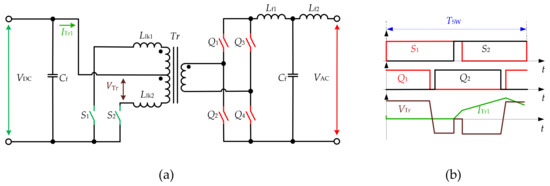
This entry addresses the topologies of the single-stage isolated matrix inverters with a grid-side switching stage based on the current source inverter (CSI). These inverters have been proposed for the uninterruptible power supplies, high and low-voltage/power photovoltaic systems, low-power fuel cell, different low- and high-voltage battery and/or electric vehicle chargers, audio amplifiers. The fully controlled switches on both terminals of these converters typically can provide the bidirectional power transfer capability, which is also addressed for most of the topologies. The other advantages include soft-switching of semiconductors and absence of the bulky DC-link capacitor. Average efficiency of today’s isolated matrix inverters is comparable with the two-stage power converters; however, due to absence of DC-link they can provide higher reliability and lower cost.
- isolated matrix inverter
- current source inverter
- bridge
- push–pull
- modulation methods
- soft switching
CSI Based Isolated Matrix Topologies
Full Bridge Configuration
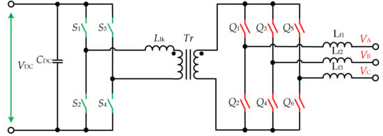
Full Bridge Configuration with Three Legs at the DC Side
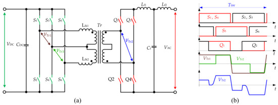
Full Bridge Configuration with the Reconfigurable AC Side
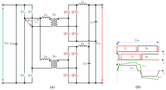
The Full Bridge Configuration with Push-Pull at the DC Side
Half Bridge Configuration

LL (dual inductor) HB Configuration
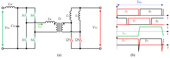
Non-Resonant Push-Pull Topologies
Push-Pull Configuration

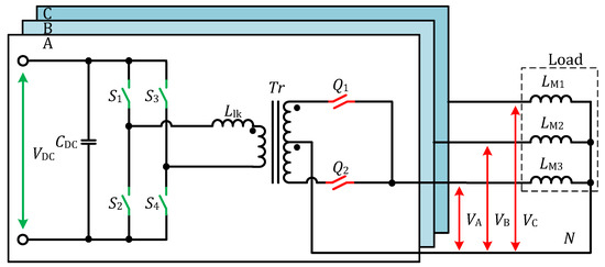
Push-Pull Configuration with voltage clamper
Push-Pull Configuration with the Current Clamping Switch
Resonant Push-Pull Topologies
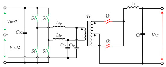
Push-Pull Configuration with a Parallel Resonant Tank at the DC Side
- Mennicken, H. Stromrichtersystem Mit Wechselspannungs-Zwischenkreis Und Seine Anwendung in der Traktionstechnik. Ph.D. Thesis, RWTH Aachen University, Aachen, Germany, 1978. [Google Scholar]
- Kawabata, T.; Honjo, K.; Sashida, N.; Sanada, K.; Koyama, M. High frequency link DC/AC converter with PWM cycloconverter. In Proceedings of the Conference Record of the 1990 IEEE Industry Applications Society Annual Meeting, Seattle, WA, USA, 7–12 October 1990; Volume 2, pp. 1119–1124. [Google Scholar]
- Matsui, M.; Nagai, M.; Mochizuki, M.; Nabae, A. High-frequency link DC/AC converter with suppressed voltage clamp circuits-naturally commutated phase angle control with self turn-off devices. IEEE Trans. Ind. Appl. 1996, 32, 293–300. [Google Scholar] [CrossRef]
- Krishnaswami, H. Photovoltaic microinverter using single-stage isolated high-frequency link series resonant topology. In Proceedings of the 2011 IEEE Energy Conversion Congress and Exposition, Phoenix, AZ, USA, 17–22 September 2011; pp. 495–500. [Google Scholar]
- Surapaneni, R.K.; Yelaverthi, D.B.; Rathore, A.K. Cycloconverter-Based Double-Ended Microinverter Topologies for Solar Photovoltaic AC Module. IEEE J. Emerg. Sel. Top. Power Electron. 2016, 4, 1354–1361. [Google Scholar] [CrossRef]
- Mazumder, S.K.; Burra, R.K.; Huang, R.; Tahir, M.; Acharya, K. A Universal Grid-Connected Fuel-Cell Inverter for Residential Application. IEEE Trans. Ind. Electron. 2010, 57, 3431–3447. [Google Scholar] [CrossRef]
- Krein, P.; Balog, R.; Geng, X. High-Frequency Link Inverter for Fuel Cells Based on Multiple-Carrier PWM. IEEE Trans. Power Electron. 2004, 19, 1279–1288. [Google Scholar] [CrossRef]
- Iyer, K.; Mohan, N. Modulation and Commutation of a Single Stage Isolated Asymmetrical Multilevel Converter for Integration of Renewables and Battery Energy Storage System in Ships. IEEE Trans. Transp. Electrif. 2016, 2, 1. [Google Scholar] [CrossRef]
- Norrga, S. A soft-switched bi-directional isolated AC/DC converter for AC-fed railway propulsion applications. In Proceedings of the 2002 International Conference on Power Electronics, Machines and Drives, Sante Fe, NM, USA, 4–7 June 2002; pp. 433–438. [Google Scholar]
- Jauch, F.; Biela, J. Single-phase single-stage bidirectional isolated ZVS AC-DC converter with PFC. In Proceedings of the 2012 15th International Power Electronics and Motion Control Conference (EPE/PEMC), Novi Sad, Serbia, 4–6 September 2012. [Google Scholar]
- Basu, K.; Mohan, N. A High-Frequency Link Single-Stage PWM Inverter With Common-Mode Voltage Suppression and Source-Based Commutation of Leakage Energy. IEEE Trans. Power Electron. 2013, 29, 3907–3918. [Google Scholar] [CrossRef]
- Alluhaybi, K.; Batarseh, I.; Hu, H.; Chen, X. Comprehensive Review and Comparison of Single-Phase Grid-Tied Photovoltaic Microinverters. IEEE J. Emerg. Sel. Top. Power Electron. 2020, 8, 1310–1329. [Google Scholar] [CrossRef]
- Fornage, M.; Hassan-Ali, M.; Omar, T.H. Method and Apparatus for Providing Power Conversion Using an Interleaved Flyback Converter with Automatic Balancing. Patent EP2043246A2, 2007. Available online: https://patents.google.com/patent/EP2043246A2/ru (accessed on 9 May 2020).
- Harrison, M.J.; Zimmanck, D.R. Single-Phase Cycloconverter with Integrated Line-Cycle Energy Storage. Patent WO2015038995A1, 2014. Available online: https://patents.google.com/patent/WO2015038995A1/en?oq=WO2015038995A1 (accessed on 9 May 2020).
- Kimball, J.W.; Krein, P.T.; Benavides, N.D. Modular System for Unattended Energy Generation and Storage. Patent US8350411B2, 2006. Available online: https://patents.google.com/patent/US8350411B2/en (accessed on 9 May 2020).
- Kwon, O.; Kim, J.; Kwon, J.-M.; Kwon, B.-H. Bidirectional Grid-Connected Single-Power-Conversion Converter With Low-Input Battery Voltage. IEEE Trans. Ind. Electron. 2017, 65, 3136–3144. [Google Scholar] [CrossRef]
- Chen, W.W.; Zane, R.; Corradini, L. Isolated Bidirectional Grid-Tied Three-Phase AC–DC Power Conversion Using Series-Resonant Converter Modules and a Three-Phase Unfolder. IEEE Trans. Power Electron. 2017, 32, 9001–9012. [Google Scholar] [CrossRef]
- Diogo, A.C.P.B.V.; Luís, M.F.M.; Rui, M.E.A. Single-Phase Cycloconverter with Integrated Line-Cycle Energy Storage. Patent US9973107B2, 2015. Available online: https://patents.google.com/patent/US9973107B2/en (accessed on 9 May 2020).
- Guo, S.; Su, J.; Guo, L.; Chen, X. Phase-shifted modulation strategies for a single-stage isolated bi-directional power amplifier. In Proceedings of the 2016 IEEE 8th International Power Electronics and Motion Control Conference (IPEMC-ECCE Asia), Hefei, China, 22–26 May 2016; pp. 1206–1211. [Google Scholar]
- Norrga, S.; Meier, S.; Ostlund, S. A three-phase soft-switched isolated AC/DC converter without auxiliary circuit. IEEE Trans. Ind. Appl. 2004, 44, 836–844. [Google Scholar] [CrossRef]
- Vangen, K.; Melaa, T.; Bergsmark, S.; Nilsén, R. Efficient high-frequency soft-switched power converter with signal processor control. In Proceedings of the Thirteenth International Telecommunications Energy Conference—INTELEC 91, Kyoto, Japan, 5–8 November 1991; pp. 631–639. [Google Scholar]
- Aganza-Torres, A.; Cardenas, V. Analysis and modelling of HF-Link Cycloconverter based inverter for low-power renewable energy sources applications. In Proceedings of the 2011 8th International Conference on Electrical Engineering, Computing Science and Automatic Control, Merida City, Mexico, 26–28 October 2011; pp. 1–6. [Google Scholar]
- Kummari, N.; Chattopadhyay, S. Three-Legged High-Gain Phase-Modulated DC–AC Converter for Mitigation of Device Capacitance Induced Ringing Voltage. IEEE Trans. Power Electron. 2020, 35, 1306–1321. [Google Scholar] [CrossRef]
- Knabben, G.C.; Neumayr, D.; Kolar, J.W. Constant duty cycle sinusoidal output inverter with sine amplitude modulated high frequency link. In Proceedings of the 2018 IEEE Applied Power Electronics Conference and Exposition (APEC), San Antonio, TX, USA, 4–8 March 2018; pp. 2521–2529. [Google Scholar]
- Zhou, X.; Xu, J.; Zhong, S. Single-Stage Soft-Switching Low-Distortion Bipolar PWM Modulation High-Frequency-Link DC–AC Converter With Clamping Circuits. IEEE Trans. Ind. Electron. 2018, 65, 7719–7729. [Google Scholar] [CrossRef]
- Yamato, I.; Tokunaga, N.; Matsuda, Y.; Suzuki, Y.; Amaro, H. High frequency link DC-AC converter for UPS with a new voltage clamper. In Proceedings of the 21st Annual IEEE Conference on Power Electronics Specialists, San Antonio, TX, USA, 11–14 June 1990; pp. 749–756. [Google Scholar]
- Zhu, W.; Zhou, K.; Cheng, M. A Bidirectional High-Frequency-Link Single-phase Inverter: Modulation, Modeling, and Control. IEEE Trans. Power Electron. 2013, 29, 4049–4057. [Google Scholar] [CrossRef]
- Zhu, W.; Zhou, K.; Cheng, M.; Peng, F. A High-Frequency-Link Single-Phase PWM Rectifier. IEEE Trans. Ind. Electron. 2014, 62, 289–298. [Google Scholar] [CrossRef]
- Nayak, P.; Rajashekara, K. Single-Stage Bi-Directional Matrix Converter with Regenerative Flyback Clamp Circuit for EV Battery Charging. In Proceedings of the 2019 IEEE Transportation Electrification Conference and Expo (ITEC), Detroit, MI, USA, 19–21 June 2019; pp. 1–6. [Google Scholar]
- Trubitsyn, A.; Pierquet, B.J.; Hayman, A.K.; Gamache, G.E.; Sullivan, C.R.; Perreault, D.J. High-efficiency inverter for photovoltaic applications. In Proceedings of the 2010 IEEE Energy Conversion Congress and Exposition, Atlanta, GA, USA, 12–16 September 2010; pp. 2803–2810. [Google Scholar]
- Liu, Y.; He, J.; Ge, B.; Li, X.; Xue, Y.; Blaabjerg, F. A Simple Space Vector Modulation of High-Frequency AC Linked Three-Phase-to-Single-Phase/DC Converter. IEEE Access 2020, 8, 59278–59289. [Google Scholar] [CrossRef]
- Wang, S.; Gao, H.; Afsharian, J.; Xu, D. High Frequency Bidirectional Isolated Matrix Converter for AC-Motor Drives with Model Predictive Control. In Proceedings of the 2019 IEEE Energy Conversion Congress and Exposition (ECCE), Baltimore, MD, USA, 29 September–3 October 2019; pp. 5597–5602. [Google Scholar]
- Samares, K. High Permittivity Gate Dielectric Materials, Chapter 2: MOSFET: Basics, Characteristics, and Characterization; Springer: Berlin/Heidelberg, Germany, 2013; ISBN 978-3-642-36534-8. [Google Scholar]
- Kumar Khanna, V. Insulated Gate Bipolar Transistor IGBT Theory and Design; Wiley: Hoboken, NJ, USA, 2003; pp. 35–100. ISBN 780471238454. [Google Scholar]
- Erickson, R.W.; Maksimović, D. Fundamentals of Power Electronics, 2nd ed.; Kluwer Academic: Norwell, MA, USA, 2001; pp. 88–92. [Google Scholar]
- Takei, M.; Harada, Y.; Ueno, K. 600 V-IGBT with reverse blocking capability. In Proceedings of the Power Semiconductor Devices and ICs, 2001. ISPSD ’01. Proceedings of the 13th International Symposium on, Osaka, Japan, 7 June 2001; pp. 413–416. [Google Scholar]
- Klumpner, C.; Blaabjerg, F. Using reverse-blocking IGBTs in power converters for adjustable-speed drives. IEEE Trans. Ind. Appl. 2006, 42, 807–816. [Google Scholar] [CrossRef]
- Hofmann, D. High efficient power modules for dispersed generation units using reverse blocking IGBTS. In Proceedings of the 2014 IEEE 5th International Symposium on Power Electronics for Distributed Generation Systems (PEDG), Galway, Ireland, 24–27 June 2014; pp. 1–5. [Google Scholar]
- Zinchenko, D.; Korkh, O.; Blinov, A.; Waind, P.; Vinnikov, D. Characterisation of 1200 V Reverse-Blocking IGBTs for Naturally Commutated HF-Link Inverter. In Proceedings of the 2019 IEEE 2nd Ukraine Conference on Electrical and Computer Engineering (UKRCON), Lviv, Ukraine, 2–6 July 2019; pp. 382–387. [Google Scholar]
- Hosseini, S.; Sabahi, M.; Goharrizi, A. Multi-function zero-voltage and zero-current switching phase shift modulation converter using a cycloconverter with bi-directional switches. IET Power Electron. 2008, 1, 275–286. [Google Scholar] [CrossRef]
- Prasanna, U.R.; Singh, A.K.; Rajashekara, K. Novel Bidirectional Single-phase Single-Stage Isolated AC–DC Converter With PFC for Charging of Electric Vehicles. IEEE Trans. Transp. Electrif. 2017, 3, 536–544. [Google Scholar] [CrossRef]
- Singh, A.K.; Prasanna, U.R.; Rathore, V.; Rajashekara, K.; Ben-Brahim, L.; Gastli, A. A Soft Switching Single Stage Isolated Three Phase Bidirectional PFC Converter for Electric Vehicles charging. In Proceedings of the 2019 North American Power Symposium (NAPS), Wichita, KS, USA, 13–15 October 2019; pp. 1–6. [Google Scholar]
- Tazume, K.; Aoki, T.; Yamashita, T. Novel method for controlling a high-frequency link inverter using cycloconverter techniques. In Proceedings of the PESC 98 Record. 29th Annual IEEE Power Electronics Specialists Conference (Cat. No.98CH36196), Fukuoka, Japan, 22–22 May 1998; Volume 1, pp. 497–502. [Google Scholar]
- Jauch, F.; Biela, J. Combined Phase Shift and Frequency Modulation of a Dual Active Bridge AC-DC Converter with PFC. IEEE Trans. Power Electron. 2016, 31, 1. [Google Scholar] [CrossRef]
- Das, D.; Basu, K. A Soft-switched isolated Single Stage Bidirectional Three phase AC-DC Converter. In Proceedings of the 2019 IEEE Energy Conversion Congress and Exposition (ECCE), Baltimore, MD, USA, 29 September–3 October 2019; pp. 596–601. [Google Scholar]
- Chen, T.; Yu, R.; Huang, Q.; Huang, A.Q. A single-stage bidirectional dual-active-bridge AC-DC converter based on enhancement mode GaN power transistor. In Proceedings of the 2018 IEEE Applied Power Electronics Conference and Exposition (APEC), San Antonio, TX, USA, 4–8 March 2018; pp. 723–728. [Google Scholar]
- Yamato, I.; Tokunaga, N.; Matsuda, Y.; Amano, H.; Suzuki, Y. New conversion system for UPS using high frequency link. In Proceedings of the PESC ’88 Record., 19th Annual IEEE Power Electronics Specialists Conference, Kyoto, Japan, 11–14 April 1988; Volume 2, pp. 658–663. [Google Scholar]
- Kan, J.; Xie, S.; Wu, Y.; Tang, Y.; Yao, Z.; Chen, R. High-Frequency-Link Inverter Using Combined Synchronous Rectifiers. IEEE Trans. Ind. Electron. 2014, 61, 6769–6777. [Google Scholar] [CrossRef]
- Bhattacharjee, A.K.; Batarseh, I. Sinusoidally Modulated AC-Link Microinverter Based on Dual-Active-Bridge Topology. IEEE Trans. Ind. Appl. 2020, 56, 422–435. [Google Scholar] [CrossRef]
- Das, D.; Weise, N.; Basu, K.; Baranwal, R.; Mohan, N. A Bidirectional Soft-Switched DAB-Based Single-Stage Three-Phase AC–DC Converter for V2G Application. IEEE Trans. Transp. Electrif. 2018, 5, 186–199. [Google Scholar] [CrossRef]
- Koushki, B.; Jain, P.; Bakhshai, A. Topology and controller of an isolated bi-directional AC-DC converter for electric vehicle. In Proceedings of the 2016 IEEE Energy Conversion Congress and Exposition (ECCE), Milwaukee, WI, USA, 18–22 September 2016; pp. 1–8. [Google Scholar]
- Wang, M.; Huang, A.Q.; Yu, W.; Huang, A.Q. High-frequency AC distributed power delivery system. In Proceedings of the 2016 IEEE Applied Power Electronics Conference and Exposition (APEC), Long Beach, CA, USA, 20–24 March 2016; pp. 3648–3654. [Google Scholar]
- Nayak, P.; Pramanick, S.; Rajashekara, K. Isolated Single Stage AC-DC Converter Topologies with Regenerative Snubber Circuit for EV Application. In Proceedings of the IECON 2018—44th Annual Conference of the IEEE Industrial Electronics Society, Washington, DC, USA, 21–23 October 2018; pp. 1285–1290. [Google Scholar]
- Korkh, O.; Blinov, A.; Vinnikov, D. Analysis of Oscillation Suppression Methods in the AC–AC Stage of High Frequency Link Converters. In Proceedings of the 2019 IEEE 60th International Scientific Conference on Power and Electrical Engineering of Riga Technical University (RTUCON), Riga, Latvia, 7–9 October 2019; pp. 1–5. [Google Scholar]
- Inagaki, K.; Okuma, S. High frequency link DC/AC converters using three phase output PWM cycloconverters for uninterruptible power supplies. In Proceedings of the Thirteenth International Telecommunications Energy Conference—INTELEC 91, Kyoto, Japan, 5–8 November 1991; pp. 580–586. [Google Scholar]
- Cardoso, R.; Barbi, I. New bi-directional DC-AC converters with high frequency isolation. In Proceedings of the International Symposium on Signals, Circuits and Systems, Iasi, Romania, 14–15 July 2005; Volume 2, pp. 593–596. [Google Scholar]
- Beristain, J.; Bordonau, J.; Raventos, O.; Rocabert, J.; Busquets-Monge, S.; Mata, M. A New Single-Phase HF-Link Multilevel Inverter. In Proceedings of the 2005 IEEE 36th Power Electronics Specialists Conference, Recife, Brazil, 16 June 2005; pp. 237–243. [Google Scholar]
- Singh, A.K.; Prasanna, R.; Rajashekara, K. Modelling and Control of Novel Bidirectional Single-Phase Single-Stage Isolated AC-DC Converter with PFC for Charging of Electric Vehicles. In Proceedings of the 2018 IEEE International Conference on Electro/Information Technology (EIT), Rochester, MI, USA, 3–5 May 2018; pp. 661–666. [Google Scholar]
- Mazumder, S.K.; Rathore, A.K. Primary-Side-Converter-Assisted Soft-Switching Scheme for an AC/AC Converter in a Cycloconverter-Type High-Frequency-Link Inverter. IEEE Trans. Ind. Electron. 2010, 58, 4161–4166. [Google Scholar] [CrossRef]
- De Souza, K.; De Castro, M.; Antunes, F. A DC/AC converter for single-phase grid-connected photovoltaic systems. In Proceedings of the IEEE 2002 28th Annual Conference of the Industrial Electronics Society. IECON 02, Sevilla, Spain, 5–8 November 2002; Volume 4, pp. 3268–3273. [Google Scholar]
- Jingang, L.; Qingyuan, M.; Shaocheng, D. Research on a novel modulation technology for high-frequency link inverter. In Proceedings of the 2012 7th IEEE Conference on Industrial Electronics and Applications (ICIEA), Singapore, 18–20 July 2012; pp. 624–627. [Google Scholar]
- Sukesh, N.; Pahlevaninezhad, M.; Jain, P.K. Analysis and Implementation of a Single-Stage Flyback PV Microinverter With Soft Switching. IEEE Trans. Ind. Electron. 2013, 61, 1819–1833. [Google Scholar] [CrossRef]
- Guo, S.; Su, J.; Chen, X.; Yu, X. High-efficiency full-range soft-switching full-bridge high-frequency-link inverter. Electron. Lett. 2016, 52, 1944–1946. [Google Scholar] [CrossRef]
- Nge, C.L.; Chin, V.J. Unipolar SPWM HF link soft switching DC/AC converter. In Proceedings of the PECon 2004. Proceedings. National Power and Energy Conference, Kuala Lumpur, Malaysia, 29–30 November 2004; pp. 116–120. [Google Scholar]
- Nge, C.-L.; Salam, Z. Application of Natural Commutation Technique to Center-Tapped HF Link Inverter. In Proceedings of the 2005 International Conference on Power Electronics and Drives Systems, Kuala Lumpur, Malaysia, 28 November–1 December 2005; pp. 90–94. [Google Scholar]
- Nge, C.; Salam, Z. Modified natural commutated switching technique for HF link inverter. In Proceedings of the 2005 European Conference on Power Electronics and Applications, Dresden, Germany, 11–14 September 2005; p. 7. [Google Scholar]
- Bhat, A.K.S.; Dewan, S.D. Resonant inverters for photovoltaic array to utility interface. IEEE Trans. Aerosp. Electron. Syst. 1988, 24, 377–386. [Google Scholar] [CrossRef]
- Chung, Y.-H.; Shin, B.-S.; Cho, G.-H. Bilateral series resonant inverter for high frequency link UPS. In Proceedings of the 20th Annual IEEE Power Electronics Specialists Conference, Milwaukee, WI, USA, 26–29 June 1989; Volume 1, pp. 83–90. [Google Scholar]
- Chung, Y.; Shin, B.; Cho, G. Bilateral series resonant inverter for high frequency link UPS. IEE Proc. B Electr. Power Appl. 1991, 138, 159. [Google Scholar] [CrossRef]


