This entry addresses the topologies of the single-stage isolated matrix inverters with a grid-side switching stage based on the current source inverter (CSI). These inverters have been proposed for the uninterruptible power supplies, high and low-voltage/power photovoltaic systems, low-power fuel cell, different low- and high-voltage battery and/or electric vehicle chargers, audio amplifiers. The fully controlled switches on both terminals of these converters typically can provide the bidirectional power transfer capability, which is also addressed for most of the topologies. The other advantages include soft-switching of semiconductors and absence of the bulky DC-link capacitor. Average efficiency of today’s isolated matrix inverters is comparable with the two-stage power converters; however, due to absence of DC-link they can provide higher reliability and lower cost.
- isolated matrix inverter
- current source inverter
- bridge
- push–pull
- modulation methods
- soft switching
1. CSI Based Isolated Matrix Topologies
1.1. Non-Resonant Bridge Topologies
Non-Resonant Bridge Topologies1.1.1. Full Bridge Configuration
Full Bridge Configuration
The history of the full bridge (FB) inverter configuration presented in Figure 1 started close to 1980, when this type of topology was proposed for railroad applications [1] and afterwards for uninterruptible power supplies [2]. At that time, the developments of the new types of the ferrite materials and possibilities to increase the switching frequency with new types of semiconductors allowed for a decrease of losses and sizes of the magnetic components, resulting in the improvement of the efficiency of the system in general. The topology consists of four main parts: the DC-side bridge, the AC-side bridge, the high-frequency transformer (HFT) and the output grid filter. The DC-side bridge consists of four switches that work as an inverter, which forms the high-frequency pulses. The transformer provides galvanic isolation between the two sides and allows them to step up/step down voltage. The AC-side bridge can form the sinusoidal voltage output or work as a rectifier, depending on the modulation method. The output AC-side LCL filter is used to filter the high-frequency pulses. Given the realization of bidirectional switches in the AC side using two discrete devices, this leads to a distinct disadvantage–a relatively high number of active semiconductor devices required.
Another major challenge for the isolated FB configuration inverter topology is that the transformer leakage inductance and the output filter inductor both serve as current sources for the AC-side bridge. Thus, the AC-side bridge operates as a current breaker, which endures high-voltage spikes due to the cutoff of the leakage inductor current. The natural commutation principle for this converter was proposed in [4]. In addition, various other modulation methods using DC- or AC-side switches were presented for the current topology [3][5][6][7][8][9][10]. These methods typically allow utilizing energy stored in the leakage inductance to create soft switching conditions for semiconductors, which also particularly or fully solves the mentioned problem of high-voltage overshoots. The topology features the capability of bidirectional power flow without any additional auxiliary circuit.
In [5], the 40 kVA bidirectional converter for medium voltage converter (MVC) application was proposed. This work presents a special multi-mode quasi-resonant phase-shift modulation (PSM) method, which allows achieving soft switching in all semiconductor devices. The additional snubber capacitor is added for DC-side semiconductors and RCD for the AC side to reduce turn-off losses and ringing. Special multi-mode modulation allows the creation of the additional quasi-resonant interval, which is activated near the zero-crossing point. It is utilizing the resonant circuit formed by the DC-side snubber capacitor and transformer leakage inductance to achieve soft switching at the current zero-crossing point. The details of the modulation method are described in [11]. The experimental waveforms confirm that the method is verified, and the converter can operate without any additional damping circuit for the leakage inductance energy. At the same time, the optimization of the transformer and snubber capacitance can be a point of the discussion, because this can significantly influence of the converter efficiency, especially at the higher step-up ratio of the transformer.
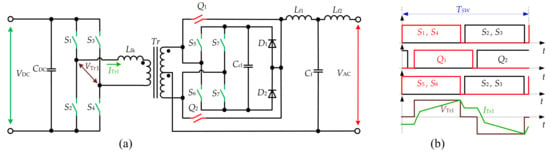
Two unipolar pulse-width modulation (PWM) based modulation methods for the FB isolated matrix inverter are reported in [6], both of these methods allow achieving the soft switching for the AC-side switches. In contrast, the DC side has only the zero voltage switching (ZVS) turn-on transient. The first method allows operating four switches at the AC side at line frequency, further reducing the remaining switching loss and improving the efficiency. The authors applied the hybrid structure of the switches at the AC side –four of them are IGBT with grid frequency switching and four MOSFET with high working frequency. This allows price reduction of the converter, which was the authors’ aim. The second modulation method is proposed for the full MOSFET bridge configuration. In this method, two of the switches working with the line frequency, two–as synchronous switches, and all the other are forming the output voltage. The authors verified the experimental 1.2-kW prototype with 400-V DC input voltage and 240-V AC RMS output using one to one isolation transformer. The peak efficiency of the system is 96% for the full silicon carbide (SiC) MOSFET design. In [12], the same group of authors presented applications for this converter in the high-frequency distributed power delivery system. This utilization allows elimination of the traditional low-frequency transformer and its replacement it with HFT. The potential target application is air and ground transportation and renewable energy systems.
In some studies, the leakage inductor energy is redirected to the additional auxiliary circuit, which allows the clamp of the voltage overshoot. In [7], the new modulation method based on the DC-side PSM is addressed for the FB inverter operation. For the minimization of voltage overshoot across AC-side switches, the clamping circuit with the rectifier bridge, capacitor and DC–DC converter is applied. The energy from the AC side is returned to the DC input and reused again in the converter. The topology is verified with 1 kW with 270 V of input and 100-V RMS at the output as UPS inverter. Other clamping circuit approaches were addressed in [8][9][10][13]. These papers present different types of regenerative flyback snubber. Since this snubber is technically a separate converter, in addition to voltage clamping, it can provide additional features for the topology: reduce the amount of the circulation current through the main switches, improve the soft-start procedure or improve the quality of the current in the case of non-unity power factor. The energy stored in the snubber capacitor can be utilized in two ways–being reused in the next switching cycle of the conversion, as proposed in [8][9] or transferred back to the DC side and reused again as shown in [13]. In addition, it is claimed to allow improving the efficiency of the converter in general. In [14], different snubbers for the minimization of the influence of high step-up transformer are analyzed for the case of the integration of low-voltage DC source to the grid. On the other hand, the utilization of the snubbers requires an additional transformer or two flyback transformers, switches, diodes, capacitors and additional control channels and isolated drivers. The utilization of this snubber can be more suitable for the high-power converter. For the lower-power converters, this solution can be less optimal, considering the price and overall complexity.
Many high-power converters commonly use bridge-type topologies due to the better utilization of the switches and lower stresses. The FB topologies can be extended to the three-phase grid system, as presented in [4][15][16][17]. In this case, at the AC side, an additional leg is supplied and the modulation method is extended for the three-phase system (Figure 2).
Figure 27. Three-phase FB configuration.
Three-phase FB configuration.1.1.2. Full Bridge Configuration with Three Legs at the DC Side
Full Bridge Configuration with Three Legs at the DC Side
In [18], the AC side PSM modulated PV microinverter is proposed (Figure 3). The topology utilizes three switching legs and a special high-frequency transformer. The additional bridge leg operates with a phase shift to the main bridge and allows generation of the two-step voltage waveforms, which are afterwards converted to the AC voltage. The two-step voltage allows reducing the ringing of the AC-side switches. The topology allows achieving the soft switching in all semiconductors at the AC side, while on the DC side, only two switches have hard transients. This solution is suggested to improve the efficiency of the system compared to the topology with the RCD snubber at the AC side. The peak efficiency reported is 95%.
1.1.3. Full Bridge Configuration with the Reconfigurable AC Side
Full Bridge Configuration with the Reconfigurable AC Side
The topology reported in [19][20] is proposed as a unidirectional inverter for the FC applications (Figure 4). It features two transformers and two bidirectional AC side bridges, which can be connected in series or in parallel, providing the universal output. The topology utilizes the sine PWM at the DC side, while half of the AC-side switches work with the grid frequency to minimize the switching losses in the converter. The design focuses on the universality of the output voltage and is suitable for both 230 V and 110 V and has a high step-up factor to achieve the connection 30–60-V fuel cell and is claimed to be optimal in terms of weight and cost. The authors achieved a peak efficiency of 92.5% for the proposed concept. The leakage inductances of the transformer are utilized for the soft switching in the semiconductors, but at the same time, the voltage overshoot appears across the AC-side switches. This suggests that the design and optimization of the transformer can be further considered to achieve better efficiency and reduce the stresses in the topology.
1.1.4. The Full Bridge Configuration with Push-Pull at the DC Side
The Full Bridge Configuration with Push-Pull at the DC Side
Figure 5 shows the topology reported in [21] as a unidirectional inverter for renewable energy sources. The topology has two switches at the DC side connected to a central-tapped transformer, forming the PP configuration. The AC side features the FB configuration. The multiple-carrier PWM is proposed for this topology. It was suggested that this technique allows reducing the complexity of the control algorithm for the inverter. The topology is suitable for low power applications; the simulation results of the 200-W prototype were shown for 48 VDC input voltage and 127-V RMS output voltage, using a transformer with a turns ratio of 1 to 4.2. An alternative configuration of a bidirectional converter based on the Cuk, SEPIC, Zeta converters is presented in [22] where the 400-W prototype of the SEPIC converter is demonstrated.
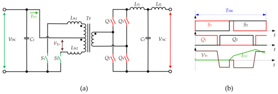
Figure 510.
FB configuration with push–pull (PP) at the DC side (a
) and modulation (b) in [21].
) in [78].In [23], the focus is on a multilevel PP inverter configuration. It utilizes the central tap transformer on both the DC and the AC side and includes an additional bidirectional switch at the AC side. The presence of the additional switch at the AC side and a special modulation strategy based on PSM allows avoiding the current interruption at the AC side, and as a result, voltage overshoots. The paper provides experimental verification on a 162-W prototype with 24-V input DC voltage and 100-V output AC voltage. In addition, the topology is suitable for bidirectional operation.
1.1.5. Half Bridge Configuration
Half Bridge Configuration
The topology in Figure 6 [24] is proposed as a unidirectional microinverter for PV applications. It features two transformer windings and two bidirectional switches at the AC side, which work at the line frequency. Thus, the total number of AC-side transistors is reduced by a factor of two when compared to the topology in Figure 1. The DC side, as described, could be configured as a FB, half bridge (HB) or push-pull (PP), which can allow reducing the total number of the semiconductors even further. Sine PWM is applied to the DC side semiconductors, realized by a comparison of two 180° phase-shifted sinewaves with a dual-sided ramp wave. At the AC side, the IGBT switches are utilized with line switching frequency to minimize the losses in the converter. The reported peak efficiency of the 250-W prototype is 94.5%. On the other hand, the ZVS for the DC-side switches has a limited range (occurs at peak power), and the AC-side switches have higher voltage stresses.
1.1.6. LL (dual inductor) HB Configuration
LL (dual inductor) HB Configuration
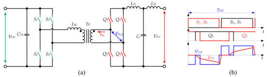
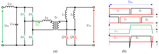
The dual inductor half-bridge (LL HB) converter type is a popular solution in the DC–DC converters due to the low current ripple. Figure 7 presents the bidirectional converter topology proposed for electric vehicle battery charging applications in [25][26]. The original paper describes it as “single-stage bidirectional converter for EV”; however, it will be referred here as LL HB due to the topology configuration. The converter features a full-bridge on the DC side with an additional filter inductor L
DC and LL-type HB at the AC side. The converter with the input of 120-V RMS AC is connected to a 220–336 VDC battery through a converter that has a high-frequency transformer with a turn ratio of 0.5. In the rectifier mode, the converter operates as a two-phase boost converter, while in the inverter mode, it acts similar to a FB converter with the current doubler rectifier the output voltage regulation is achieved by PSM. The converter features reduced current ripple due to the presence of two inductances at the AC side, allowing the ZCS to be achieved at the AC side, and ZVS turn-on at the DC side. Moreover, it can operate in four quadrants with active and reactive power regulation for both directions of the power flow. In the inverter mode, the PSM is implemented for the DC-side switches, while the AC-side switches are continuously on or off depending on the polarity of the grid voltage. Peak efficiency of 96.5% at full power is reported for the 1.5-kW prototype. At the same time, the topology requires an additional inductor, the voltage stress on the switches is increased, and it is estimated to have substantial energy circulation at partial load. The simulation results of the three-phase system shown in [27].
1.2. Non-Resonant Push-Pull Topologies
Non-Resonant Push-Pull Topologies
1.2.1. Push-Pull Configuration
Push-Pull Configuration
The topology in Figure 8a was introduced in [28] for the UPS. The topology utilizes the central tapped transformer and two bidirectional switches at the AC side, while the DC side has a FB inverter. In [29], the converter was controlled with sine PWM modulation at the DC side. In [30], an improved modulation method is introduced to handle the non-unity power factor without snubbers. A novel digital control using the bipolar double modulation wave was addressed in [12], which is shown in Figure 8b. The sinusoidal output voltage is formed by AC-side semiconductors using PSM. It allows achieving the ZVS turn-on on the DC side, and the ZVS turn-off at the AC side. The experimental verification of the topology was presented using an experimental 250-W prototype with and 46-V output voltage. In [31], the topology with four additional snubber capacitors for switches S1-S4 is presented. The aim is to achieve the ZVS and ZCS in all semiconductor devices using PSM. The experimental waveforms of the prototype with 24-V input voltage and transformer 1:2.74 are shown. Another version of the PSM is used in [32] to achieve the ZVS in the topology, which was confirmed with a 1-kW experimental setup. Reference [33] presents the unidirectional converter for PV application, which utilizes the additional two inductors at the AC side.
The three-phase system for the three-phase drive reported in [35] is shown in Figure 9. The topology has three parallel ports to support bidirectional operation with the source commutation method. The topology is also suitable for the UPS, PV and battery storage systems.
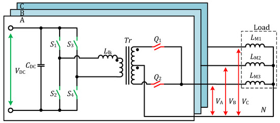
Figure 914. The three-phase PP configuration.
A novel ZVS approach for the flyback—PP inverter for low-power PV application is presented in [36]. The AC part of the topology is similar to that in Figure 9, while the input DC bridge is replaced by one switch, forming the flyback configuration. The soft-switching on the DC-side switch is achieved by additional circulating energy from the grid filter capacitor. To optimize this reactive current, the variable frequency control was proposed. Experimental results confirm the feasibility and show 94.5% peak efficiency of the system.
1.2.2. Push-Pull Configuration with voltage clamper
Push-Pull Configuration with voltage clamper
The topology of the bidirectional inverter presented in Figure 10 was introduced in [37] for the UPS system. The topology configuration consists of FB on the DC side, a central-tapped transformer with two bidirectional switches on the AC side and an additional clamping circuit. This active clamping circuit is proposed for the minimization of the voltage overshoots. It consists of four switches, which form the bridge, two diodes and clamp capacitor (the configuration without the capacitor is also possible [37]). The energy stored in the capacitor is transferred back to the DC source and reutilized. The SPWM is used to control the DC side, while AC-side switches are rectifying. The drawbacks could be attributed to a limited ZVS range, extra two diodes and a capacitor when compared to the FB solution without a snubber circuit.
Other approaches to control the configuration of the bridge clamp are reported in [38][39][40][41]. In [38][42], a detailed analysis of the operation of the bidirectional topology and clamping circuits is given. The experimental waveforms of the 500-W prototype with efficiency around 90% are provided, and the converter is proposed for renewable, naval and aerospace applications. In [40][42], the topology was proposed for the low-power audio amplifier. The operation principle of the uni- and bipolar PSM strategy is described and verified. In [39], an alternative bipolar PWM is proposed. It is suggested to allow achieving lower voltage distortion of the output compared to the unipolar PWM.
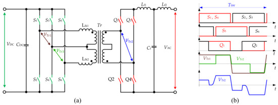
1.2.3. Push-Pull Configuration with the Current Clamping Switch
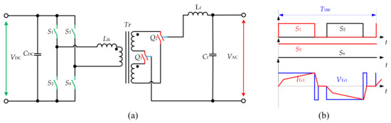
The topology presented in Figure 11 [43][44][45] uses a standard full-bridge at the DC side. However, the AC side is realized with a center-tapped transformer and three bidirectional switches. In the original paper, the AC side structure was described as “three bidirectional switching arms” and referred to as PP configuration with the current clamping switch in this review due to the topology configuration. The DC side FB converts the DC voltage to the HF AC square wave. On the AC side, the switching signals are obtained by comparing the modulating waveform with the sawtooth carrier waveform. The bidirectional switch Q3 connected to the center tap is turned on when both Q1 and Q2 are in the off-state to provide a freewheeling path for the output current. The additional overlap is added to realize the natural commutation of semiconductor devices and reduce overvoltage. The converter realizes ZVS and ZCS for the semiconductor switches and requires three bidirectional switches instead of four for the FB–FB topology. The bidirectional operation capability is reported, but not addressed.
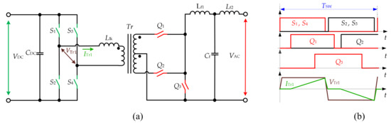
Figure 116.
PP configuration with the current clamping switch (a
) and modulation (b) in [44].
) in [121].Other versions of the topology for the bidirectional battery charger are reported in [46]. It utilizes three bidirectional switches with regenerative flyback clamp circuit at the AC side, while the DC side is FB. The presence of the clamping circuit allows the reduction of the voltage overshoot in AC and also helps to achieve the ZCS in the AC switches. The energy stored in the clamp capacitor is returned to the DC side and reused. The unipolar SPWM modulation strategy is used for both power transfer directions. The concept is verified with a 1.5-kW prototype with a 96% peak efficiency conversion from 300-V battery to the 120-V RMS grid.
1.3. Resonant Push-Pull Topologies
Resonant Push-Pull Topologies
1.3.1. Push-Pull Configuration with a Parallel Resonant Tank at the DC Side
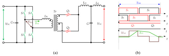
In [47], the sine AM modulation (SAM) was proposed as an alternative approach for the conventional PWM with varied duty cycles. The topology consists of the PP configuration at the AC side and the FB with the parallel resonant tank at the DC side (Figure 12). The resonant tank is connected between the middle point of the bridge legs and the middle point of the input voltage source. The bridge leg is operated with a varying duty cycle and a constant phase shift. The switching frequency of the converter is slightly higher than the resonant to extend the load independence and enable ZVS in the semiconductors.
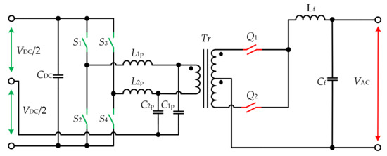
Figure 127. PP configuration with a parallel resonant tank at the DC side.
PP configuration with a parallel resonant tank at the DC side.The results are verified with a simulation model of a 2-kW converter. The converters with the parallel and with the series resonant tank were analyzed for the connection 450-V DC source with the utility grid. It is shown that the topology in Figure 17 has lower efficiency than the voltage source version on the topology with the series resonant tank, which will be described later.
The resonant inverter based on the topology from Figure 13 was introduced in [48][49] and described in more detail in [50]. It uses a resonant capacitor in series to the leakage inductance. The topology is proposed for the UPS application and features a lower output voltage ripple. It allows soft switching in the semiconductors using the SPWM modulation applied for FB thanks to the presence of the resonant tank at the DC side. The AC-side switches are forming, working at the grid AC waveforms.
- Mennicken, H. Stromrichtersystem Mit Wechselspannungs-Zwischenkreis Und Seine Anwendung in der Traktionstechnik. Ph.D. Thesis, RWTH Aachen University, Aachen, Germany, 1978. [Google Scholar]
- Kawabata, T.; Honjo, K.; Sashida, N.; Sanada, K.; Koyama, M. High frequency link DC/AC converter with PWM cycloconverter. In Proceedings of the Conference Record of the 1990 IEEE Industry Applications Society Annual Meeting, Seattle, WA, USA, 7–12 October 1990; Volume 2, pp. 1119–1124. [Google Scholar]
- Matsui, M.; Nagai, M.; Mochizuki, M.; Nabae, A. High-frequency link DC/AC converter with suppressed voltage clamp circuits-naturally commutated phase angle control with self turn-off devices. IEEE Trans. Ind. Appl. 1996, 32, 293–300. [Google Scholar] [CrossRef]
- Krishnaswami, H. Photovoltaic microinverter using single-stage isolated high-frequency link series resonant topology. In Proceedings of the 2011 IEEE Energy Conversion Congress and Exposition, Phoenix, AZ, USA, 17–22 September 2011; pp. 495–500. [Google Scholar]
- Surapaneni, R.K.; Yelaverthi, D.B.; Rathore, A.K. Cycloconverter-Based Double-Ended Microinverter Topologies for Solar Photovoltaic AC Module. IEEE J. Emerg. Sel. Top. Power Electron. 2016, 4, 1354–1361. [Google Scholar] [CrossRef]
- Mazumder, S.K.; Burra, R.K.; Huang, R.; Tahir, M.; Acharya, K. A Universal Grid-Connected Fuel-Cell Inverter for Residential Application. IEEE Trans. Ind. Electron. 2010, 57, 3431–3447. [Google Scholar] [CrossRef]
- Krein, P.; Balog, R.; Geng, X. High-Frequency Link Inverter for Fuel Cells Based on Multiple-Carrier PWM. IEEE Trans. Power Electron. 2004, 19, 1279–1288. [Google Scholar] [CrossRef]
- Iyer, K.; Mohan, N. Modulation and Commutation of a Single Stage Isolated Asymmetrical Multilevel Converter for Integration of Renewables and Battery Energy Storage System in Ships. IEEE Trans. Transp. Electrif. 2016, 2, 1. [Google Scholar] [CrossRef]
- Norrga, S. A soft-switched bi-directional isolated AC/DC converter for AC-fed railway propulsion applications. In Proceedings of the 2002 International Conference on Power Electronics, Machines and Drives, Sante Fe, NM, USA, 4–7 June 2002; pp. 433–438. [Google Scholar]
- Jauch, F.; Biela, J. Single-phase single-stage bidirectional isolated ZVS AC-DC converter with PFC. In Proceedings of the 2012 15th International Power Electronics and Motion Control Conference (EPE/PEMC), Novi Sad, Serbia, 4–6 September 2012. [Google Scholar]
- Basu, K.; Mohan, N. A High-Frequency Link Single-Stage PWM Inverter With Common-Mode Voltage Suppression and Source-Based Commutation of Leakage Energy. IEEE Trans. Power Electron. 2013, 29, 3907–3918. [Google Scholar] [CrossRef]
- Alluhaybi, K.; Batarseh, I.; Hu, H.; Chen, X. Comprehensive Review and Comparison of Single-Phase Grid-Tied Photovoltaic Microinverters. IEEE J. Emerg. Sel. Top. Power Electron. 2020, 8, 1310–1329. [Google Scholar] [CrossRef]
- Fornage, M.; Hassan-Ali, M.; Omar, T.H. Method and Apparatus for Providing Power Conversion Using an Interleaved Flyback Converter with Automatic Balancing. Patent EP2043246A2, 2007. Available online: https://patents.google.com/patent/EP2043246A2/ru (accessed on 9 May 2020).
- Harrison, M.J.; Zimmanck, D.R. Single-Phase Cycloconverter with Integrated Line-Cycle Energy Storage. Patent WO2015038995A1, 2014. Available online: https://patents.google.com/patent/WO2015038995A1/en?oq=WO2015038995A1 (accessed on 9 May 2020).
- Kimball, J.W.; Krein, P.T.; Benavides, N.D. Modular System for Unattended Energy Generation and Storage. Patent US8350411B2, 2006. Available online: https://patents.google.com/patent/US8350411B2/en (accessed on 9 May 2020).
- Kwon, O.; Kim, J.; Kwon, J.-M.; Kwon, B.-H. Bidirectional Grid-Connected Single-Power-Conversion Converter With Low-Input Battery Voltage. IEEE Trans. Ind. Electron. 2017, 65, 3136–3144. [Google Scholar] [CrossRef]
- Chen, W.W.; Zane, R.; Corradini, L. Isolated Bidirectional Grid-Tied Three-Phase AC–DC Power Conversion Using Series-Resonant Converter Modules and a Three-Phase Unfolder. IEEE Trans. Power Electron. 2017, 32, 9001–9012. [Google Scholar] [CrossRef]
- Diogo, A.C.P.B.V.; Luís, M.F.M.; Rui, M.E.A. Single-Phase Cycloconverter with Integrated Line-Cycle Energy Storage. Patent US9973107B2, 2015. Available online: https://patents.google.com/patent/US9973107B2/en (accessed on 9 May 2020).
- Guo, S.; Su, J.; Guo, L.; Chen, X. Phase-shifted modulation strategies for a single-stage isolated bi-directional power amplifier. In Proceedings of the 2016 IEEE 8th International Power Electronics and Motion Control Conference (IPEMC-ECCE Asia), Hefei, China, 22–26 May 2016; pp. 1206–1211. [Google Scholar]
- Norrga, S.; Meier, S.; Ostlund, S. A three-phase soft-switched isolated AC/DC converter without auxiliary circuit. IEEE Trans. Ind. Appl. 2004, 44, 836–844. [Google Scholar] [CrossRef]
- Vangen, K.; Melaa, T.; Bergsmark, S.; Nilsén, R. Efficient high-frequency soft-switched power converter with signal processor control. In Proceedings of the Thirteenth International Telecommunications Energy Conference—INTELEC 91, Kyoto, Japan, 5–8 November 1991; pp. 631–639. [Google Scholar]
- Aganza-Torres, A.; Cardenas, V. Analysis and modelling of HF-Link Cycloconverter based inverter for low-power renewable energy sources applications. In Proceedings of the 2011 8th International Conference on Electrical Engineering, Computing Science and Automatic Control, Merida City, Mexico, 26–28 October 2011; pp. 1–6. [Google Scholar]
- Kummari, N.; Chattopadhyay, S. Three-Legged High-Gain Phase-Modulated DC–AC Converter for Mitigation of Device Capacitance Induced Ringing Voltage. IEEE Trans. Power Electron. 2020, 35, 1306–1321. [Google Scholar] [CrossRef]
- Knabben, G.C.; Neumayr, D.; Kolar, J.W. Constant duty cycle sinusoidal output inverter with sine amplitude modulated high frequency link. In Proceedings of the 2018 IEEE Applied Power Electronics Conference and Exposition (APEC), San Antonio, TX, USA, 4–8 March 2018; pp. 2521–2529. [Google Scholar]
- Zhou, X.; Xu, J.; Zhong, S. Single-Stage Soft-Switching Low-Distortion Bipolar PWM Modulation High-Frequency-Link DC–AC Converter With Clamping Circuits. IEEE Trans. Ind. Electron. 2018, 65, 7719–7729. [Google Scholar] [CrossRef]
- Yamato, I.; Tokunaga, N.; Matsuda, Y.; Suzuki, Y.; Amaro, H. High frequency link DC-AC converter for UPS with a new voltage clamper. In Proceedings of the 21st Annual IEEE Conference on Power Electronics Specialists, San Antonio, TX, USA, 11–14 June 1990; pp. 749–756. [Google Scholar]
- Zhu, W.; Zhou, K.; Cheng, M. A Bidirectional High-Frequency-Link Single-phase Inverter: Modulation, Modeling, and Control. IEEE Trans. Power Electron. 2013, 29, 4049–4057. [Google Scholar] [CrossRef]
- Zhu, W.; Zhou, K.; Cheng, M.; Peng, F. A High-Frequency-Link Single-Phase PWM Rectifier. IEEE Trans. Ind. Electron. 2014, 62, 289–298. [Google Scholar] [CrossRef]
- Nayak, P.; Rajashekara, K. Single-Stage Bi-Directional Matrix Converter with Regenerative Flyback Clamp Circuit for EV Battery Charging. In Proceedings of the 2019 IEEE Transportation Electrification Conference and Expo (ITEC), Detroit, MI, USA, 19–21 June 2019; pp. 1–6. [Google Scholar]
- Trubitsyn, A.; Pierquet, B.J.; Hayman, A.K.; Gamache, G.E.; Sullivan, C.R.; Perreault, D.J. High-efficiency inverter for photovoltaic applications. In Proceedings of the 2010 IEEE Energy Conversion Congress and Exposition, Atlanta, GA, USA, 12–16 September 2010; pp. 2803–2810. [Google Scholar]
- Liu, Y.; He, J.; Ge, B.; Li, X.; Xue, Y.; Blaabjerg, F. A Simple Space Vector Modulation of High-Frequency AC Linked Three-Phase-to-Single-Phase/DC Converter. IEEE Access 2020, 8, 59278–59289. [Google Scholar] [CrossRef]
- Wang, S.; Gao, H.; Afsharian, J.; Xu, D. High Frequency Bidirectional Isolated Matrix Converter for AC-Motor Drives with Model Predictive Control. In Proceedings of the 2019 IEEE Energy Conversion Congress and Exposition (ECCE), Baltimore, MD, USA, 29 September–3 October 2019; pp. 5597–5602. [Google Scholar]
- Samares, K. High Permittivity Gate Dielectric Materials, Chapter 2: MOSFET: Basics, Characteristics, and Characterization; Springer: Berlin/Heidelberg, Germany, 2013; ISBN 978-3-642-36534-8. [Google Scholar]
- Kumar Khanna, V. Insulated Gate Bipolar Transistor IGBT Theory and Design; Wiley: Hoboken, NJ, USA, 2003; pp. 35–100. ISBN 780471238454. [Google Scholar]
- Erickson, R.W.; Maksimović, D. Fundamentals of Power Electronics, 2nd ed.; Kluwer Academic: Norwell, MA, USA, 2001; pp. 88–92. [Google Scholar]
- Takei, M.; Harada, Y.; Ueno, K. 600 V-IGBT with reverse blocking capability. In Proceedings of the Power Semiconductor Devices and ICs, 2001. ISPSD ’01. Proceedings of the 13th International Symposium on, Osaka, Japan, 7 June 2001; pp. 413–416. [Google Scholar]
- Klumpner, C.; Blaabjerg, F. Using reverse-blocking IGBTs in power converters for adjustable-speed drives. IEEE Trans. Ind. Appl. 2006, 42, 807–816. [Google Scholar] [CrossRef]
- Hofmann, D. High efficient power modules for dispersed generation units using reverse blocking IGBTS. In Proceedings of the 2014 IEEE 5th International Symposium on Power Electronics for Distributed Generation Systems (PEDG), Galway, Ireland, 24–27 June 2014; pp. 1–5. [Google Scholar]
- Zinchenko, D.; Korkh, O.; Blinov, A.; Waind, P.; Vinnikov, D. Characterisation of 1200 V Reverse-Blocking IGBTs for Naturally Commutated HF-Link Inverter. In Proceedings of the 2019 IEEE 2nd Ukraine Conference on Electrical and Computer Engineering (UKRCON), Lviv, Ukraine, 2–6 July 2019; pp. 382–387. [Google Scholar]
- Hosseini, S.; Sabahi, M.; Goharrizi, A. Multi-function zero-voltage and zero-current switching phase shift modulation converter using a cycloconverter with bi-directional switches. IET Power Electron. 2008, 1, 275–286. [Google Scholar] [CrossRef]
- Prasanna, U.R.; Singh, A.K.; Rajashekara, K. Novel Bidirectional Single-phase Single-Stage Isolated AC–DC Converter With PFC for Charging of Electric Vehicles. IEEE Trans. Transp. Electrif. 2017, 3, 536–544. [Google Scholar] [CrossRef]
- Singh, A.K.; Prasanna, U.R.; Rathore, V.; Rajashekara, K.; Ben-Brahim, L.; Gastli, A. A Soft Switching Single Stage Isolated Three Phase Bidirectional PFC Converter for Electric Vehicles charging. In Proceedings of the 2019 North American Power Symposium (NAPS), Wichita, KS, USA, 13–15 October 2019; pp. 1–6. [Google Scholar]
- Tazume, K.; Aoki, T.; Yamashita, T. Novel method for controlling a high-frequency link inverter using cycloconverter techniques. In Proceedings of the PESC 98 Record. 29th Annual IEEE Power Electronics Specialists Conference (Cat. No.98CH36196), Fukuoka, Japan, 22–22 May 1998; Volume 1, pp. 497–502. [Google Scholar]
- Jauch, F.; Biela, J. Combined Phase Shift and Frequency Modulation of a Dual Active Bridge AC-DC Converter with PFC. IEEE Trans. Power Electron. 2016, 31, 1. [Google Scholar] [CrossRef]
- Das, D.; Basu, K. A Soft-switched isolated Single Stage Bidirectional Three phase AC-DC Converter. In Proceedings of the 2019 IEEE Energy Conversion Congress and Exposition (ECCE), Baltimore, MD, USA, 29 September–3 October 2019; pp. 596–601. [Google Scholar]
- Chen, T.; Yu, R.; Huang, Q.; Huang, A.Q. A single-stage bidirectional dual-active-bridge AC-DC converter based on enhancement mode GaN power transistor. In Proceedings of the 2018 IEEE Applied Power Electronics Conference and Exposition (APEC), San Antonio, TX, USA, 4–8 March 2018; pp. 723–728. [Google Scholar]
- Yamato, I.; Tokunaga, N.; Matsuda, Y.; Amano, H.; Suzuki, Y. New conversion system for UPS using high frequency link. In Proceedings of the PESC ’88 Record., 19th Annual IEEE Power Electronics Specialists Conference, Kyoto, Japan, 11–14 April 1988; Volume 2, pp. 658–663. [Google Scholar]
- Kan, J.; Xie, S.; Wu, Y.; Tang, Y.; Yao, Z.; Chen, R. High-Frequency-Link Inverter Using Combined Synchronous Rectifiers. IEEE Trans. Ind. Electron. 2014, 61, 6769–6777. [Google Scholar] [CrossRef]
- Bhattacharjee, A.K.; Batarseh, I. Sinusoidally Modulated AC-Link Microinverter Based on Dual-Active-Bridge Topology. IEEE Trans. Ind. Appl. 2020, 56, 422–435. [Google Scholar] [CrossRef]
- Das, D.; Weise, N.; Basu, K.; Baranwal, R.; Mohan, N. A Bidirectional Soft-Switched DAB-Based Single-Stage Three-Phase AC–DC Converter for V2G Application. IEEE Trans. Transp. Electrif. 2018, 5, 186–199. [Google Scholar] [CrossRef]
- Koushki, B.; Jain, P.; Bakhshai, A. Topology and controller of an isolated bi-directional AC-DC converter for electric vehicle. In Proceedings of the 2016 IEEE Energy Conversion Congress and Exposition (ECCE), Milwaukee, WI, USA, 18–22 September 2016; pp. 1–8. [Google Scholar]
- Wang, M.; Huang, A.Q.; Yu, W.; Huang, A.Q. High-frequency AC distributed power delivery system. In Proceedings of the 2016 IEEE Applied Power Electronics Conference and Exposition (APEC), Long Beach, CA, USA, 20–24 March 2016; pp. 3648–3654. [Google Scholar]
- Nayak, P.; Pramanick, S.; Rajashekara, K. Isolated Single Stage AC-DC Converter Topologies with Regenerative Snubber Circuit for EV Application. In Proceedings of the IECON 2018—44th Annual Conference of the IEEE Industrial Electronics Society, Washington, DC, USA, 21–23 October 2018; pp. 1285–1290. [Google Scholar]
- Korkh, O.; Blinov, A.; Vinnikov, D. Analysis of Oscillation Suppression Methods in the AC–AC Stage of High Frequency Link Converters. In Proceedings of the 2019 IEEE 60th International Scientific Conference on Power and Electrical Engineering of Riga Technical University (RTUCON), Riga, Latvia, 7–9 October 2019; pp. 1–5. [Google Scholar]
- Inagaki, K.; Okuma, S. High frequency link DC/AC converters using three phase output PWM cycloconverters for uninterruptible power supplies. In Proceedings of the Thirteenth International Telecommunications Energy Conference—INTELEC 91, Kyoto, Japan, 5–8 November 1991; pp. 580–586. [Google Scholar]
- Cardoso, R.; Barbi, I. New bi-directional DC-AC converters with high frequency isolation. In Proceedings of the International Symposium on Signals, Circuits and Systems, Iasi, Romania, 14–15 July 2005; Volume 2, pp. 593–596. [Google Scholar]
- Beristain, J.; Bordonau, J.; Raventos, O.; Rocabert, J.; Busquets-Monge, S.; Mata, M. A New Single-Phase HF-Link Multilevel Inverter. In Proceedings of the 2005 IEEE 36th Power Electronics Specialists Conference, Recife, Brazil, 16 June 2005; pp. 237–243. [Google Scholar]
- Singh, A.K.; Prasanna, R.; Rajashekara, K. Modelling and Control of Novel Bidirectional Single-Phase Single-Stage Isolated AC-DC Converter with PFC for Charging of Electric Vehicles. In Proceedings of the 2018 IEEE International Conference on Electro/Information Technology (EIT), Rochester, MI, USA, 3–5 May 2018; pp. 661–666. [Google Scholar]
- Mazumder, S.K.; Rathore, A.K. Primary-Side-Converter-Assisted Soft-Switching Scheme for an AC/AC Converter in a Cycloconverter-Type High-Frequency-Link Inverter. IEEE Trans. Ind. Electron. 2010, 58, 4161–4166. [Google Scholar] [CrossRef]
- De Souza, K.; De Castro, M.; Antunes, F. A DC/AC converter for single-phase grid-connected photovoltaic systems. In Proceedings of the IEEE 2002 28th Annual Conference of the Industrial Electronics Society. IECON 02, Sevilla, Spain, 5–8 November 2002; Volume 4, pp. 3268–3273. [Google Scholar]
- Jingang, L.; Qingyuan, M.; Shaocheng, D. Research on a novel modulation technology for high-frequency link inverter. In Proceedings of the 2012 7th IEEE Conference on Industrial Electronics and Applications (ICIEA), Singapore, 18–20 July 2012; pp. 624–627. [Google Scholar]
- Sukesh, N.; Pahlevaninezhad, M.; Jain, P.K. Analysis and Implementation of a Single-Stage Flyback PV Microinverter With Soft Switching. IEEE Trans. Ind. Electron. 2013, 61, 1819–1833. [Google Scholar] [CrossRef]
- Guo, S.; Su, J.; Chen, X.; Yu, X. High-efficiency full-range soft-switching full-bridge high-frequency-link inverter. Electron. Lett. 2016, 52, 1944–1946. [Google Scholar] [CrossRef]
- Nge, C.L.; Chin, V.J. Unipolar SPWM HF link soft switching DC/AC converter. In Proceedings of the PECon 2004. Proceedings. National Power and Energy Conference, Kuala Lumpur, Malaysia, 29–30 November 2004; pp. 116–120. [Google Scholar]
- Nge, C.-L.; Salam, Z. Application of Natural Commutation Technique to Center-Tapped HF Link Inverter. In Proceedings of the 2005 International Conference on Power Electronics and Drives Systems, Kuala Lumpur, Malaysia, 28 November–1 December 2005; pp. 90–94. [Google Scholar]
- Nge, C.; Salam, Z. Modified natural commutated switching technique for HF link inverter. In Proceedings of the 2005 European Conference on Power Electronics and Applications, Dresden, Germany, 11–14 September 2005; p. 7. [Google Scholar]
- Bhat, A.K.S.; Dewan, S.D. Resonant inverters for photovoltaic array to utility interface. IEEE Trans. Aerosp. Electron. Syst. 1988, 24, 377–386. [Google Scholar] [CrossRef]
- Chung, Y.-H.; Shin, B.-S.; Cho, G.-H. Bilateral series resonant inverter for high frequency link UPS. In Proceedings of the 20th Annual IEEE Power Electronics Specialists Conference, Milwaukee, WI, USA, 26–29 June 1989; Volume 1, pp. 83–90. [Google Scholar]
- Chung, Y.; Shin, B.; Cho, G. Bilateral series resonant inverter for high frequency link UPS. IEE Proc. B Electr. Power Appl. 1991, 138, 159. [Google Scholar] [CrossRef]