The discovery of the extremely shallow amorphous boron-crystalline silicon heterojunction occurred during the development of highly sensitive, hard and robust detectors for low-penetration-depth ionizing radiation, such as ultraviolet photons and low-energy electrons (below 1 keV). For many years it was believed that the junction created by the chemical vapor deposition of amorphous boron on n-type crystalline silicon was a shallow p-n junction, although experimental results could not provide evidence for such a conclusion. Only recently, quantum-mechanics based modelling revealed the unique nature and the formation mechanism of this new junction. Here, the entry reviews the initiation and the history of understanding the a-B/c-Si interface (henceforth called the “boron-silicon junction”).
- Boron-Silicon Junctions
1. Introduction: Initiation and History of Boron-Silicon Junctions and Importance of Si-Based Junctions/Diodes in Microelectronics
The first report about an ultra-shallow rectifying junction (diode) created by a pure boron atmospheric/low-pressure chemical vapor deposition (AP/LPCVD) on crystalline n-type silicon surface was published in 2006 [1]. Initially, the application which led to the development of this novel rectifying junction was: a linear and high Q-factor varactor diode designed for the capacitance tuning of frequency in RF circuits[2][3]. The demonstrated good performance in the varactor application did not attract the expected attention. Fortunately, in 2006 it became clear that a different field of applications would benefit even more from the excellent electrical properties of this extremely shallow junction. This junction would prove useful as an accurate, stable and reliable detector for low-penetration depth radiation such as UV light and low-energy electrons, which are applied in UV optical lithography and scanning electron microscopes.
Since 2006 a significant amount of research has been completed in the following directions: (1) optimization of the critical junction creation process, i.e., the chemical vapor deposition (CVD) of amorphous boron on n-type crystalline silicon (in a method called the “PureB” process); (2) device characterization and design optimization for a variety of applications; and (3) rendering the PureB process CMOS-compatible. Initially it was believed that the excellent electrical properties of the junction—especially the very low saturation currents which are typical for deep p-n junctions—were defined by the p+ delta-doping of the n-type substrate which simultaneously occurs during the boron CVD process[1]. It was assumed that the saturation current was mainly dominated by the hole injection from the p+ region into the n-substrate, as governed by the Gummel Number (GE) of this region. The high level of electron injection typically dominating the current in the Schottky diode counterpart was suppressed, although the actual p+ region was only a few nanometers thin[4]. However, it was difficult to explain the very high effective GE, keeping in mind the limited solubility of boron in silicon in the applied CVD temperature range from 500–700 °C[5]. Electrical measurements, as presented in[6], showed injection currents as low as a few 10−20 A/ μ m2, which was comparable to those achieved in deep, heavily doped junctions. This corresponded with a GE in the order of 1014–1015 atm/cm2, which was orders of magnitudes higher than what would be expected from nm-shallow junctions formed by bulk-doping the silicon. In the 700 °C PureB process the actual doping of the Si-substrate contributed to GE by roughly 1012 atm/cm2, as documented in[4]. In diodes that were formed solely by such a doping of the Si-substrate, the total current would approach Schottky diode-like values.
The idea of the delta-doped p+ layer playing any significant role in the junction formation was completely abandoned when it was demonstrated that similar excellent electrical properties could be achieved by boron CVD on n-type crystalline silicon substrates at temperatures as low as 400 °C, at which no doping of boron in silicon is expected[7].
Later on, in order to overcome the inconsistencies in the above-mentioned concept for the junction formation mechanism, it was suggested that the thickness of the amorphous boron layer was directly responsible for the junction behavior[1][4]. The bulk properties of the amorphous boron layer that could lead to the suppression of the electron injection included either: (i) a very short electron diffusion length and low electron mobility, which could cause quenching of the electron transport[4], or (ii) a wider bandgap than that of the Si, as proposed and supported by simulations in [8]. However, experimental results showed that even for a 1-second (s) boron deposition, where not even a monolayer of boron could be deposited, the junctions were reported to contain an equally high hole injection for both 700 °C and 500 °C depositions [6]. A closer look at the dependency between the thickness of the boron layer and the GE showed that after creating a very thin boron layer with a full coverage of the silicon substrate surface, the injection current stopped decreasing. This observation contradicted to the previous conclusion about the GE-boron thickness relation, and raised serious doubt about the dominant role of bulk amorphous boron for junction creation [6][8].
Thus, when the delta-doped p+ layer and the as-deposited boron layer thickness could no longer be considered dominant factors in the junction creation, what remained was the search for an answer in the physics behind the boron-silicon interface. In[6] the following proposition was made: “based on experimental evidence, the effectively high Gummel Number of the p+ region, which provides low saturation currents despite the shallowness of the junctions, was related to the formation of a virtually complete surface coverage of acceptor states as an interface property of boron on Si.” In a later publication[9] this idea was further developed: “the results can be explained with a simple model assuming a monolayer of acceptor states at the interface that fills with electrons to give a monolayer of fixed negative charge. Furthermore, it can be assumed that the high resistivity of the very thin PureB layer acts as a semi-insulating layer allowing an inversion layer of holes to be built up. (…) The monolayer of n-charge represents a very high electric field that binds the holes to the interface and limits their mobility, similar to the way a vertical electrical field attenuates the inversion layer mobility in MOS devices”.
However, this explanation of the junction formation had two major weaknesses:
-
There was no explanation as to where the “monolayer of acceptor states” providing “a monolayer of fixed negative charge” originates from;
-
It was not explained what made the charge “fixed”.
Despite the fact that the junction formation was most probably correctly allocated, the failure to explain its mechanism led to a “dose of despair”. In[5] we read: “However, even if the chemical bonding structure of the interface was well known, translating it into an electrical structure is no straightforward task as can be appreciated evaluating the enormous number of studies devoted to understanding the metal-semiconductor interfaces of Schottky diodes”.
Then, in 2017 a completely new concept regarding the junction formation with the PureB process was introduced[10]. It was proposed that this junction should not be considered a p-n type, and it should also not be assigned to any existing types of heterojunctions. That would clarify why the existing “instrumentarium” in semiconductor physics used to explain and predict the properties of known rectifying junctions could not be used successfully here. Instead, a deeper dive into solid-state physics and material science was proposed using a more powerful ”scientific weapon“—the theory of quantum mechanics. An analysis of the junction formation was reported in[10], which concluded that the chemical interaction between the surface atoms of crystalline silicon and the first atomic layer of the as-deposited amorphous boron was the dominant factor leading to the formation of a depletion zone in the crystalline silicon originating from the surface. A first-principles quantum mechanics molecular dynamics simulation showed a very strong electric field across the a-B/c-Si interface systems where the charge transfer occurred mainly from the interface Si atoms to the neighboring B atoms. This electric field appeared to be responsible for the creation of a depletion zone in the n-silicon, resulting in a rectifying junction formation. A more detailed introduction of this hypothesis is provided in Section 3. Before that, in Section 2, information is provided on the PureB process and the most attractive electrical and optical characteristics of the boron-silicon junction as a radiation detector.
2. The PureB Process and Characterization of the Boron-Silicon Junction as a Radiation Detector
2.1. The PureB Process and Temperature Effects
Amorphous pure boron (a-B) thin films can be deposited on crystalline Si substrates in ultra clean chambers with high purity gasses, by using chemical vapor deposition tools (e.g., cold-wall reactors or hot-wall furnaces) and physical vapor deposition techniques like: molecular beam epitaxy [12][11]] and sputtering [13].
Chemical vapor deposition (CVD) of the precursor molecule diborane (B2H6) is mostly employed to obtain high-quality ultra-thin (2–10 nm) a-B films. The CVD tools operate in a range of 400–800 °C, with pressure ranging from tens of Torr to atmospheric pressure (760 Torr). For CVD at temperatures higher than 400 °C, the diborane molecules decompose at the surface of the substrate into gas-phase boron hydrates. The most common resulting species is BH3 [14].
At the beginning of the deposition, the Si surface atoms have exposed dangling bonds to which the BH3 molecules react, creating a Si-B bond and the release of hydrogen. If the Si dangling bonds are passivated with H atoms, the latter must be desorbed before any Si-B bonds can be formed. In fact, it has been observed that the presence of H2 gas (generally used as a carrier and diluting gas) in the reactor reduces the a-B deposition rate[15]. When the coverage of the surface Si atoms by the BHx species is accomplished, the BH3 molecules react with the exposed B dangling bonds, which then generates B-B bonds (along with H/H2 release). The growth of the a-B film advances according to the adsorption-reaction mechanisms presented in[16].
Upon adsorption, the BH3 molecules diffuse along the surface before forming a stable bond. At temperatures between 400–600 °C, their surface migration is limited and the a-B grows into islands with the surface reactive sites[16][17][18]. The diffusion is strongly temperature-dependent. Figure 1 illustrates a schematic cross-section of the layer stack of the B-Si junction and the corresponding High-Resolution Tunneling Electron Microscope (HRTEM) images at deposition temperatures of 400 °C and 700 °C [10]. The HRTEM images confirm the lack of boron-silicide (BxSiy) layer for the samples obtained using the low temperature process (400 °C, Figure 1c), while for the samples prepared at the high temperature (700 °C, Figure 1d) a 1–2 nm-thick boron-silicide (BxSiy) can be observed. It was also reported that the silicide forms a uniform layer at deposition temperatures higher than 750 °C[15]. For deposition at ∼500 °C and below, the a-B contains significant portions of hydrogen, due to incomplete precursor dissociation, which eventually coalesce into a more rough film [16][17]. When deposition temperatures are higher than 700 °C, the surface diffusivity of the adsorbed precursors is enhanced allowing a smooth, continuous film to be deposited of minimal thickness (a few nm) [16].
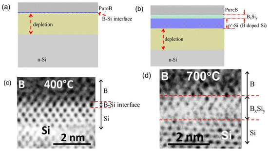
Figure 1. Schematic illustrations and High-Resolution Tunneling Electron Microscope (HRTEM) images of the cross-section of the layer stack: (a) schematic illustration of the cross-section of the B-Si junction processed at 400 °C; (b) Schematic illustration of the cross-section of the B-Si junction processed at 700 °C; (c) HRTEM image of the cross-section of the B-Si junction processed at 400 °C; (d) HRTEM image of the cross-section of the B-Si junction processed at 700 °C [10].
The diffusion of B atoms in bulk Si during the CVD of amorphous B becomes significant at temperatures above 750 °C. The experiments also showed that the diffusion rate of a-B at 600 °C is the same for both Si{0 0 1} and Si{1 1 1} surfaces, while at 800 °C, B atoms diffuse faster into the Si{0 0 1} subsurface [17].
2.2. Characterization of the Boron-Silicon Junction as a Radiation Detector
In the Introduction we revealed the main application driving the development of the PureB process: the detection of low-penetration depth radiation such as UV photons and low-energy electrons. Here we shall present the most attractive characteristics of the boron-silicon junction, in its application as a photodetector (photodiode). For this purpose we shall use as a reference the characteristics of an ideal photodetector, as presented in Table 1 and Figure 2 [19]. Figure 2 shows the vertical cross section of a silicon p-n junction photodetector and its electric circuit equivalent. Table 1 presents the parameter values of an ideal silicon photodiode, which provide the best performance with respect to: responsivity, resolution, speed and stability.
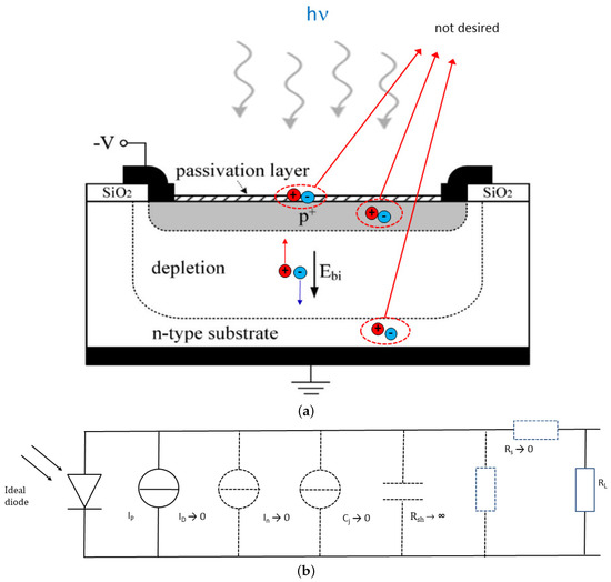
Figure 2. Vertical cross section (a), and electrical equivalent circuit (b) of a silicon p-n junction photodetector, where ID is the dark current, Ip is the photogenerated current, In is the shot noise associated with the dark current, Cj is the junction capacitance, Rsh is the shunt resistance, Rs is the series resistance and RL is the load resistance [19].
Table 1. Main characteristics and related parameters of an ideal silicon-based photodetector.
| Main Characteristics | Related Diode Parameters | Ideal Parameter Values |
|---|---|---|
| Responsivity | Passivation layer thickness | 0 |
| Depletion depth | 0 | |
| Depletion width | Optimized by the photon attenuation length | |
| Resolution | Dark current | 0 |
| Shunt resistance | ∞ | |
| Stability | Passivation Layer | Oxide-free, high-conductivity, protective |
| Operational speed | Series resistance | 0 |
| Junction capacitance | 0 |
2.2.1. Responsivity
The structure of the boron-silicon junction satisfies in an excellent way the three parameters affecting the responsivity: passivation layer thickness, depletion depth and width (see Table 1). The junction can be essentially created by a single layer of boron atoms deposited on the n-type silicon substrate, in such a way that chemical bonds are formed between the boron atoms and the surface silicon atoms.
For reliable protection of the underlying silicon from oxidation and potentially detrimental environment conditions, a few extra boron layers with a total thickness of a few nanometers are deposited in practice. The depletion region, where the photogenerated electron-hole pairs can be separated and collected, starts from the very first atomic layer of the underlying n-type silicon substrate. The lost radiation absorbed in the passivation layer is minimal due to its thinness. Figure 3 shows the measured spectral responsivity of a boron-silicon junction with a ∼5 nm amorphous boron protection layer in the extreme ultra violet (EUV) spectral range, compared with the theoretically attainable values for an ideal Si-based photodetector and a commercial n+p photodiode (SXUV from ODC) [19][20]. The measured responsivity above the silicon edge (12.4 nm) is 0.265 A/W, which is very close to that of an ideal lossless system (0.27 A/W), indicating 100% internal quantum efficiency. The slight drop in responsivity at wavelengths shorter than the silicon edge can be assigned to a very thin silicon absorbing layer above the depletion zone. However, most probably another phenomenon is playing a dominant role here: after the silicon edge, the penetration depth of the photons decreases significantly leading to the absorption of more photons close to the detector surface. The kinetic energy of the freed electrons is high enough to allow them to overcome the internal electric field and to move in an arbitrary direction, with some being lost due to recombination with the holes, while others may even escape from the surface of the detector as secondary electrons.
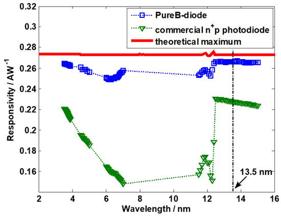
Figure 3. Measured spectral responsivity (squares) of boron-silicon photodiode in the extreme ultra violet (EUV) spectral range, compared with a commercial n+p photodiode and the theoretically attainable values for an ideal Si-based photodetector [20].
Figure 4 shows the measured spectral responsivity of a boron-silicon photodiode in the deep ultra violet (DUV) and vacuum ultra violet (VUV) spectral ranges[19]. As indicated in the figure, based on the measured responsivity at a 193 nm wavelength (0.0997 A/W) and the theoretical value (0.215 A/W), the quantum efficiency is: QE=0.0997/0.215≈0.46
Considering the nearly 100% quantum efficiency measured at a 13.5 nm wavelength (Figure 4), the loss due to the photon-generated electron-hole pairs recombining in the diode depletion region can be regarded as negligible. The main reason for the quantum efficiency drop in the VUV/DUV spectral range, besides the reflection-induced photon loss on the diode surface, is the extremely low penetration depth of the photons in the boron and silicon: only a few nanometers [21]. Because of this, even a 2-nm-thick boron layer will absorb a substantial part of the incident radiation.
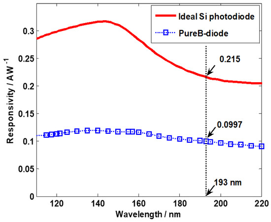
Figure 4. Measured responsivity of a boron-silicon photodiode with ∼2 nm boron layer, in the deep ultra violet (DUV)/vacuum ultra violet (VUV) spectral ranges, compared with the theoretically attainable values for an ideal Si-based photodetector [19].
2.2.2. Resolution
For achieving a very high resolution it is very important the interface between the silicon substrate and the passivation layer on top of it to be defect free. This is achieved by the PureB CVD process, during which the boron atoms form strong chemical bonds with the surface silicon atoms. The number of silicon dangling bonds (acting as recombination centers is extremely small. This results in an excellent I-V characteristic typical for a high-quality deep p-n junction, with a very low reverse-bias (dark) current and an ideality factor very close to 1 (Figure 5) [22], despite the fact the depletion region starts literally from the boron-silicon interface. A low dark current means a very low shot noise associated with it. The low value of the dark current maintained at high reverse-bias voltage is an evidence for a very high shunt resistance Rsh.
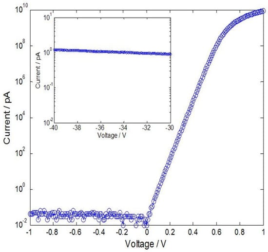
Figure 5. I-V characteristic of a boron-silicon diode with active area 300 × 300 μm2. The inset shows a dark current of 1 pA with a reverse bias up to −40V, corresponding to current density: ∼11 pA per square micrometer)[22].
2.2.3. Stability
The strong chemical bonds formed between the silicon and the boron atoms provide an excellent radiation shield, as they cannot be destroyed by UV photons or low-energy electrons. Experiments with extensive exposure up to 220 kJ/cm2 of a boron-silicon photodiode at 13.5 nm radiation could not reveal a measurable degradation of the responsivity[23]. A very small amount of responsivity degradation was observed in the VUV spectrum. Figure 6 shows the responsivity degradation of three boron-silicon junctions exposed to 121 nm radiation (radiation around 120 nm wavelength is considered the most challenging in the VUV spectrum) [19]. The difference between the three samples is the oxygen content on the surface, expressed as a thickness in nanometers. In this experiment high exposure levels are not necessary, as any available drop in responsivity is evident almost immediately at the start of the VUV exposure, subsequently settling to its lower level. The presence of oxygen is assigned to local oxidation of silicon through pin holes in the thin boron layer which only partially covers silicon. With VUV exposure the oxidized silicon surface is positively charged due to the secondary electron emission, temporarily reducing the responsivity. As can be seen in Figure 6, with 1 nm oxide the degradation is extremely small—within the margin of uncertainty of the measurement equipment. It is important to mention that this kind of degradation is recoverable with time as the positive charge dissipates very slowly.
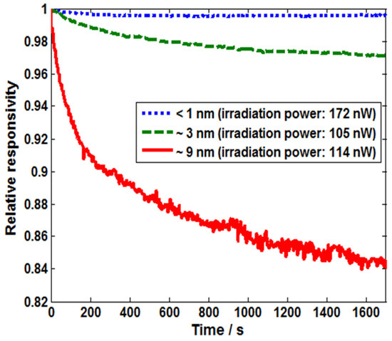
Figure 6. Responsivity degradation of 3 boron-silicon photodiodes with varying parasitic oxide content on the surface, at a 121-nm wavelength. The oxide content was measured by ellipsometry and is expressed as a thickness in nanometers[19].
Another factor influencing the photodiode stability is the working environment. In this aspect, the boron-silicon junction demonstrates very high robustness to harsh working conditions. Boron itself is a very stable material at room temperature. Furthermore, a nanometer-thin amorphous boron layer, when completely covering the underlying silicon, acts as an excellent barrier protecting the silicon substrate from detrimental environmental elements such as hydrogen radicals and oxygen plasma, used for surface cleaning purposes. Extensive exposure to such elements has not resulted in noticeable deterioration of the electrical or optical characteristics of the boron-silicon photodiode [23].
2.2.4. Operational Speed
For a fast reaction to pulsed radiation, the photogenerated charge must be removed quickly from the depletion region of the photodetector and delivered to the interface electronics. For this purpose the time constant of the detector—defined by the junction capacitance Cj and the series resistance Rs—must be small (Figure 2b). The value of the series resistance is dominated by the sheet resistance of the surface of the detector. This is because after separation, the photogenerated charge must reach the top ring electrode (Figure 2a) by moving along the surface of the detector. However, due to the high resistivity of the very thin boron layer and the fact that the depletion region starts from the silicon surface, the sheet resistance is very high. This makes the boron-silicon photodiode extremely slow. Furthermore, unlike a typical p-n junction detector—where the time constant can be decreased by reducing Cj with the application of a higher reverse-bias voltage, the same approach does not work well with the boron-silicon detector. Just the opposite, the time constant of the boron-silicon detector increases with a higher reverse-bias voltage despite the reduction in the junction capacitance. This is because apparently the series resistance increases faster than the decrease in the capacitance[24].
A solution to this problem is to trade some responsivity for the benefit of the time constant. For example, deploying a metal Al grid on top of the boron layer, which covers just 1% of the surface, leads to a dramatic reduction in the sheet resistance and the time constant, respectively [19].
References
- Sarubbi, F.; Nanver, L.K.; Scholtes, T.L. CVD Delta-Doped Boron Surface Layers for Ultra-Shallow Junction Formation. ECS Trans. 2006, 3, 35–44.
- Nanver, L.K.; Sarubbi, F.; Gonda, V.; Popadic, M.; Scholtes, T.L.; de Boer, W.; Buisman, K. Extremely ultrashallow junctions for a high-linearity silicon-on-glass RF varactor-diode technology. Extended Abstracts. In Proceedings of the 2008 8th International Workshop on Junction Technology (IWJT ‘08), Shanghai, China, 15–16 May 2008.
- Sarubbi, F. Characterization of Pure Boron Depositions Integrated in Silicon Diodes for Nanometer-Deep Junction Applications. Ph.D. Thesis, TU Delft Repository, Delft, The Netherlands, 2010.
- Sarubbi, F.; Nanver, L.K.; Scholters, L.M. High Effective Gummel Number of CVD Boron Layers in Ultrashallow p+n Diode Configurations. IEEE Trans. Electron. Devices 2010, 57, 1269–1278.
- Nanver, L.K.; Qi, L.; Mohammadi, V.; Mok, K.R.M.; de Boer, W.B.; Golshani, N.; Sammak, A.; Scholtes, T.L.M.; Gottwald, A.; Kroth, U.; et al. Robust UV/VUV/EUV PureB Photodiode Detector Technology With High CMOS Compatibility. IEEE J. Sel. Top. Quantum Electron. 2014, 20, 306–316.
- Nanver, L.K.; Sammak, A.; Mohammadi, V.; Mok, K.R.C.; Qi, L.; Sakic, A.; Golshani, N.; Derakhshandeh, J.; Scholtes, T.M.L.; de Boer, W.B. (Invited) Pure Dopant Deposition of B and Ga for Ultrashallow Junctions in Si-based Devices. ECS Trans. 2012, 49, 25–33.
- Mohammadi, V.; Nihtianov, S. Low-Temperature PureB CVD Technology for CMOS Compatible Photodetectors. Ph.D. Thesis, TU Delft Repository, Delft, The Netherlands, 2016.
- Knežević, T.; Suligoj, T.; Šakić, A.; Nanver, L.K. Modelling of electrical characteristics of ultrashallow pure amorphous boron p+n junctions. In Proceedings of the 35th International Convention MIPRO, Opatija, Croatia, 21–25 May 2012; pp. 36–41.
- Qi, L. Interface Properties of Group-III-Element Deposited-Layers Integrated in High-Sensitivity Si Photodiodes. Ph.D Thesis, TU Delft Repository, Delft, The Netherlands, 2016.
- Mohammadi, V.; Nihtianov, S.; Fang, C. A doping-less junction-formation mechanism between n-silicon and an atomically thin boron layer. Sci. Rep. 2017, 7.
- Elsayed, A.; Schulze, J. Characterization of thin Boron layers grown on Silicon utilizing molecular beam epitaxy for ultra-shallow pn-junctions. In Proceedings of the 2018 41st International Convention on Information and Communication Technology, Electronics and Microelectronics (MIPRO), Opatija, Croatia, 21–25 May 2018.
- Thammaiah, S.D.; Hansen, J.L.; Nanver, L.K. Nanometer-Thin Pure B Layers Grown by MBE as Metal Diffusion Barrier on GaN Diodes. In Proceedings of the 2019 China Semiconductor Technology International Conference, (CSTIC), Shanghai, China, 17–18 March 2019.
- McKernan, M.A. Magnetron sputter deposition of boron and boron carbide. Surf. Coat. Technol. 1991, 49, 411–415.
- Mappes, G.W.; Fridmann, S.A.; Fehlner, T.P. Absolute rate of association of borane molecules. J. Phys. Chem. 1970, 74, 3307–3316.
- Mohammadi, V.; de Boer, W.B.; Nanver, L.K. Temperature dependence of chemical-vapor deposition of pure boron layers from diborane. Appl. Phys. Lett. 2012, 101, 111906.
- Sarubbi, F.; Scholtes, T.L.M.; Nanver, L.K. Chemical Vapor Deposition of α-Boron Layers on Silicon for Controlled Nanometer-Deep p+n Junction Formation. J. Electron. Mater. 2009, 39, 162–173.
- Saitoh, N.; Akamine, T.; Aoki, K.; Kojima, Y. Composition and Growth Mechanisms of a Boron Layer Formed Using the Molecular Layer Doping Process. Jpn. J. Appl. Phys. 1993, 32, 4404–4407.
- Mohammadi, V.; Nihtianov, S. Low temperature, 400 °C, pure boron deposition: A solution for integration of high-performance Si photodetectors and CMOS circuits. In Proceedings of the 2015 IEEE SENSORS, Busan, Korea, 1–4 November 2015.
- Shi, L. Performance Analysis of Si-Based Ultra-Shallow Junction Photodiodes for UV Radiation Detection. PhD Thesis, TU Delft Repository, Delft, The Netherlands, 2013.
- Shi, L.; Sarubbi, F.; Nihtianov, S.N.; Nanver, L.K.; Scholtes, T.L.M.; Scholze, F. High performance silicon-based extreme ultraviolet (EUV) radiation detector for industrial application. In Proceedings of the 2009 35th Annual Conference of IEEE Industrial Electronics, Porto, Portugal, 3–5 November 2009.
- Henke, B.; Gullikson, E.; Davis, J. X-ray Interactions: Photoabsorption, Scattering, Transmission, and Reflection at E = 50–30,000 eV, Z = 1–92. At. Data Nucl. Data Tables 1993, 54, 181–342.
- Shi, L.; Nihtianov, S.; Haspeslagh, L.; Scholze, F.; Gottwald, A.; Nanver, L.K. Surface-Charge-Collection-Enhanced High-Sensitivity High-Stability Silicon Photodiodes for DUV and VUV Spectral Ranges. IEEE Trans. Electron Devices 2012, 59, 2888–2894.
- Shi, L.; Nihtianov, S.; Nanver, L.K.; Scholze, F. Stability Characterization of High-Sensitivity Silicon-Based EUV Photodiodes in a Detrimental Environment. IEEE Sens. J. 2013, 13, 1699–1707.
- Nojdelov, R.; Nihtianov, S. Response Time of Detectors Based on a Boron-Silicon Junction. In Proceedings of the 2018 IEEE SENSORS, New Delhi, India, 28–31 October 2018.
