1. Introduction
The three-dimensional (3D) lead halide perovskites (LHPs) are enjoying rapid developments as novel opto-electronic materials since their emergence in photovoltaic applications in 2009. LHPs belong to the larger material family of metal halide perovskites (MHPs), which exhibit very similar structure with CaTiO
3
and could be generally represented by the formula of ABX
3
. X represents the halide anion forming octahedrons, which could be Cl
−
, Br
−
, and I
−
[1]. B represents cation locating in the center of octahedron, which could be Pb 2+
, Sn
2+
, and Ge
2+ in the more generalized cases of MHPs [2][3][4] but restricted to be Pb
in the more generalized cases of MHPs [2,3,4] but restricted to be Pb 2+ for LHPs.
2. Lead Halide Perovskites Opto-Electronic Devices
A represents the cation locating in the vacancy of neighboring octahedron cages, which could be either organic or inorganics: the inorganic examples include Cs
for LHPs. A represents the cation locating in the vacancy of neighboring octahedron cages, which could be either organic or inorganics: the inorganic examples include Cs
+ [5], while the organic examples include the methylammonium [6][7], formamidinium [8][9], and recently discovered methylhydrazinium [10][11]. It is expected that inorganic counterparts generally maintain better chemical stability than their organic counterparts [12]. When specified to the 3D LHPs, the materials have advantageous properties from more than one aspect, and people are eager to utilize them as working materials in various opto-electronic devices. In addition to solar cells [1][13], the materials are also utilized in lasers [7][14], light emitting diodes (LEDs) [15][16][17], photodetectors [18][19][20], modulators [21][22][23], and so on. Moreover, the materials, especially those with bromides, are found to exhibit outstanding nonlinear properties [10][24][25][26][27], thus demonstrating promising potential in applications such as imaging, optical limiting, and frequency conversion. Currently, people are incorporating the LHPs into waveguides and micro optical cavities, so as to further miniaturize the LHP-based devices. These efforts are leading to the emergence of integrated photonic/optical systems centering LHPs, which will play a significant role in next-generation opto-electronic applications, resulting in devices not only frequently used in the field of scientific research but also that of consumer electronics. In
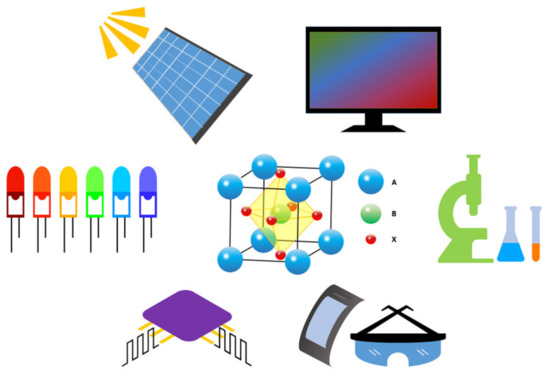
[5], while the organic examples include the methylammonium [6,7], formamidinium [8,9], and recently discovered methylhydrazinium [10,11]. It is expected that inorganic counterparts generally maintain better chemical stability than their organic counterparts [12]. When specified to the 3D LHPs, the materials have advantageous properties from more than one aspect, and people are eager to utilize them as working materials in various opto-electronic devices. In addition to solar cells [1,13], the materials are also utilized in lasers [7,14], light emitting diodes (LEDs) [15,16,17], photodetectors [18,19,20], modulators [21,22,23], and so on. Moreover, the materials, especially those with bromides, are found to exhibit outstanding nonlinear properties [10,24,25,26,27], thus demonstrating promising potential in applications such as imaging, optical limiting, and frequency conversion. Currently, people are incorporating the LHPs into waveguides and micro optical cavities, so as to further miniaturize the LHP-based devices. These efforts are leading to the emergence of integrated photonic/optical systems centering LHPs, which will play a significant role in next-generation opto-electronic applications, resulting in devices not only frequently used in the field of scientific research but also that of consumer electronics. In , the crystalline structure of LHP is presented in the center, which is surrounded by examples of potential applications for the LHP-based devices.
Figure 1.
Lead halide perovskites (LHPs) and their potential applications in various fields, including photovoltaic, illumination, communication, wearable devices, chemical test, and high-resolution display.
In addition to the prosperity of LHP material, novel opto-electronic materials including the atomically thin two-dimensional materials (2D) and one-dimensional (1D) materials are also rapidly growing. These materials, each with their unique properties in certain aspects, are also at the center of attention in the research community. LHPs, along with other materials, are all building blocks to construct devices. To some extent, people are free to choose from this “material bank” to fabricate devices and achieve better performances. In most cases, it is quite rigorous that a single species of material could cover all the application demands and introduce no impediments at the same time. On the other hand, it is more practical to combine different materials into the device and make them collaborate such that the advantages from the participants could be utilized, and the shortages could be made up to some extent. The LHP could be fabricated by solution-based methods and conveniently incorporated with semiconductors, metals, and polymers, making it very practical to construct LHP hybrid devices. By now, people have developed LHP hybrid devices covering lasers, photodetectors, modulators, and so on. The materials in collaboration with LHP include novel materials (for instance, graphene and 2D MoS
In addition to the prosperity of LHP material, novel opto-electronic materials including the atomically thin two-dimensional materials (2D) and one-dimensional (1D) materials are also rapidly growing. These materials, each with their unique properties in certain aspects, are also at the center of attention in the research community. LHPs, along with other materials, are all building blocks to construct devices. To some extent, people are free to choose from this “material bank” to fabricate devices and achieve better performances. In most cases, it is quite rigorous that a single species of material could cover all the application demands and introduce no impediments at the same time. On the other hand, it is more practical to combine different materials into the device and make them collaborate such that the advantages from the participants could be utilized, and the shortages could be made up to some extent. The LHP could be fabricated by solution-based methods and conveniently incorporated with semiconductors, metals, and polymers, making it very practical to construct LHP hybrid devices. By now, people have developed LHP hybrid devices covering lasers, photodetectors, modulators, and so on. The materials in collaboration with LHP include novel materials (for instance, graphene and 2D MoS2, etc.) and traditional materials (for instance, silicon). In these devices, the advantageous properties of participating materials are exploited, and the device performances have been improved substantially as compared to the devices made from single species of material. It is beneficial to retrospect these valuable works, which could light up more inspiration and enlightenment for future development in LHP hybrid devices.
2. The Properties of the LHP Materials
Due to the uniqueness of LHP, when a certain device is to be proposed, both the material’s opto-electronic property and its stability need to be considered carefully. In this part, the optical and electrical properties of LHP will be summarized, followed by the material’s property on stability.
2.1. Optical and Electrical Properties of LHP
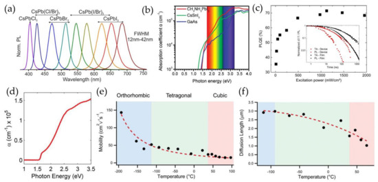
The LHPs are considered as outstanding candidates for next-generation opto-electronic applications, mostly due to the fact that the materials demonstrate outstanding optical and electrical properties in various aspects, as shown in . The LHPs are direct band-gap semiconductors, and the band-gap could be conveniently tuned by chemical composition (for instance, changing the halogen elements) and thus enabled to cover a wavelength range from visible to near-infrared [28,29]. The LHPs have large absorption coefficients. Taking CH3NH3PbI3 (MAPbI3) as an example, its absorption coefficient is found to be in the level of ~105 cm−1 in the visible range, being much larger than GaAs [30]. A large absorption coefficient, as well as a widely tunable bandgap, will contribute to a high-performance in photodetectors. LHPs also have high luminescence quantum yields. For solution-processed MAPbI3-xClx crystalline films as an example, a high photoluminescence (PL) quantum efficiency up to 70% has been reported [31]. MAPbI3 films have been found to demonstrate an outstanding gain of 3200 ± 830 cm−1, which is comparable to conventional light-emitting materials [32]. The high luminescence quantum yield along with the tunable band-gap, makes LHPs ideal candidates for applications including lasers and LEDs.
Figure 2. Optical and electrical properties of LHPs. (a) Representative photoluminescence (PL) spectra for CsPbX3Y3−z, where X and Y represents different halide elements, demonstrating a wide wavelength tunability for LHP. Reprinted with permission from [33]. Copyright 2015 American Chemistry Society (b) The absorption coefficient (α) of CH3NH3PbI3 (MAPbI3), CsSnI3 and GaAs. Reproduced with permission from [30].; published by Wiley, 2014. (c) The photoluminescence quantum efficiency (PLQE) of MAPbI3-xClx films. The inset shows the normalized PL intensity (integrated from 1.71 to 1.57 eV) and the transient absorption (TA) signal versus time for device and film samples. Reprinted with permission from [31] Copyright 2014 American Chemistry Society. (d) Absorption coefficient of MAPbI3 perovskite films, for which the absorption onset is at 1.55 eV. Reproduced with permission from [32].; published by Wiley, 2015. (e,f) mobility and diffusion of MAPbI3. In both panels, the black dots represent experimental data, and the regions marked by different colors from left to right correspond to orthorhombic, tetragonal, and cubic phase, respectively. The dashed lines in (e) is T−3/2 dependence prediction for band-like transport, and in (f) is an eye-guide. Reproduced with permission from [34]; published by Wiley, 2015.
LHPs are found to have high carrier mobility, long diffusion length, and low trap-related recombination rates [35,36,37]. These properties govern carriers’ transport dynamics which are important in applications such as photodetection. Carrier mobility and diffusion length are closely related to each other, and these two parameters show similar dependence on factors including crystalline quality and chemical composition [35]. The crystalline quality seems to be a dominant factor, and the mobility/diffusion length is much larger for single-crystal samples than its film counterparts. For instance, the hole mobility has been found to be ~164 cm2/(Vs) in solution-processed single-crystalline characterized using space charge limit current (SCLC) technique [38,39], which goes to ~0.4 cm2/(Vs) in poly-crystalline films [40]. The carrier diffusion length in MAPbI3 single crystals could be more than 175 μm [39], which could be reduced to 0.1 μm in MAPbI3 films [41]. Chemical composition tuning also enables the alteration of mobility and diffusion length. For instance, the diffusion length for MAPbI3−xClx is more than 1 μm [40], while in CH(NH2)2PbI3 (FAPbI3) films the effective diffusion length for electrons and holes are 177 ± 20 nm and 813 ± 72 nm, respectively [42]. When the film processing condition and procedures are optimized, the diffusion length could be further elongated [43,44]. The dependence mentioned above could be finally attributed to intrinsic factors such as Fröhlich interactions and extrinsic factors such as charge-carrier scattering by grain boundaries and dopants [45].
2.2. Intrinsic Instability of LHP
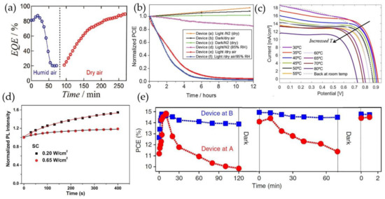
Although LHPs have novel properties leading to outstanding working performances in opto-electronic industry, the massive usage of the materials in practical occasions are mainly hindered by the severe instability of LHPs. As shown in , moisture, oxygen, elevated temperature, and light radiation are found to induce material degradation quite easily [46,47,48]. As for moisture and oxygen which is generally not necessary for device function, the corresponding degradation could be generally dealt with by insulation. For instance, it is required that the preparation of LHP–based solar cells should be in a relatively low humidity level of <1% atmosphere [49]. By careful encapsulation or introduction of hydrophobic contacts [50], device lifespan could be improved considerably. Unlike moisture and oxygen, heat is likely to accompany the device operation in some applications. The degree of heat-induced degradation is found to be dependent on chemical composition. For instance, while MAPbI3 will degrade at 85 ℃
[51], CsPbI3 could endure much higher temperature, showing stability up to 300 ℃
Figure 3. Instability of LHP induced by different environmental factors. (a) External quantum efficiency (EQE) as a function of exposure time to humid or dry air. Reproduced with permission from [53]; published by Wiley, 2016. (b) Evolution of the normalized power conversion efficiency (PCE) of FTO/cp-TiO2/mp-TiO2/MAPbI3/spiro-OMeTAD/Au devices in various environments. Illumination was performed with white LEDs equipped with ultraviolet (UV) filters. Reproduced with permission from [47]; published by The Royal Society of Chemistry, 2016. (c) I-V curves of a MAPbI3 Perovskite Solar Cells as a function of temperature. Reprinted with permission from [54]. Copyright 2016 American Chemistry Society. (d) PL intensities of the spin-coated MAPbI3 sample over time, under laser excitations at 0.2 and 0.65 W/cm2, respectively. Reproduced with permission from [55]; published by Wiley, 2016. (e) The PCE evolution with time under 1-sun illumination and after resting the device in dark, when the device is stressed at point A (red circles, J = 0, V = Voc) or at point B (blue squares, J = JSC, V = 0) between each data point. Reproduced with permission from [47]; published by Springer Nature, 2016.
Light-induced degradation of LHP may be the most intractable problem, since light radiation is a necessity for most of the LHP-based devices to function properly. Researchers have found that the detailed degradation depend significantly on factors including illumination time, power density, and wavelength. When the device is exposed to relatively low power density for a short time, the so-called photo-curing effect is likely to occur, leading to substantial enhancements in PL intensity as well as devices’ working performances [56,57]. However, the enhancements could not last long. With the further extension of illumination time, apparent degradation could be observed [47,58,59]. When the illumination power density increases even higher, the degradation accelerates, and structure transformation could be easily exhibited by characterization techniques such as Raman spectroscopy [60,61,62,63,64]. LHP may recover after being placed in dark for a certain period of time; however, the recovery reported varies from different research groups [47,58]. The illumination wavelength has been also found to have apparent influence on LHP’s degradation. Both ultraviolet (UV) [65,66,67,68] and infrared (IR) light [58] has been found to accelerate the degradation of solar cells, attributed to different physical mechanisms. By now, people have proposed explanations such as ion-migration and light-induced trap states [12,47,67,69,70,71], but no census has been reached yet. The light-induced degradation turns out to be a very complex process, and it is possible that the degradation involves more than one contributing mechanism simultaneously.
In a nutshell, LHP tends to degrade easily in environmental factors including humidity, oxygen, heat, and light. When the corresponding material is to be grown or the device to be designed and fabricated, people need to maintain a good awareness of the instability of LHP, so as to ensure that the LHP is not damaged during fabrication and stay undegraded as long as possible.
3. The LHP Based Functional Devices
3.1. Lasers
3.1.1. Lasers and Factors Influencing their Performances
LHPs are ideal candidates for gain materials in next-generation lasers. By now, a diversity in different lasing configurations has been enjoyed, which could be referred to in Figure 4. As an instance, Saliba et al., 2016 put forward a general structuring approach for a LHP-based distributed feedback (DFB) laser by evaporating the MAPbI3 film onto a nanoimprinted polymer gratings with different pitches (Λ) [72]. The laser emission wavelength could be altered in the range of 770–793 nm by tuning the grating periodicity. A threshold in the level of ~μJ/cm2 has been found when pumped by a 532 nm nanosecond pulsed laser. Chen et al., on the other hand, reported a LHP photonic crystal (PhC) laser, fabricated by depositing the MAPbI3 thin films onto a 2D quartz PhC resonator [7]. In the PhC cavity, light-matter interaction could be enhanced via the in-plane distributed feedback, and single mode lasing could be achieved by appropriately matching the PhC band edge mode with the gain band of LHP. The device exhibited an output beam with a coherent and well-defined spatial profile, showing a small angular divergence (<2°) in the far-field pattern. The laser demonstrated a threshold of 68.5 μJ/cm2 when pumped by a 532 nm laser with 270 ps duration and showed a differential quantum efficiency of 35.8 ± 5.4%. By now, in addition to DFB lasers [8,72–76] and PhC lasers [2,7], LHP have also been utilized in lasers including whispering gallery mode (WGM) lasers [77], vertical cavity surface-emitting lasers (VCSEL) [5,14,78,79], and so on. The detailed parameters regarding LHP-based lasers’ performances are presented in Table 1.
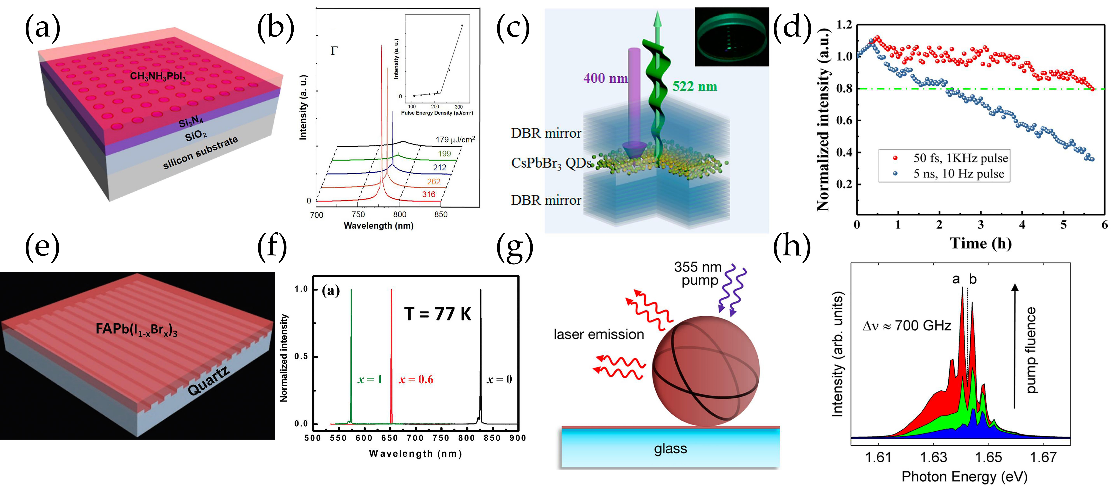
Figure 4. Lasing in LHP with various types of micro/nano structures. (a) Schematic diagram of a MAPbI3 photonic crystal (PhC) band edge laser. (b) The lasing spectra versus the pump intensity, and the intensities were extracted and shown in the inset. Reprinted from [2], with the permission of AIP Publishing. (c) Schematic diagram of the CsPbBr3 quantum dot (QD) vertical cavity surface-emitting lasers (VCSEL) (Inset: a photograph of the device in operation.). (d)The stability characterization for the laser under nanosecond/femtosecond pump light, revealing a longer lifespan for the femtosecond pumping condition. Reprinted with permission from [5]. Copyright 2017 American Chemistry Society. (e) Schematic illustration of a LHP alloy distributed feedback (DFB) laser. (f) The lasing spectra with varying chemical compositions, at 77K. Reproduced with permission from [8]; published by Wiley, 2017. (g) Lasing in a MAPbI3-covered sphere resonator. (h) The emission spectra under different pump fluences. Reprinted with permission from [80]. Copyright 2014 American Chemistry Society.
3.2. Photodetectors
Photodetectors are devices that convert optical signals to electrical signals, which are one of the key components used in areas including communication, sensing, imaging, and computation. People have proposed photodetectors by combining LHP with 2D and 1D materials to realize high performance and broad working range. As presented in Figure 6, bending of the electronic band at the interface is the key to realize high performance photodetection. By combining LHP with the other species of material, enhancement in the effective absorption coefficient and/or absorption bandwidth could be achieved. The device performances for some of the recent LHP photodetectors are presented in Figure 7, and the parameters are summarized in Table 2.
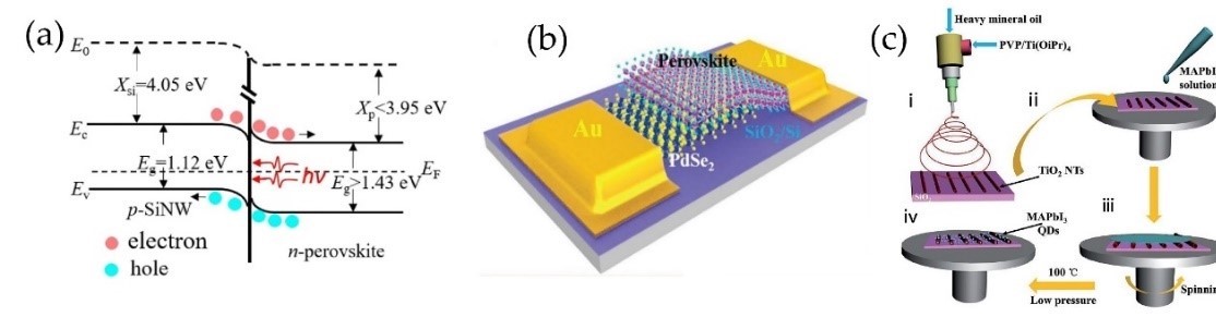
Figure 6. (a) The bending of energy band at the interface of the LHP based photodetector. Reprinted with the permission from [9]. Copyright 2018 American Chemistry Society. (b) Schematic illustration of a hybrid photodetector by combining perovskite with the 2D PdSe2. Reproduced with permission from [91]; published by Wiley, 2019. (c) The fabrication process for a LHP/TiO
2, etc.) and traditional materials (for instance, silicon). In these devices, the advantageous properties of participating materials are exploited, and the device performances have been improved substantially as compared to the devices made from single species of material. It is beneficial to retrospect these valuable works, which could light up more inspiration and enlightenment for future development in LHP hybrid devices.
nanotubes (NTs) photodetector. Reproduced with permission from [81]; published by Wiley, 2017.
3.3. Modulators
Modulators and switches are common optical components found in integrated optical circuits. These days, LHP have been utilized to construct modulators or switches working in THz range, for which the corresponding working principle is presented in Figure 8. The light modulation or switching by LHP hybrid devices are based on the THz absorption by charge carriers. By combining LHP with a proper material (for instance, silicon has been frequently used), a heterostructure is produced, of which the electronic structure bends at the interface. When pump light is turned on, photogenerated carriers are to be excited and tend to drift to the interface and accumulate there. When the THz waves are incident at the devices, the wave will be attenuated by the carriers, through mechanisms including electron-hole scattering, electron-phonon scattering, and electron-impurity scattering [112]. The actual absorption coefficient of the device changes in correspondence to pump laser. Consequently, the intensity of the incident THz waves is modulated. In Table 3, the performance from some of the recent LHP THz modulators is presented.
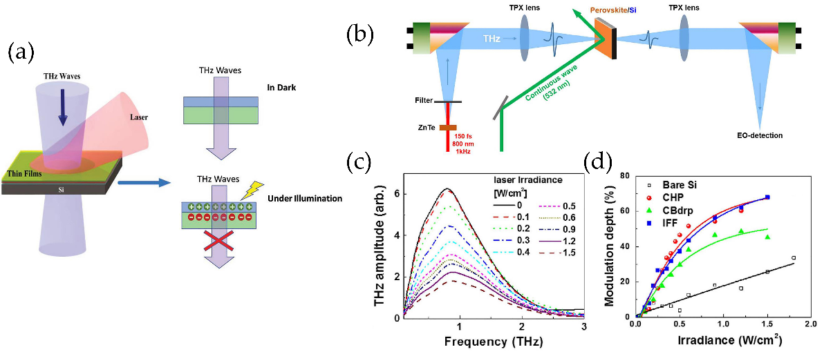
Figure 8. (a) Operation mechanism of the all-optical THz modulator under laser irradiation Reproduced with permission from [21]; published by Wiley, 2020. (b) Schematic of the THz all-optical modulation measurement; (c) THz transmittance under different laser irradiance and (d) the corresponding modulation depth (MD). Reproduced with permission from [22]; published by Springer Nature, 2016.