Optical spectrometers and sensors have gained enormous importance in metrology and information technology, frequently involving the question of size, resolution, sensitivity, spectral range, efficiency, reliability, and cost. Nanomaterials and nanotechnological fabrication technologies have huge potential to enable an optimization between these demands, which in some cases are counteracting each other. This paper focuses on the visible and near infrared spectral range and on five types of optical sensors (optical spectrometers): classical grating-based miniaturized spectrometers, arrayed waveguide grating devices, static Fabry–Pérot (FP) filter arrays on sensor arrays, tunable microelectromechanical systems (MEMS) FP filter arrays, and MEMS tunable photonic crystal filters. The comparison between this selection of concepts concentrates on (i) linewidth and resolution, (ii) required space for a selected spectral range, (iii) efficiency in using available light, and (iv) potential of nanoimprint for cost reduction and yield increase.
- nanoimprint
- photonic nanomaterials
- optical spectrometers
- interferometers
- Fabry–Pérot filters
- detector arrays
- tunable MEMS
- linewidth
- miniaturization
1. Introduction
Smart system integration and smart personal environments are gaining increasing interest. Photonic methodologies enable applications such as smart sensing and high bitrate information technologies with distinct characteristics of small footprint and lightweight via miniaturization, enabling low-cost, high accuracy, and sufficient efficiency. Optical spectroscopy [1][2][3][4][5][6][7][8][9][10] reveals high sensitivity and remarkable selectivity with wide application fields [1], including industrial production control, environmental monitoring, agriculture growth monitoring, medical diagnosis and medical prevention, and communication technologies, to name a few. Some of the optical sensors use nanomaterials and are already integrated into smart personal environments or have high potential to be integrated into those in the future. However, counter-running demands are often involved, for example, concerning size and resolution.
Smart system integration and smart personal environments are gaining increasing interest. Photonic methodologies enable applications such as smart sensing and high bitrate information technologies with distinct characteristics of small footprint and lightweight via miniaturization, enabling low-cost, high accuracy, and sufficient efficiency. Optical spectroscopy [1,2,3,4,5,6,7,8,9,10] reveals high sensitivity and remarkable selectivity with wide application fields [1], including industrial production control, environmental monitoring, agriculture growth monitoring, medical diagnosis and medical prevention, and communication technologies, to name a few. Some of the optical sensors use nanomaterials and are already integrated into smart personal environments or have high potential to be integrated into those in the future. However, counter-running demands are often involved, for example, concerning size and resolution.
This study starts with an introduction of optical spectrometers and methodologies of spectroscopy for the ultraviolet (UV), visible (VIS), and near infrared (NIR) spectral wavelengths range. Classical spectrometers [4][8][9][10] use prisms or gratings (diffractive elements) to disperse the studied optical signal in an intensity profile as a function of wavelength (spectrum). The higher the order in grating spectrometers, the higher the resolution but the smaller the intensity. Therefore, in many cases the gratings are blazed—meaning that they exhibit a sawtooth structure—to shift the high intensities from zero order into the first or higher diffraction orders [4]. This is a good compromise to benefit from relatively high resolution and relatively high intensity. Microelectromechanical systems (MEMS) can be used to miniaturize grating spectrometers. Electrostatic MEMS actuation has been demonstrated for different material systems and wavelength ranges to rotate the grating [11][12][13][14].
This study starts with an introduction of optical spectrometers and methodologies of spectroscopy for the ultraviolet (UV), visible (VIS), and near infrared (NIR) spectral wavelengths range. Classical spectrometers [4,8,9,10] use prisms or gratings (diffractive elements) to disperse the studied optical signal in an intensity profile as a function of wavelength (spectrum). The higher the order in grating spectrometers, the higher the resolution but the smaller the intensity. Therefore, in many cases the gratings are blazed—meaning that they exhibit a sawtooth structure—to shift the high intensities from zero order into the first or higher diffraction orders [4]. This is a good compromise to benefit from relatively high resolution and relatively high intensity. Microelectromechanical systems (MEMS) can be used to miniaturize grating spectrometers. Electrostatic MEMS actuation has been demonstrated for different material systems and wavelength ranges to rotate the grating [11,12,13,14].
2. Static FP Filter Arrays on Photodetector Arrays
2.1. Microspectrometers
An FP filter consists of two highly reflective mirrors and a transparent resonance cavity layer in between. The transmitted narrow spectral band is indicated as filter transmission line and the spectral transmission peak is the maximum of this line. Its spectral position is related to the vertical extension or height of the respective cavity—the higher the cavity, the longer the wavelength of the transmitted peak. The highly reflective mirrors are predominantly dielectric DBRs. Each DBR comprises a periodic stack of alternating thin films with low and high optical refractive indices. It can form a high reflective spectral band—the so-called stopband. The stopband width is determined by the contrast of refractive indices of the two chosen materials, i.e., the larger the contrast, the wider the stopband.
A microspectrometer is the combination of FP filter array and corresponding detector array. Since the size reduction of conventional grating-based spectrometers is accompanied by an enormous decrease in optical resolution, the FP filter-array-based spectrometers are an interesting alternative because they do not suffer from resolution decrease [15][16][17][18]. However, these existing FP filter-array-based microspectrometers [15][16][17][18] may require complicated fabrication steps for patterning of various 3D filter cavities with different heights, which is not cost efficient for industrial fabrication. Up to now, different methodologies have been applied to define the different cavity heights, i.e., the resonance cavities of FP filter arrays. Correia et al. [15][16] used
A microspectrometer is the combination of FP filter array and corresponding detector array. Since the size reduction of conventional grating-based spectrometers is accompanied by an enormous decrease in optical resolution, the FP filter-array-based spectrometers are an interesting alternative because they do not suffer from resolution decrease [27,28,29,30]. However, these existing FP filter-array-based microspectrometers [27,28,29,30] may require complicated fabrication steps for patterning of various 3D filter cavities with different heights, which is not cost efficient for industrial fabrication. Up to now, different methodologies have been applied to define the different cavity heights, i.e., the resonance cavities of FP filter arrays. Correia et al. [27,28] used
digital etching to create 16 different FP cavity heights with four lithography/etching steps (16 pixels). Wang et al. 2007 [18] used
to create 16 different FP cavity heights with four lithography/etching steps (16 pixels). Wang et al. 2007 [30] used
digital deposition
to create 128 different FP cavity heights with nine lithography/deposition steps (128 pixels). The
digital masking
shown in
enables
digital etching if it is combined with subsequent etching steps [15][16], and enables
if it is combined with subsequent etching steps [27,28], and enables
digital deposition if it is combined with subsequent deposition steps [18]. It is obvious, the more different cavity heights that exist in an FP filter array, the more filter transmission lines can be obtained.
if it is combined with subsequent deposition steps [30]. It is obvious, the more different cavity heights that exist in an FP filter array, the more filter transmission lines can be obtained.
2.2. Nanospectrometers
For the purpose of simplifying the fabrication of cavities, we proposed a FP filter array [19][20][21], which contains nanoimprinted transparent resonance cavities with distinct heights and two identical high-optical-quality DBRs. Since nanoimprint technology is used, we introduced it as nanospectrometer, which combines a FP filter array and a detector array.
For the purpose of simplifying the fabrication of cavities, we proposed a FP filter array [31,32,33], which contains nanoimprinted transparent resonance cavities with distinct heights and two identical high-optical-quality DBRs. Since nanoimprint technology is used, we introduced it as nanospectrometer, which combines a FP filter array and a detector array.
a depicts four FP filters as a part of the whole array. A filter array consists of two identical dielectric DBRs (gray) and nanoimprinted transparent cavities (shown orange). Each individual cavity height corresponds to a half wavelength of the filter line in the medium. Thus, each height determines the wavelength of the individual narrow transmission line of the specific single filter. The filter array will be directly deposited on a detector array (black and magenta). Each FP filter corresponds to one detector (
a). However, a single square filter can also correspond to a multiple of detector pixels (4, 9, 16, …). It is important to note that the cavity height determines the spectral position of the filter transmission line within the stopband. The right part of
a shows the spectral transmission of 4 FP filters with identical range of minimum transmission (stopband) and varied spectral position of the filter line (due to tailored cavity heights). A 3D nanoimprint allows fabrication of all different cavities in a single step.
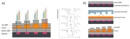
Figure 1.
(
a
) Schematic design of a Fabry–Pérot filter-array-based nanospectrometer (left) and its corresponding calculated transmission spectra (right). (
b
) Fabrication process involving substrate conformal imprint lithography (SCIL).
We used 3D nanoimprint with a single imprint step to structure 192 different cavity heights (192 pixels), which otherwise requires extensive and repetitive fabrication steps. This negates the need for time-consuming digital etching [15][16] or digital deposition [18] in the FP filter array fabrication. Besides, it is more cost efficient since the digital etching is transferred into the fabrication of a 3D nanoimprint template, which can be reused multiple times in the production. For more than 16 pixels, application of digital procedures directly in the array fabrication is cost inefficient and unsuitable for industrial fabrication.
We used 3D nanoimprint with a single imprint step to structure 192 different cavity heights (192 pixels), which otherwise requires extensive and repetitive fabrication steps. This negates the need for time-consuming digital etching [27,28] or digital deposition [30] in the FP filter array fabrication. Besides, it is more cost efficient since the digital etching is transferred into the fabrication of a 3D nanoimprint template, which can be reused multiple times in the production. For more than 16 pixels, application of digital procedures directly in the array fabrication is cost inefficient and unsuitable for industrial fabrication.
Figure 1b displays the main fabrication steps from top to bottom, starting with the bottom DBR deposition. The liquid cavity material (orange) is deposited by spin-coating. The 3D cavity structure is formed by the transparent 3D stamp (light blue) pressed into the cavity material and hardened under UV radiation. After releasing the stamp, the top DBR is deposited. Nanoimprint is a molding technology for patterning deformable materials, usually polymers. Various nanoimprint technologies [22][23][24][25] have been developed for the purpose of generating 2D structures with high lateral resolution. However, for our nanospectrometer, it is also crucial to accurately control the vertical resolution (3D). To enable mass production, a master template (positive) revealing the checkerboard-type arranged mesa structures (different cavity heights) is replicated into numerous identical stamps (negative). The 3D nanoimprint is performed using one of these stamps, forming the orange 3D cavity structures (shown in
b displays the main fabrication steps from top to bottom, starting with the bottom DBR deposition. The liquid cavity material (orange) is deposited by spin-coating. The 3D cavity structure is formed by the transparent 3D stamp (light blue) pressed into the cavity material and hardened under UV radiation. After releasing the stamp, the top DBR is deposited. Nanoimprint is a molding technology for patterning deformable materials, usually polymers. Various nanoimprint technologies [75,76,77,78] have been developed for the purpose of generating 2D structures with high lateral resolution. However, for our nanospectrometer, it is also crucial to accurately control the vertical resolution (3D). To enable mass production, a master template (positive) revealing the checkerboard-type arranged mesa structures (different cavity heights) is replicated into numerous identical stamps (negative). The 3D nanoimprint is performed using one of these stamps, forming the orange 3D cavity structures (shown in
) simultaneously in a single step. Note that the process described here is for a single stopband. In the upcoming
, a proof-of-principle method to simultaneously print with a single nanoimprint step on three different bottom DBR stacks is reported. This involves three different stopbands and prints over vertical steps occurring at the connection faces of the stacks.
We conclude that unlike grating spectrometers, the nanospectrometer is not affected by the decreasing optical resolution due to miniaturization, and it requires only a single step to define the complex 3D cavity layer, independent of the number of pixels.
3. FP Filter Arrays for the NIR: Fabrication and Characterization
The FP filter arrays are designed for the 1.4–1.5 µm spectral range. For the bottom and top DBR, 9.5 periods of Si
3
N
4
/SiO
2
are deposited by PECVD. These DBRs are deposited at a temperature of 120 °C to avoid higher temperature exposure to the polymeric 3D cavity layer. The resist mr-NIL210 is used in a single spin-coating process to obtain cavity heights much larger than required in the previous sections for the VIS spectral range. Each filter has lateral dimensions of 40 × 40 µm
2
, and the vertical dimension of the imprinted structures varies between 365 and 530 nm.
For optical characterization, a supercontinuum laser, edge filters, two confocal microscope objectives, and a photodiode array are used.
Figure 2a depicts optical transmission spectra of FP filter arrays via a selection of some typical filter transmission lines (as representatives) out of 64 spectrally different lines to avoid overloading the figure. High maximum transmission up to 90% and average transmission values well above 70% are observed. The FWHMs of all filter transmission lines are between 4.7 and 8.2 nm and the smallest FWHM is achieved at 1450 nm. This provides a resolution—defined as the ratio of the transmission wavelength and the FWHM—of 300. In
9a depicts optical transmission spectra of FP filter arrays via a selection of some typical filter transmission lines (as representatives) out of 64 spectrally different lines to avoid overloading the figure. High maximum transmission up to 90% and average transmission values well above 70% are observed. The FWHMs of all filter transmission lines are between 4.7 and 8.2 nm and the smallest FWHM is achieved at 1450 nm. This provides a resolution—defined as the ratio of the transmission wavelength and the FWHM—of 300. In
Figure 2b, the experimental FWHMs are compared to the results of theoretical model calculations. For the simulation we used “OpenFilters” and experimental material parameters for spectral material dispersion
9b, the experimental FWHMs are compared to the results of theoretical model calculations. For the simulation we used “OpenFilters” and experimental material parameters for spectral material dispersion
n
(
λ
) and spectral absorption
α
(
λ
) obtained by spectroscopic ellipsometry. The discussion of the FWHM variation has already been done in
, yet we would like to add some remarks concerning the related interface roughness. The surface roughness of layered heterostructures is investigated on the resist mr-UVCur06 using atomic force microscopy (AFM). We observed an rms value of below 4 nm for a single layer and 8 nm for a double layer. This is qualitatively in agreement with our observations since in layered heterostructures, this measured surface roughness is incorporated and slightly modified into interface roughness. Furthermore, surface roughness and interface roughness between layers exist for each SiO
2
layer deposited by PECVD. The larger the number of layers included in our cavity, the more interfaces are present, and thus the higher the final accumulation of interface roughness.
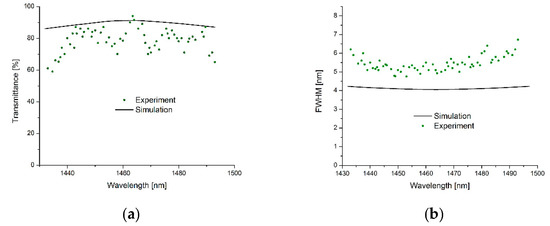
Figure 29.
(
a
) Comparison of measured maximum transmission (symbols) of the filter lines of an FP filter array for the NIR spectral range with simulated data (full lines). (
b) Comparison of measured FWHM (symbols) and simulated FWHM (full lines) of the same FP filter array. The corresponding Transfer Matrix simulations include experimental data for spectral absorption and spectral dispersion. Reproduced with permission from [26] © Springer Applied Nanoscience, 2016.
) Comparison of measured FWHM (symbols) and simulated FWHM (full lines) of the same FP filter array. The corresponding Transfer Matrix simulations include experimental data for spectral absorption and spectral dispersion. Reproduced with permission from [35] © Springer Applied Nanoscience, 2016.
Next, the sensitivity of the spectrometer including FP filter arrays against temperature changes is considered. Assuming similar thermal conductivities of the layer materials involved, the interfaces included in the heterostructure might reduce the overall thermal conductivity across the interfaces considerably. A clear and distinct conclusion as well as a full understanding of the impact of interfaces is not yet revealed in the literature [27]. However, most of the studies presented up to now reveal a rule of thumb: the thermal conductivity decreases with rising number of interfaces [27], and the first interface most likely provides the largest heat resistance compared to the last interface of multiple interfaces. Therefore, in the case of only a few interfaces, the difference in thermal resistivity between a single interface and three interfaces is expected to be noticeable. In addition, a multiple cavity layer design may potentially reduce the overall temperature expansion coefficient, if materials of positive and negative coefficients are used in combination. Nonetheless, it is hard to find materials of negative thermal expansion coefficients like yttrium oxide.
Next, the sensitivity of the spectrometer including FP filter arrays against temperature changes is considered. Assuming similar thermal conductivities of the layer materials involved, the interfaces included in the heterostructure might reduce the overall thermal conductivity across the interfaces considerably. A clear and distinct conclusion as well as a full understanding of the impact of interfaces is not yet revealed in the literature [83]. However, most of the studies presented up to now reveal a rule of thumb: the thermal conductivity decreases with rising number of interfaces [83], and the first interface most likely provides the largest heat resistance compared to the last interface of multiple interfaces. Therefore, in the case of only a few interfaces, the difference in thermal resistivity between a single interface and three interfaces is expected to be noticeable. In addition, a multiple cavity layer design may potentially reduce the overall temperature expansion coefficient, if materials of positive and negative coefficients are used in combination. Nonetheless, it is hard to find materials of negative thermal expansion coefficients like yttrium oxide.
4. Fabrication and Characterization of MEMS Tunable FP Filters in the NIR Range
Si-based CCD or CMOS photodetector arrays cannot be used for the 1.2–2 µm infrared spectral range, so a more expensive IR detector arrays based on InGaAs must be used instead. To reduce cost of IR spectrometers, MEMS spectrally tunable devices are very attractive. A larger spectral range of 1.15–1.8 µm (650 nm span) can, e.g., be bridged using a small array of only three InGaAs photodiodes and three corresponding MEMS tunable filters, which are spectrally neighbored and each tuning range is over 220 nm respectively. Many different designs of MEMS tunable filters in various material systems have been reported [28][29][30][31][32][33][34][35][36][37][38][39][40][41][42][43][44][45][46][47]. As an example, Figure 12a displays an SEM micrograph top-view of one of our InP-multiple airgap MEMS FP filters; circular central membranes are elastically fixed by four suspensions to four supporting posts. In general, there are many design options for MEMS tunable filters, and two of them are presented in this paper.
Si-based CCD or CMOS photodetector arrays cannot be used for the 1.2–2 µm infrared spectral range, so a more expensive IR detector arrays based on InGaAs must be used instead. To reduce cost of IR spectrometers, MEMS spectrally tunable devices are very attractive. A larger spectral range of 1.15–1.8 µm (650 nm span) can, e.g., be bridged using a small array of only three InGaAs photodiodes and three corresponding MEMS tunable filters, which are spectrally neighbored and each tuning range is over 220 nm respectively. Many different designs of MEMS tunable filters in various material systems have been reported [37,38,39,40,41,42,43,44,45,46,47,48,49,50,51,52,53,54,55,56]. As an example, Figure 12a displays an SEM micrograph top-view of one of our InP-multiple airgap MEMS FP filters; circular central membranes are elastically fixed by four suspensions to four supporting posts. In general, there are many design options for MEMS tunable filters, and two of them are presented in this paper.
Figure 3 depicts a first option with a single airgap, where the lower DBR is attached to the substrate (not shown) and remains flat. Only the top DBR is electrostatically or thermally actuated. By varying the airgap cavity height, all incoming wavelengths are reflected except the one constituting a multiple of a half wavelength in the cavity. This wavelength (more precisely a small transmission line with this wavelength in the center) is transmitting the filter. The disadvantages of this design are (i) the relatively thick (and thus stiff) DBR stacks require long suspensions to allow the necessary large membrane displacement and to enable a large tuning range, and (ii) limited stopband widths.
10 depicts a first option with a single airgap, where the lower DBR is attached to the substrate (not shown) and remains flat. Only the top DBR is electrostatically or thermally actuated. By varying the airgap cavity height, all incoming wavelengths are reflected except the one constituting a multiple of a half wavelength in the cavity. This wavelength (more precisely a small transmission line with this wavelength in the center) is transmitting the filter. The disadvantages of this design are (i) the relatively thick (and thus stiff) DBR stacks require long suspensions to allow the necessary large membrane displacement and to enable a large tuning range, and (ii) limited stopband widths.
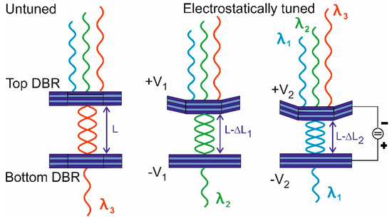
Figure 310.
MEMS tunable FP filters with a single airgap. Examples for material systems are GaAs/AlAs, SiO
2
/Si
3
N
4
, or SiO
2
/TiO
2
. In this figure, a four-times half-wavelength (4∙
λ
/2) cavity and electrostatic actuation is shown. The required partial metal layers are not drawn.
Note that there also other options for MEMS tunable filters based on the thickness actuation of solid components of the filter [48]. However, this review focuses on the thickness actuation of an airgap cavity.
Note that there also other options for MEMS tunable filters based on the thickness actuation of solid components of the filter [57]. However, this review focuses on the thickness actuation of an airgap cavity.
Figure 4 depicts a second airgap-based option that overcomes the abovementioned disadvantage resulting from thick layer stacks (
11 depicts a second airgap-based option that overcomes the abovementioned disadvantage resulting from thick layer stacks (
Figure 3). In addition, this second option enables much larger stopband widths. Due to the large refractive index contrast of 1 (air) to 3.167 (InP) between the two DBR materials at
10). In addition, this second option enables much larger stopband widths. Due to the large refractive index contrast of 1 (air) to 3.167 (InP) between the two DBR materials at
λ
= 1.55 µm, very large stopbands are usable: 500 nm for
λair
/4 with 3
λInP
/4 and even 1500 nm for
λair
/4 with
λInP/4. A DBR with 2.5 periods of InP/air already provides a reflectivity of 99.8%. The n-doping of top DBR and p-doping of bottom-DBR allows actuation of the airgap cavity via the applied actuation voltage. Our group and others have reported on micromachined InP/airgap DBR-based vertical-cavity tunable filters by different approaches [32][35][36][37][38][39][40][41][42][43][44][45][46][47]. Due to shielding effects, the charges are mainly located at the inside surfaces of the two central membranes. Therefore, only these two membranes are mainly actuated. Comparing this with the “unobtainable situation” where all InP membranes of each DBR are actuated simultaneously, we only suffer from a 10% smaller tuning range, which we derived from detailed theoretical model calculations with a Transfer Matrix-based tool. We fabricated multiple design variants differing in membrane diameter and suspension lengths.
/4. A DBR with 2.5 periods of InP/air already provides a reflectivity of 99.8%. The n-doping of top DBR and p-doping of bottom-DBR allows actuation of the airgap cavity via the applied actuation voltage. Our group and others have reported on micromachined InP/airgap DBR-based vertical-cavity tunable filters by different approaches [41,44,45,46,47,48,49,50,51,52,53,54,55,56]. Due to shielding effects, the charges are mainly located at the inside surfaces of the two central membranes. Therefore, only these two membranes are mainly actuated. Comparing this with the “unobtainable situation” where all InP membranes of each DBR are actuated simultaneously, we only suffer from a 10% smaller tuning range, which we derived from detailed theoretical model calculations with a Transfer Matrix-based tool. We fabricated multiple design variants differing in membrane diameter and suspension lengths.
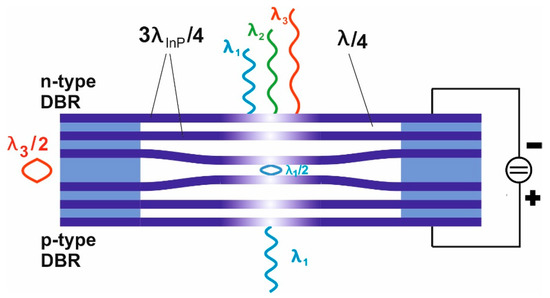
Figure 411.
MEMS tunable FP filters with multiple airgaps and InP membranes and suspensions. The supporting posts consist of the corresponding InP/InGaAs multilayer stack. Partly, InGaAs is used as sacrificial layer.
Each DBR consists of 3
λInP
/4 InP membranes and two
λ
/4 airgaps. InGaAs serves as sacrificial layers and parts of the supporting posts. The InP/GaInAs layer stack was epitaxially grown by MOCVD. The filters were fabricated using photolithography and subsequent vertical dry etching (RIE H
2
/CH
4
/Ar), followed by a second lithography to mask the supporting posts. The airgaps and central air were formed by selectively under-etching the GaInAs sacrificial layers using FeCl
3
etchant. The filter has membranes of 20 µm diameter with four suspensions of 30 µm length and 10 µm width that connect the membrane to supporting posts. SEM micrographs of a filter structure are shown in
Figure 5a,b.
12a,b.
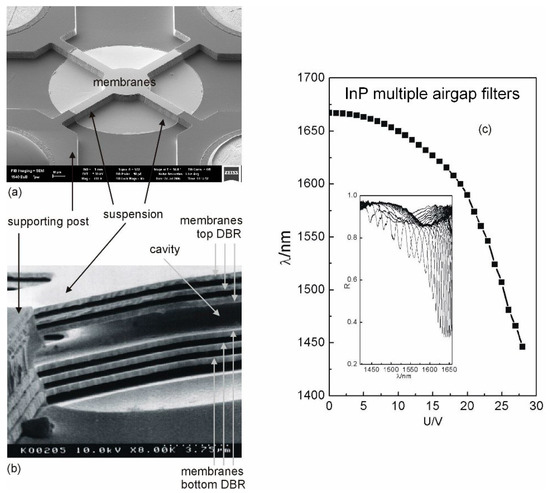
Figure 512.
(
a
) SEM micrograph of an InP/InGaAs multiple airgap MEM tunable FP filter. (
b
) SEM micrograph from the side, allowing the view through the airgaps between the suspensions. (
c
) Wavelength of the filter peak wavelengths as a function of actuation voltage. The inset displays a selection of measured reflection spectra
R
(
λ
) recorded as a function of the actuation voltage
U
.
The filter (resonant) wavelength as a function of actuation voltage is shown in
Figure 5c. The inset shows the corresponding reflectance spectra. The tuning characteristics of the filters show a very large tuning range of 221 nm [46] for the actuation voltage of 28 V. To the best of our knowledge, this is the widest experimental tuning range reported for the InP/multiple airgap DBR-based vertical-cavity filters. The FWHM is narrow (typically 1 nm) at lower actuation voltage; however, it increases at higher actuation voltage due to deformation of the membranes. The record FWHM value that we measured in InP multiple airgap FP filters was 0.1 nm at 1.55 µm. Thus, the potential optical resolution of the FP filter methodology might be 15,000 in the best case.
12c. The inset shows the corresponding reflectance spectra. The tuning characteristics of the filters show a very large tuning range of 221 nm [55] for the actuation voltage of 28 V. To the best of our knowledge, this is the widest experimental tuning range reported for the InP/multiple airgap DBR-based vertical-cavity filters. The FWHM is narrow (typically 1 nm) at lower actuation voltage; however, it increases at higher actuation voltage due to deformation of the membranes. The record FWHM value that we measured in InP multiple airgap FP filters was 0.1 nm at 1.55 µm. Thus, the potential optical resolution of the FP filter methodology might be 15,000 in the best case.
The InP material system has been chosen to enable monolithic integration with InGaAs photodiodes for telecommunication NIR wavelengths. A laboratory demonstrator with monolithically integrated MEMS tunable FP filters and InGaAs photodiodes was found to be operable. Furthermore, a packaged tunable filter with two fiber pigtails has been demonstrated for the InP/multiple airgap material system.
To avoid the sacrificial layer in 3D nanoimprint, we transferred a technique introduced by Cheng et al. [49] using selective curing in silica templates into our hybrid SCIL templates [50]. Utilization of UV-blocking metal layers enables us to define areas with noncured nanoimprint resist. Thus, cured hard resist remains only in the area of supporting posts, while other areas with noncured resist show a nonexistent residual layer upon the resist removal. This was a breakthrough in nanomaterials and our SCIL 3D nanoimprint lithography [50].
To avoid the sacrificial layer in 3D nanoimprint, we transferred a technique introduced by Cheng et al. [84] using selective curing in silica templates into our hybrid SCIL templates [85]. Utilization of UV-blocking metal layers enables us to define areas with noncured nanoimprint resist. Thus, cured hard resist remains only in the area of supporting posts, while other areas with noncured resist show a nonexistent residual layer upon the resist removal. This was a breakthrough in nanomaterials and our SCIL 3D nanoimprint lithography [85].
We have shown in our PC MEMS tunable filters the narrowband filters that additionally provide polarization selective properties. This maintains the compactness of MEMS devices by introducing a PC structure with strongly elliptical holes in the top membrane of the top DBR. The most common approaches are to use guided-mode resonance structures [51][52][53] or structural birefringence [54]. The selectivity towards the electric field orientation of the incident wave is in both cases achieved by breaking the 90° symmetry in line gratings or with elliptical elements of photonic crystals.
We have shown in our PC MEMS tunable filters the narrowband filters that additionally provide polarization selective properties. This maintains the compactness of MEMS devices by introducing a PC structure with strongly elliptical holes in the top membrane of the top DBR. The most common approaches are to use guided-mode resonance structures [62,63,65] or structural birefringence [66]. The selectivity towards the electric field orientation of the incident wave is in both cases achieved by breaking the 90° symmetry in line gratings or with elliptical elements of photonic crystals.
5. Resolution Limits of 3D Nanoimprint Lithography
In 2D nanoimprint lithography, the smallest lateral structures of 5 nm have been printed using a MBE-grown GaAs/AlAs heterostructure that is cleaved and selectively etched on the cleaved side, and the side is used as a nanoimprint template [55]. Using a carbon nanotube as a template in the lateral direction, structures as small as 2 nm could be demonstrated [56]. Theoretical model calculations [57][58] were performed, including most of the important forces between all the individual atoms on the nanoscale surface of the template and those atoms on the surface of the imprint resist. This group found that for structures revealing lateral dimensions below 0.5 nm, the template cannot be removed any more from the imprinted and hardened resist. Thus, this could be defined as the limit for size reduction in nanoimprint lithography.
In 2D nanoimprint lithography, the smallest lateral structures of 5 nm have been printed using a MBE-grown GaAs/AlAs heterostructure that is cleaved and selectively etched on the cleaved side, and the side is used as a nanoimprint template [86]. Using a carbon nanotube as a template in the lateral direction, structures as small as 2 nm could be demonstrated [87]. Theoretical model calculations [88,89] were performed, including most of the important forces between all the individual atoms on the nanoscale surface of the template and those atoms on the surface of the imprint resist. This group found that for structures revealing lateral dimensions below 0.5 nm, the template cannot be removed any more from the imprinted and hardened resist. Thus, this could be defined as the limit for size reduction in nanoimprint lithography.
However, this result seems to be in contradiction to the smallest height differences we obtained between neighboring mesa structures [20][21] in our templates used for the 3D nanoimprint fabrication of our FP filter arrays. The best transmission lines spectrally are 0.8–1 nm in our experiments. This roughly corresponds to a difference in the spatial cavity layer thickness of 0.5–0.7 nm. Our smallest imprinted spatial vertical height differences that we measured and reproduced are 0.2 nm. This is in no contradiction to the experimental and simulated results above, since the lateral extension of our mesa is in the range of > 6 µm or even 40 µm in our proof-of-principle. The chemical chains of the nanoimprint resist spread laterally. Thus, extremely high vertical accuracy is obtainable at the expense of residual layers and requires complicated reservoir technologies. Even if our zero-residual layer technology [50] is applied, these reservoir technologies and volume equalizing technologies must be applied.
However, this result seems to be in contradiction to the smallest height differences we obtained between neighboring mesa structures [32,33] in our templates used for the 3D nanoimprint fabrication of our FP filter arrays. The best transmission lines spectrally are 0.8–1 nm in our experiments. This roughly corresponds to a difference in the spatial cavity layer thickness of 0.5–0.7 nm. Our smallest imprinted spatial vertical height differences that we measured and reproduced are 0.2 nm. This is in no contradiction to the experimental and simulated results above, since the lateral extension of our mesa is in the range of > 6 µm (see Section 10) or even 40 µm in our proof-of-principle (Section 4 and Section 8). The chemical chains of the nanoimprint resist spread laterally. Thus, extremely high vertical accuracy is obtainable at the expense of residual layers and requires complicated reservoir technologies. Even if our zero-residual layer technology [85] is applied, these reservoir technologies and volume equalizing technologies [80] must be applied.
Figure 6 depicts a schematic for FP array structures, including two different mesa heights, to visualize the vertical resolution limit in 3D nanoimprint lithography. The polymer chains have different lengths and shape, and they reveal a lateral thickness of about 0.2 nm. The molecules can easily spread and move during the filling of stamp (mold) with resist material. Therefore, we could demonstrate variations in vertical dimensions down to 0.2 nm in our 3D nanoimprints since the lateral dimension were large enough to allow material spreading. As already mentioned above, 2D lateral dimensions down to 2–5 nm experimentally [55][56] and down to 0.5 nm theoretically [57][58] have been demonstrated since the vertical differences in dimension were constant and large enough to allow material spreading. At the moment, we cannot estimate the limits for 3D nanoimprint if ultrasmall variations are involved in lateral and vertical dimension at the same time.
13 depicts a schematic for FP array structures, including two different mesa heights, to visualize the vertical resolution limit in 3D nanoimprint lithography. The polymer chains have different lengths and shape, and they reveal a lateral thickness of about 0.2 nm. The molecules can easily spread and move during the filling of stamp (mold) with resist material. Therefore, we could demonstrate variations in vertical dimensions down to 0.2 nm in our 3D nanoimprints since the lateral dimension were large enough to allow material spreading. As already mentioned above, 2D lateral dimensions down to 2–5 nm experimentally [86,87] and down to 0.5 nm theoretically [88,89] have been demonstrated since the vertical differences in dimension were constant and large enough to allow material spreading. At the moment, we cannot estimate the limits for 3D nanoimprint if ultrasmall variations are involved in lateral and vertical dimension at the same time.
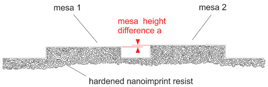
Figure 613.
Schematic to visualize the vertical resolution limits in 3D nanoimprint lithography defining mesa structures of different heights. The resist is depicted via schematic organic molecules. The size relations are not to scale: vertical mesa height difference of a = 0.2 nm to 1 nm, lateral mesa width of 6 to 40 µm, and vertical mesa heights 10 to 300 nm. The dotted line is drawn to guide the eye to visualize a 3D surface structure.