Boron-doped diamond (BDD) acts as an excellent p-type conductive material for high-temperature, high-power and radiation-proof photoelectronic devices with its large band gap at room temperature (5.47 eV) and high thermal conductivity.
- diamond-based
- one-dimensional metal oxide
- heterojunction
- high temperature
1. Introduction
Metal oxide materials have attracted great attention from the scientific community because of their important technical applications. One-dimensional (1D) nanorods (NRs), nanowires (NWs) and nanotubes (NTs) formed from metal oxides (such as ZnO, TiO2 and WO3) enable fabrication of some specific nanodevices for optoelectronic applications, for instance, photodetectors [1[1][2],2], light-emitting diodes (LED) [3], and solar cells [4,5][3]. This is because of the large surface-area-to-volume ratio, excellent charge carrier transport performance and good crystallization ability shown by these types of nanostructures [6,7][6][7]. Thus far, heterostructure optoelectronic devices have been formed by depositing n-type metal oxides on various p-type substrates, including Si [8,9[8][9][10][11],10,11], GaN [12,13,14][12][13][14], NiO [15], Cu2O [16,17,18[16][17][18][19],19], graphene [20[20][21],21], boron-doped diamond (BDD) film [22,23[22][23][24][25][26][27],24,25,26,27], and organic material [28]. Among them, BDD acts as an excellent p-type conductive material for high-temperature, high-power and radiation-proof photoelectronic devices with its large band gap at room temperature (5.47 eV) and high thermal conductivity [29]. When combining 1D metal oxide with p-type diamond, one has to explore the carrier transport behavior of the formed heterojunction devices, which has both theoretical and application importance for designing new photoelectronic devices for extremely harsh environments, such as outer space or nuclear energetics industries. In recent years, p-type BDD has been used in combination with various 1D-structured metal oxides (for instance ZnO [22,30,31[29][30][31][32][33],32,33], WO3 [34][35][36] [34,35,36] and TiO2 [37,38,39,40,41][37][38][39][40][41]) to form heterojunctions demonstrating effects of rectification and negative differential resistance (NDR), which may be widely used in various technologies. However, no comprehensive discussion focusing specifically on electrical characteristic of diamond-based p-n heterojunctions has been published.
2. Heterojunctions with 1D Metal Oxides Semiconductors
Since the discovery of carbon NTs by Professor Iijima in 1991 [42], 1D nanomaterials have quickly become one of the hotspots in the research of nanomaterials and functional devices. Carbon NTs have excellent physical and chemical properties, such as large surface-area-to-volume ratio, high mechanical strength and brilliant thermal conductivity, as well as good chemical stability. However, the use of presently existing growth technologies does not allow a readily available effective chiral control over the synthesis of carbon NTs [43], always resulting in a compound with both metallic and semiconducting properties. As such, it is impossible to obtain a completely pure semiconductor, which greatly limits the applications of optoelectronic devices.
Because of the above limitation, researchers started with the development and investigation of other 1D semiconductor nanomaterials. Silicon (Si) is the most widely used semiconductor material for optoelectronics devices. Professor Charles Lieber of Harvard University, as the leading expert in this field, for the first time has successfully prepared Si NWs [44] [44] and employed them in photovoltaic sub-devices, biosensors, etc. [45[45][46],46], showing the revealed nanomaterials and devices to have broad-range expectations in engineering.
However, Si NWs also demonstrate some shortcomings, such as easy oxidation to form polycrystalline or crystal defects in air, which may have a prevailing effect on the electrical transmission characteristic. Due to this fact, researchers reoriented to the development and implementation of 1D nanometer semiconducting materials with less oxidizing ability and higher stability. In 2001, the discovery of metal oxide semiconductor nanobelts pushed the study of nanomaterials forward to a new challenge. Metal oxides as the prime candidates for new functional inorganic materials are finding many promising applications in aerospace, biological engineering, semiconductor electronics, functional ceramics, and other fields. The 1D metal oxide nanosystems belong to the most prominent examined systems due to their good crystal quality, low defect density, excellent charge-carrier mobility, and fast response [47], thereby forming a promising replacement for traditional silicon-based electronic and optical devices.
The most recent studies have reported on the excellent optical–electronic performance of 1D metal oxides as well as new functional devices based on various substrate materials. Du et al. prepared a high-speed ultraviolet photoelectricity detector of ZnO-NWs Schottky barrier based on the surface-ionic-gate powered by tribo-nanometer generator [48]. Wang et al. demonstrated a novel bipolar response in self-powered ZnO NWs/Sb2Se3 heterojunction photodetector with adjustable polarity switching wavelength. As demonstrated in Figure 1, the output signal shows the change in the photocurrent polarity between shorter (405 nm–690 nm) and longer (760 nm–880 nm) wavelength regions [49]. Gao et al. have recently obtained a UV-free white LED based on high-level Fe-doped p-ZnO NWs arrays on the n-GaN substrate [12]. Peng et al. developed a real-time wearable UV-radiation monitor by exploiting the excellent properties of p-CuZnS/n-TiO2 photodetector [50]. Tang et al. proposed a feasible way to improve the hole doping in ZnO:N films with introduced beryllium and demonstrated strong near-band edge UV emission of the ZnO homojunction LED devices, which can be observed even at 400 K under continuous current injection [51]. Ye et al. improved the performance of n-ZnO NRs/p-GaN LED with the use of transparent graphene electrode. The transparent graphene electrode was used as the current diffusion layer, showing better performance compared to that in the ITO analogs [52]. The photoelectrochemical self-powered photodetectors related to ZnO/CdS NWs were manufactured by Zhang’s group [53]. The ZnO NWs were used as the carrier collection channels and UV absorbers with a well-organized structure to efficiently absorb light, whereas CdS nanoparticles were used as the visible photosensitizers. Prepared ZnO NWs/CdS structures demonstrate superfast response time and effective sensitivity to visible light and UV in the absence of power.
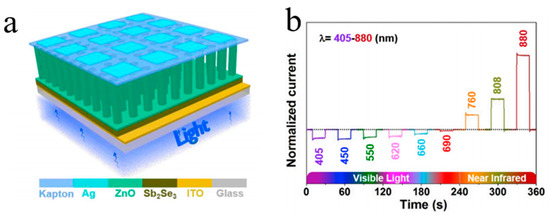
Figure 1. (a) Schematic view of the photodetector and (b) normalized photocurrent under illumination of light with different wavelengths [49].
Cheng et al. fabricated a SnS/TiO2 NTs arrays photoelectrode synthesized by anodization combined with electrodeposition technique, which was used to degrade 2,4,6-trichlorophenol under simulated visible light irradiation [54]. Yan et al. prepared photocatalytic binary composite MoS2/TiO2 (NTs) heterojunction (Figure 2). The composite material has demonstrated good photocatalytic disinfection effect and recyclability and as such has a broad field of potential applications in water disinfection [55]. Gu et al. reported on the preparation of novel WO3 NRs/graphene/BiV1−xMoxO4 heterojunction photoelectrode for photoelectrochemical water splitting. The heterojunction exhibits an enhanced photocurrent density, which makes light conversion efficiency significantly improved [56].
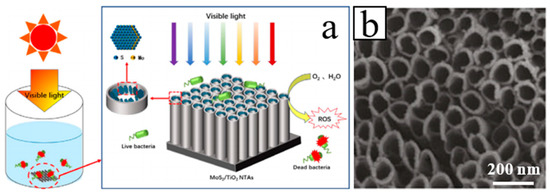
Figure 2. (a) Schematic diagram and (b) SEM image of the MoS2/TiO2 NTs fabrication process [55].
Specifically, these studies provide new strategies and insights for the fabrication of high-efficiency optoelectronic devices. One may see that most of the existing 1D metal oxide heterojunctions are generally based on Si, GaN and Cu2O, etc., and such devices show excellent photoelectric performance under normal environmental conditions. However, due to the small size of nanostructures, both light and injection current will cause a significant thermal effect. Since the thermal conductivity of the listed substrates is low, it leads to the rise in the thermal noise phenomenon and fluctuation of the effective barrier height at a high temperature. With the temperature rise, an increase in the leakage current, a drift of the threshold voltage and enhanced thermal noise degree will affect the sensitivity and reliability of the device. In addition, there is a large thermal coefficient difference between the metal oxides and the Si substrate. The interface between these two materials plays an important role in the device performance: the heterogeneity at the interface will cause the effective barrier height to fluctuate with the reduced performance of a device. This phenomenon is more evident in harsh environments such as high temperature and high flux [57,58,59][57][58][59].
3. P-Type B-Doped Diamond Films
Compared with other wide band gap semiconducting substrates (NiO2, GaN, SiC, etc.), diamond has favorable intrinsic optoelectronic performance, for instance, high thermal conductivity (22 W·cm−1·K−1), high carrier mobility (2200 and 1800 cm2·V−1·s−1), high electrical breakdown field (10 MV·cm−1) and high saturation velocity (2.7 × 10⁻⁷ cm·s−1) [60,61][60][61]. Therefore, diamond is regarded as a suitable material for high power and high temperature to cooperate with metal oxide semiconductors in optoelectronic devices. So far, the main requirements include high-quality epitaxial growth as well as doping. However, because of the contradiction between structural quality and the electrical properties of p-diamond, it is still a challenge to produce high-quality p-type diamond structures. With boron doping, diamond can be transformed from an insulator into a semiconductor or even a superconductor, wherein a boron atom is in the form of a host impurity in the diamond. High-boron doping in the diamond film may enhance its electrical resistivity (up to 10−3 Ω·cm order). In order to improve the efficiency of B-doping pursuing high mobility and high crystal quality, many efforts have been implemented.
Experimentally, Li’s group obtained the BDD film synthesized by hot filament chemical vapor deposition (HFCVD) [62]. B(OCH3)3 was utilized as the boron doping source in a methane (CH4) and hydrogen (H2) reaction atmosphere with a flow rate of 0, 2, 5, 10 and 20 sccm. The resistances decrease for the B-doping diamond films grew with increasing the H2 flow rate tested by Hall-effect measurement. The undoped diamond film consists of pyramid-shaped grains. With the increase of the B-flow rate up to 2 sccm and 10 sccm, the majority of grains showed lamellar-shaped twin characteristic, on account of the renucleation induced by B-doping. As for 20 sccm, the grains showed a dominating pyramid-shaped morphology, and a twinned crystal appeared (Figure 3). Raman spectroscopy (Figure 4) is an effective technique to investigate the structure of doped diamond. It is worth noting that owing to the high content of BDD, the p-degenerated diamond peak (1332 cm−1) shows an asymmetric curve and shifts towards the lower wavelength values in the region-centered phonon bands. Moreover, two wide bands that appear at 500 cm−1 and 1200 cm−1 in the low-frequency spectrum portion are consistent with two maximum values of phonon density in the diamond state.
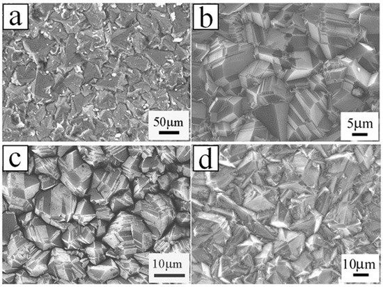
Figure 3. SEM images of the boron-doped diamond (BDD) with plane view grown with the boron of (a) 2 sccm, (b) 2 sccm, (c) 10 sccm and (d) 20 sccm [62].
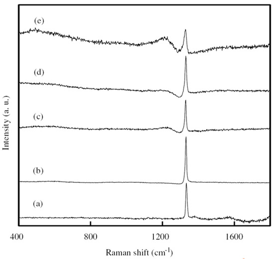
Figure 4. Raman pattern of BDD grown with the boron of (a) 0 sccm, (b) 2 sccm, (c) 5 sccm, (d) 10 sccm and (e) 20 sccm [62].
In the most recent study [63], a small amount of sulfur was added during the deposition of BDD films by microwave plasma chemical vapor deposition (MPCVD), as reported by Liu’s group. The results show the highest values of at once doping efficiency, growth rate, hole mobility and concentration, crystal mass and surface morphology of boron attained with the addition of sulfur (Figure 5). In the presence of an appropriate amount of sulfur, a high carrier concentration of 1.2 × 10¹⁹ at/cm3 may be obtained during the growth process when the B-C ratio is only 2.5 ppm, which denotes a high efficiency of boron doping. The regulation mechanism of sulfur addition has been considered in terms of sulfur-induced plasma changes and possible boron-sulfur complex formation.
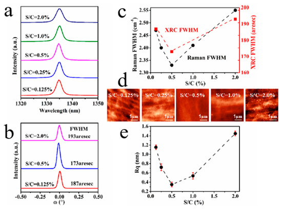
Figure 5. Boron/sulfur co-doped diamond thin films with the different S/C gas proportion: (a) Raman pattern. (b) X-ray rocking curves (XRCs). (c) Full width at half maximum of the Raman pattern and XRCs. (d) Atomic force microscopy (AFM) image (5 × 5 μm2). (e) Root mean square (RMS) surface roughness (Rq) [63].
Wei et al. [64] reported on the B-doped double-layer diamond films fabricated by MPCVD and discussed the influence of B-doping concentrations on the surface morphology, crystal quality, surface composition, conductivity and secondary electron emission properties. With increasing boron doping amount, the conductivity becomes beneficial to the emission of secondary electrons. However, as a consequence of the declining quality of the diamond crystals (Figure 6), the increased sp2 carbon on the surface and the boron segregation on the surface will reduce the effects of secondary electron emission in the films. Therefore, this improves vertical conductance, which increases the escape depth of secondary electrons and obviously leads to the reduced surface performance with the B doping. The results show that the films with the boron-doped layer demonstrate a low concentration of the crystals with excellent quality and sufficient conductivity, which helps to attain the outstanding properties of the secondary electron emission.
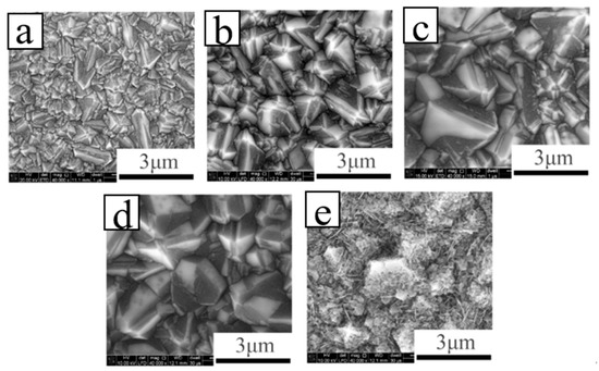
Figure 6. SEM images of BDD films grown with flow rate: (a) B 0 sccm, (b) B 0.5 sccm, (c) B 1 sccm, (d) B 2 sccm, (e) B 5 sccm [64].
Specifically, the discussed results referring to BDD demonstrate strategies for improving the doping efficiency, hole mobility, carrier concentrations, conductivity and the diamond crystal quality to further provide an efficient way to grow high-quality p-diamond material, restoring its lattice mismatch and demonstrating potential for p-BDD-based applications in optoelectronics.
References
- Wang, W.; Qi, J.; Wang, Q.; Huang, Y.; Liao, Q.; Zhang, Y. Single ZnO nanotetrapod-based sensors for monitoring localized UV irradiation. Nanoscale 2013, 5, 5981–5985. [Google Scholar] [CrossRef]
- Huo, N.; Yang, S.; Wei, Z.; Li, J. Synthesis of WO3 nanostructures and their ultraviolet photoresponse properties. J. Mater. Chem. C 2013, 1, 3999–4007. [Google Scholar] [CrossRef]
- Zhang, X.; Lu, M.; Zhang, Y.; Chen, L.; Wang, Z. Fabrication of a high-brightness blue-light-emitting diode using a ZnO-Nanowire array grown on p-GaN thin film. Adv. Mater. 2009, 21, 2767–2770. [Google Scholar] [CrossRef]
- Jean, J.; Chang, S.; Brown, P.R.; Cheng, J.J.; Rekemeyer, P.H.; Bawendi, M.G.; Gradecak, S.; Bulovic, V. ZnO nanowire arrays for enhanced photocurrent in PbS quantum dot solar cells. Adv. Mater. 2013, 25, 2790–2796. [Google Scholar] [CrossRef] [PubMed]
- Zhang, Y.; Wang, L.; Liu, B.; Zhai, J.; Fan, H.; Wang, D.; Lin, Y.; Xie, T. Synthesis of Zn-doped TiO2 microspheres with enhanced photovoltaic performance and application for dye-sensitized solar cells. Electrochim. Acta 2011, 56, 6517–6523. [Google Scholar] [CrossRef]
- Chai, G.; Lupan, O.; Chow, L.; Heinrich, H. Crossed zinc oxide nanorods for ultraviolet radiation detection. Sens. Actuators A Phys. 2009, 150, 184–187. [Google Scholar] [CrossRef]
- Wu, P.M.; Ishii, S.; Tanabe, K.; Munakata, K.; Hammond, R.H.; Tokiwa, K.; Geballe, T.H.; Beasley, M.R. Synthesis and ionic liquid gating of hexagonal WO3 thin films. Appl. Phys. Lett. 2015, 106, 042602. [Google Scholar] [CrossRef]
- Chebil, W.; Gokarna, A.; Fouzri, A.; Hamdaoui, N.; Nomenyo, K.; Lerondel, G. Study of the growth time effect on the structural, morphological and electrical characteristics of ZnO/p-Si heterojunction diodes grown by sol-gel assisted chemical bath deposition method. J. Alloys Compd. 2019, 771, 448–455. [Google Scholar] [CrossRef]
- Ko, K.B.; Ryu, B.D.; Han, M.; Hong, C.H.; Doan, T.A.; Cuong, T.V. Inserting dome shape microstructure for enhancement of ultraviolet photodetector performance of n-ZnO nanorods/p-Si heterojunction. J. Alloys Compd. 2020, 823, 153884. [Google Scholar] [CrossRef]
- Rahman, M.A.; Scott, J.A.; Gentle, A.; Phillips, M.R.; Ton-That, C. A facile method for bright, colour-tunable light-emitting diodes based on Ga-doped ZnO nanorods. Nanotechnology 2018, 29, 425707. [Google Scholar] [CrossRef]
- Li, L.; Zhang, Y.; Wang, R.; Sun, J.; Si, Y.; Wang, H.; Pan, C.; Dai, Y. Ferroelectricity-induced performance enhancement of V-doped ZnO/Si photodetector by direct energy band modulation. Nano Energy 2019, 65, 104046. [Google Scholar] [CrossRef]
- Li, H.; Zhao, W.; Liu, Y.; Liang, Y.; Ma, L.; Zhu, M.; Yi, C.; Xiong, L.; Gao, Y. High-level-Fe-doped p-type ZnO nanowire array/n-GaN film for ultraviolet-free white light-emitting diodes. Mater. Lett. 2019, 239, 45–47. [Google Scholar] [CrossRef]
- Khan, F.; Khan, W.; Kim, S.D. High-Performance Ultraviolet Light Detection Using nano-scale-fin isolation AlGaN/GaN heterostructures with ZnO nanorods. Nanomaterials 2019, 9, 440. [Google Scholar] [CrossRef] [PubMed]
- Jeong, J.; Choi, J.E.; Kim, Y.J.; Hwang, S.; Kim, S.K.; Kim, J.K.; Jeong, H.Y.; Hong, Y.J. Reverse-bias-driven dichromatic electroluminescence of n-ZnO wire arrays/p-GaN film heterojunction light-emitting diodes. Appl. Phys. Lett. 2016, 109, 101103. [Google Scholar] [CrossRef]
- Li, Y.; Wan, C.; Chang, C.; Tsai, W.; Huang, Y.; Wang, K.; Yang, P.; Cheng, H. Thickness effect of NiO on the performance of ultraviolet sensors with p-NiO/n-ZnO nanowire heterojunction structure. Vacuum 2015, 118, 48–54. [Google Scholar] [CrossRef]
- Fu, K.; Huang, J.; Yao, N.; Deng, X.; Xu, X.; Li, L. Hybrid nanostructures of TiO2 nanorod array/Cu2O with a CH3NH3PbI3 interlayer for enhanced photocatalytic activity and photoelectrochemical performance. RSC Adv. 2016, 6, S7695–S7700. [Google Scholar] [CrossRef]
- Perng, D.; Lin, H.; Hong, M. High-performance ultraviolet detection and visible-blind photodetector based on Cu2O/ZnO nanorods with poly-(N-vinylcarbazole) intermediate layer. Appl. Phys. Lett. 2015, 107, 241113. [Google Scholar] [CrossRef]
- Wang, W.; Wu, Z.; Eftekhari, E.; Huo, Z.; Li, X.; Tade, M.O.; Yan, C.; Yan, Z.; Li, C.; Li, Q.; et al. High performance heterojunction photocatalytic membranes formed by embedding Cu2O and TiO2 nanowires in reduced graphene oxide. Catal. Sci. Technol. 2018, 8, 1704–1711. [Google Scholar] [CrossRef]
- El-Shaer, A.; Ismail, I.W.; Abdelfatah, M. Towards low cost fabrication of inorganic white light emitting diode based on electrodeposited Cu2O thin film/TiO2 nanorods heterojunction. Mater. Res. Bull. 2019, 116, 111–116. [Google Scholar] [CrossRef]
- Kwon, Y.; Kang, S.O.; Cheon, J.A.; Song, Y.; Lee, J.J. Fabrication of a Graphene/ZnO based p-n junction device and its ultraviolet photoresponse properties. Appl. Surf. Sci. 2017, 415, 2–7. [Google Scholar] [CrossRef]
- Weng, B.; Wu, J.; Zhang, N.; Xu, Y. Observing the role of graphene in boosting the Two-electron reduction of oxygen in graphene-WO3 nanorod photocatalysts. Langmuir 2014, 30, 5574–5584. [Google Scholar] [CrossRef] [PubMed]
- Sang, D.; Li, H.; Cheng, S.; Wang, Q.; Liu, J.; Wang, Q.; Wang, S.; Han, C.; Chen, K.; Pan, Y. Ultraviolet photoelectrical properties of a n-ZnO nanorods/p-diamond heterojunction. RSC Adv. 2015, 5, 49211–49215. [Google Scholar] [CrossRef]
- Li, H.; Sang, D.; Cheng, S.; Lu, J.; Zhai, X.; Chen, L.; Pei, X. Epitaxial growth of ZnO nanorods on diamond and negative differential resistance of n-ZnO nanorod/p-diamond heterojunction. Appl. Surf. Sci. 2013, 280, 201–206. [Google Scholar] [CrossRef]
- Sang, D.; Li, H.; Cheng, S.; Wang, Q.; Yu, Q.; Yang, Y. Electrical transport behavior of n-ZnO nanorods/p-diamond heterojunction device at higher temperatures. J. Appl. Phys. 2012, 112, 036101. [Google Scholar] [CrossRef]
- Davydova, M.; Laposa, A.; Smarhak, J.; Kromka, A.; Neykova, N.; Nahlik, J.; Kroutil, J.; Drahokoupil, J.; Voves, J. Gas-sensing behaviour of ZnO/diamond nanostructures. Beilstein J. Nanotechnol. 2018, 9, 22–29. [Google Scholar] [CrossRef] [PubMed]
- Han, Y.; Zhang, L.; Wang, Y.; Zhang, H.; Zhang, S. Photoelectrocatalytic activity of an ordered and vertically aligned TiO2 nanorod array/BDD heterojunction electrode. Sci. Bull. 2017, 62, 619–625. [Google Scholar] [CrossRef]
- Suzuki, N.; Okazaki, A.; Kuriyama, H.; Serizawa, I.; Hirami, Y.; Hara, A.; Hirano, Y.; Nakabayashi, Y.; Roy, N.; Terashima, C.; et al. Synergetic effect in water treatment with mesoporous TiO2/BDD Hybrid electrode. RSC Adv. 2020, 10, 1793–1798. [Google Scholar] [CrossRef]
- Ranjith, K.S.; Kumar, R.T.R. Facile construction of vertically aligned ZnO nanorod/PEDOT: PSS hybrid heterojunction-based ultraviolet light sensors: Efficient performance and mechanism. Nanotechnology 2016, 27, 095304. [Google Scholar] [CrossRef]
- Li, H.; Cheng, S.; Li, J.; Song, J. A Review on the low-dimensional and hybridized nanostructured diamond films. J. Nanomater. 2015, 2015, 692562. [Google Scholar] [CrossRef]
- Sang, D.; Wang, Q.; Wang, Q.; Zhang, D.; Hu, H.; Wang, W.; Zhang, B.; Fan, Q.; Li, H. Improved electrical transport properties of an n-ZnO nanowire/p-diamond heterojunction. RSC Adv. 2018, 8, 28804–28809. [Google Scholar] [CrossRef]
- Sang, D.; Liu, J.; Wang, X.; Zhang, D.; Ke, F.; Hu, H.; Wang, W.; Zhang, B.; Li, H.; Liu, B.; et al. Negative differential resistance of n-ZnO nanorods/p-degenerated diamond heterojunction at high temperatures. Front. Chem. 2020, 8, 531. [Google Scholar] [CrossRef] [PubMed]
- Saravanan, A.; Huang, B.R.; Chu, J.P.; Prasannan, A.; Tsai, H.C. Interface engineering of ultrananocrystalline diamond/MoS2-ZnO heterostructures and its highly enhanced hydrogen gas sensing properties. Sens. Actuators B Chem. 2019, 292, 70–79. [Google Scholar] [CrossRef]
- Yu, Q.; Li, J.; Li, H.; Wang, Q.; Cheng, S.; Li, L. Fabrication, structure, and photocatalytic activities of boron-doped ZnO nanorods hydrothermally grown on CVD diamond film. Chem. Phys. Lett. 2012, 539, 74–78. [Google Scholar] [CrossRef]
- Wang, L.; Cheng, S.; Wu, C.; Pei, K.; Song, Y.P.; Li, H.; Wang, Q.; Sang, D. Fabrication and high temperature electronic behaviors of n-WO3 nanorods/p-diamond heterojunction. Appl. Phys. Lett. 2017, 110, 052106. [Google Scholar] [CrossRef]
- Yin, Z.; Tordjman, M.; Vardi, A.; Kalish, R.; Del Alamo, J.A. Diamond:H/WO3 metal–oxide–semiconductor field-effect transistor. IEEE Electr. Device L 2018, 39, 540–543. [Google Scholar] [CrossRef]
- Tordjman, M.; Weinfeld, K.; Kalish, R. Boosting surface charge-transfer doping efficiency and robustness of diamond with WO3 and ReO3. Appl. Phys. Lett. 2017, 111, 111601. [Google Scholar] [CrossRef]
- Suzuki, N.; Okazaki, A.; Kuriyama, H.; Serizawa, I.; Hara, A.; Hirano, Y.; Nakabayashi, Y.; Roy, N.; Terashima, C.; Nakata, K.; et al. Synthesis of mesoporous TiO2/boron-doped diamond photocatalyst and its photocatalytic activity under deep UV Light (λ= 222 nm) irradiation. Molecules 2018, 23, 3095. [Google Scholar] [CrossRef] [PubMed]
- Yuan, J.; Li, H.; Gao, S.; Lin, Y.; Li, H. A facile route to n-type TiO2-nanotube/p-type boron-doped-diamond heterojunction for highly efficient photocatalysts. Chem. Commun. 2010, 46, 3119–3121. [Google Scholar] [CrossRef]
- Yuan, J.; Li, H.; Wang, Q.; Cheng, S.; Zhang, X.; Yu, H.; Zhu, X.; Xie, Y. Fabrication, Characterization and optical properties of TiO2 nanotube arrays on boron-doped diamond film through liquid phase deposition. Chem. Res. Chin. Univ. 2014, 30, 18–22. [Google Scholar] [CrossRef]
- Liu, Z.; Zhao, D.; Min, T.; Wang, H. 3D TiO2/Diamond ultraviolet detector using back-to-back Pd schottky electrode. Phys. Status Solidi A 2020, 217, 2000218. [Google Scholar] [CrossRef]
- Behul, M.; Vojs, M.; Marton, M.; Michniak, P.; Mikolasek, M.; Kurniawan, M.; Honig, H.L.; Zyabkin, D.V.; Ramirez, M.O.; Spiess, L.; et al. Nanostructured boron doped diamond enhancing the photoelectrochemical performance of TiO2/BDD heterojunction anodes. Vacuum 2020, 117, 109006. [Google Scholar] [CrossRef]
- Iijima, S. Helical microtubules of graphitic carbon. Nature 1991, 354, 56–58. [Google Scholar] [CrossRef]
- Pan, Z.; Wang, Z.; Dai, Z. Nanobelts of semiconducting oxides. Science 2001, 291, 1947–1949. [Google Scholar] [CrossRef]
- Morales, A.M.; Lieber, C.M. A laser ablation method for the synthesis of crystalline semiconductor nanowires. Science 1998, 279, 208–211. [Google Scholar] [CrossRef]
- Cui, Y.; Lieber, C.M. Functional nanoscale electronic devices assembled using silicon nanowire building blocks. Science 2001, 291, 851–853. [Google Scholar] [CrossRef] [PubMed]
- Tian, B.; Kempa, T.J.; Lieber, C.M. Single nanowire photovoltaics. Chem. Soc. Rev. 2009, 38, 16–24. [Google Scholar] [CrossRef] [PubMed]
- Rasch, F.; Postica, V.; Schutt, F.; Mishra, Y.K.; Nia, A.S.; Lohe, M.R.; Feng, X.L.; Adelung, R.; Lupan, O. Highly selective and ultra-low power consumption metal oxide based hydrogen gas sensor employing graphene oxide as molecular sieve. Sens. Actuators B Chem. 2020, 320, 128363. [Google Scholar] [CrossRef]
- Yang, F.; Zheng, M.; Zhao, L.; Guo, J.; Zhang, B.; Gu, G.; Cheng, G.; Du, Z. The high-speed ultraviolet photodetector of ZnO nanowire Schottky barrier based on the triboelectric-nanogenerator-powered surface-ionic-gate. Nano Energy 2019, 60, 680–688. [Google Scholar] [CrossRef]
- Ouyang, B.S.; Zhao, H.; Wang, Z.; Yang, Y. Dual-polarity response in self-powered ZnO NWs/Sb2Se3 film heterojunction photodetector array for optical communication. Nano Energy 2020, 68, 104312. [Google Scholar] [CrossRef]
- Xu, X.; Chen, J.; Cai, S.; Long, Z.; Zhang, Y.; Su, L.; He, S.; Tang, C.; Liu, P.; Peng, H.; et al. Real-Time Wearable UV-Radiation monitor based on a high-performance p-CuZnS/n-TiO2 photodetector. Adv. Mater. 2018, 30, 1803165. [Google Scholar] [CrossRef]
- Chen, A.; Zhu, H.; Wu, Y.; Chen, M.; Zhu, Y.; Gui, X.; Tang, Z. Beryllium-Assisted p-Type doping for ZnO homojunction light-emitting devices. Adv. Funct. Mater. 2016, 26, 3696–3702. [Google Scholar] [CrossRef]
- Chen, D.; Chen, S.; Yue, S.; Lu, B.; Pan, X.; He, H.; Ye, Z. N-ZnO nanorod arrays/p-GaN light-emitting diodes with graphene transparent electrode. J. Lumin. 2019, 216, 116719. [Google Scholar] [CrossRef]
- Bai, Z.; Fu, M.; Zhang, Y. Vertically aligned and ordered ZnO/CdS nanowire arrays for self-powered UV-visible photosensing. J. Mater. Sci. 2017, 52, 1308–1317. [Google Scholar] [CrossRef]
- Zhang, X.; Gao, Y.; Nengzi, L.; Li, B.; Gou, J.; Cheng, X. Synthesis of SnS/TiO2 nano-tube arrays photoelectrode and its high photoelectrocatalytic performance for elimination of 2,4,6-trichlorophenol. Sep. Purif. Technol. 2019, 228, 115742. [Google Scholar] [CrossRef]
- Yan, H.; Liu, L.; Wang, R.; Zhu, W.; Ren, X.; Luo, L.; Zhang, X.; Luo, S.; Ai, X.; Wang, J. Binary composite MoS2/TiO2 nanotube arrays as a recyclable and efficient photocatalyst for solar water disinfection. Chem. Eng. J. 2020, 401, 126052. [Google Scholar] [CrossRef]
- Gu, M.; Zhang, H.; Ji, J.; Pei, X. Fabrication of WO3 nanorod/graphene/BiV1−xMoxO4 heterojunction photoelectrode for efficient photoelectrochemical water splitting. J. Mater. Sci. Mater. Electron. 2020, 31, 3323–3331. [Google Scholar] [CrossRef]
- Das, A.; Kushwaha, A.; Sivasayan, R.K.; Chakraborty, S.; Dutta, H.S.; Karmakar, A.; Chattopadhyay, S.; Chi, D.Z.; Dalapati, G.K. Temperature-dependent electrical characteristics of CBD/CBD grown n-ZnO nanowire/p-Si heterojunction diodes. J. Phys. D Appl. Phys. 2016, 49, 145105. [Google Scholar] [CrossRef]
- Singh, S.K.; Hazra, P. Performance of RF sputtered p-Si/n-ZnO nanoparticle thin film heterojunction diodes in high temperature environment. Appl. Surf. Sci. 2016, 400, 206–211. [Google Scholar] [CrossRef]
- Makhlouf, M.M.; El-Nahass, M.M.; Zeyada, M.H. Fabrication, temperature dependent current-voltage characteristics and photoresponse properties of Au/α-PbO2/p-Si/Al heterojunction photodiode. Mater. Sci. Semicond. Process. 2017, 58, 68–75. [Google Scholar] [CrossRef]
- Angus, J.C.; Hayman, C.C. Low-Pressure, Metastable growth of diamond and “diamondlike” phases. Science 1988, 241, 913–921. [Google Scholar] [CrossRef]
- Reggiani, L.; Bosi, S.; Canali, C.; Nava, F.; Kozlov, S.F. Hole-drift velocity in natural diamond. Phys. Rev. B 1981, 23, 3050–3057. [Google Scholar] [CrossRef]
- Li, H.; Zhang, T.; Li, L.; Lu, X.; Li, B.; Jin, Z.; Zou, G. Investigation on crystalline structure, boron distribution, and residual stresses in freestanding boron-doped CVD diamond films. J. Cryst. Growth 2010, 312, 1986–1991. [Google Scholar] [CrossRef]
- Liu, D.; Hao, L.; Chen, Z.; Zhao, W.; Shen, Y.; Bian, Y.; Tang, K.; Ye, J.; Zhu, S.; Zhang, R.; et al. Sulfur regulation of boron doping and growth behavior for high-quality diamond in microwave plasma chemical vapor deposition. Appl. Phys. Lett. 2020, 117, 022101. [Google Scholar] [CrossRef]
- Wei, K.; Wang, R.; Li, J.; Liu, B.; Wei, Q.; Wu, R.; Wu, S.; Hu, W.; Wang, H. Secondary electron emission properties of double-layer B-doped diamond films. Diam. Relat. Mater. 2020, 106, 107826. [Google Scholar] [CrossRef]
