As the need for green and effective utilization of energy continues to grow, the advancements in the energy and power electronics industry are constantly driven by this need, as both industries are intertwined for obvious reasons. The developments in the power electronics industry has over the years hinged on the progress of the semiconductor device industry. The semiconductor device industry could be said to be on the edge of a turn into a new era, a paradigm shift from the conventional silicon devices to the wide band gap semiconductor technologies. While a lot of work is being done in research and manufacturing sectors, it is important to look back at the past, evaluate the current progress and look at the prospects of the future of this industry. This paper is unique at this time because it seeks to give a good summary of the past, the state-of-the-art, and highlight the opportunities for future improvements. A more or less ‘forgotten’ power electronic switch, the four-quadrant switch, is highlighted as an opportunity waiting to be exploited as this switch presents a potential for achieving an ideal switch.
- bipolar transistors,insulated gate bipolar transistors,power semiconductor devices
1. Introduction
In spite of the decreasing world population growth rate over the years, the human population on planet earth has continued to grow reaching just under eight (8) billion people so far[1][2][3]. This growing population coupled with a drastic increase in industrialization on a massive scale has brought about huge demands for energy. The international energy agency (IEA) projects a 25% increase in the global primary energy demand between the years 2017 and 2040. It is also predicted that if no further improvements occur in the energy efficiency of the world, it could lead to a 50% increase in energy demands[4].
This rather radical increase in energy demand alongside the damaging effects of climate change and degradation of planet earth has resulted in an aggressive exploitation of non-renewable and pollutant sources of energy over the years. To combat the detrimental effects of man’s long-standing pollution of the environment and attempt to attain a state of balance and environmental purity on planet earth, there has been a rise in the utilization of renewable energy sources. Although the supply of energy from renewable energy sources to the energy supply mix continues to grow, in order to reach this state of balance and purity in the energy cycle, there needs to be a consistent increase in the efficiency of energy generation, supply and utilization. This need defines the drive of the power, energy and electronics industry and thus the drive of the power electronics industry[5][6][7].
The progress of the power electronics industry has been contingent on the level of progress in the semiconductor power device industry, otherwise known as the power electronic device industry and this particularly on the advancements in power electronic switches[8]. The power electronic switch industry has grown and improved drastically over the years and is now in a transitional phase from the more common silicon semiconductor technologies to a totally new phase of wide band gap (WBG) technologies[9][10][11][12][13][14][15][16]. This new phase is characterized by an improvement in the various characteristics and manufacturing techniques already in place for power electronic switches[17][18][19][20][21][22][23][24][25][26]. Generally speaking, advancements in power electronic switches are primarily to increase the switching speed, that is to reduce the time it takes for the switch to turn-on and turn-off, and to increase the power the switch is capable of handling[27][28].
2. Classification of Power Electronic Switches
Modern power electronic devices can be classified in a number of ways based on the number of terminals, the number of pn junctions, level of controllability, bidirectional capability, and the gate signal requirements to name just a few. In Figure 2, the more prominent classification of the modern power electronic devices is presented.
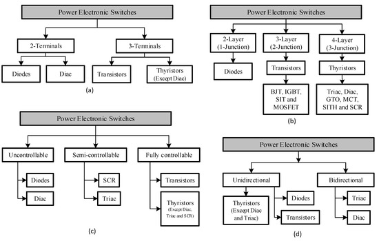
Figure 2. Classification of modern power electronic switches based on (a) number of terminals, (b) number of layers or junctions, (c) controllability and (d) bidirectional capability.
Taking the number of terminals, power electronic devices are broadly divided into two groups, the 2-terminal and the 3-terminal devices. The two terminal devices are devices whose switch state solely depends on the circuits which they are externally connected to. The diode and the diac are prime examples and occupants of the 2-terminal device category. As it can be observed in Figure 2a, the 3-terminal device consists of the thyristor and the transistor. These are devices whose switching state does not solely depend on the external circuit to which they are connected but also depends on the driving signal at their respective gates.
In Figure 2b, the classification of modern power electronic switches based on their number of junctions or layers is presented. This classification could be one of the most appropriate and robust classification of semiconductor switching devices. Based on this classification, there are three categories, namely: the 1-juntion or 2-layer, the 2-juntion or 3-layer and the last one which is a 3-junction or 4-layer group of power electronic switches.
The 1-juntion or 2-layer group consists of the diode, the 2-junction or 3-layer group consists of the transistor and the 3-junction or 4-layer group consists of the thyristor families of power electronic devices. This classification was earlier referred to as the most robust because all of the different families find themselves in their respective family-groups and it speaks more to their structure than to just their characteristics.
A third classification of the power electronic switches is based on their controllability. In this classification, there are three groups, the uncontrollable switches, semi-controllable switches, and the fully controllable switches. The uncontrollable switches consist of the diode and the diac just like in the 2-terminal classification based on their number of terminals. These switches are in this class because the turn-on and turn-off cannot be controlled and is solely determined by the external power circuit. The semi-controllable switches can be turned on but cannot be turned off directly from the gate. In this category, the thyristor, specifically the silicon-controlled rectifier (SCR) and the triac are prime members. As can be seen in Figure 2c, the last group, the BJT, MOSFET, GTO, static induction thyristor (SITH), static induction transistor (SIT), IGBT and MOS-controlled thyristor (MCT) are all members.
The fourth main classification is based on their bidirectional or unidirectional current capability; this is presented in Figure 2d. It is seen that only the triac, diac, and the RCT are capable of bidirectional current capability while the rest are only capable of unidirectional current flow. It is worthy of note that most commercially available MOSFETs have body drain diodes which are antiparallel to the MOSFET switch hence giving it a bidirectional capability but the flow of current through the body diode cannot be controlled externally.
Other classifications of power electronic switches include the gate signal requirement and the type of charge carriers utilized in the switching technology. For the gate signal requirements, some switches such as BJTs, MOSFETs, IGBTs, and SITs require a continuous gate signal to keep the switch operational, the GTO, MCT and the SCR only require a pulse gate signal while the diode does not have a gate to start with. For the charge carriers used, this classification is in two groups, the majority and the minority charge carriers. In majority carriers, only one type of charge carrier is used in the transportation of current through the semiconductor. That is, either electrons or holes in an n-type semiconductor or p-type semiconductor respectively. Examples of switches that utilize majority carriers are Schottky diodes and MOSFETs. On the other hand, minority carriers use both electrons and holes to transport current through the semiconductor material. Examples of switches utilizing minority carriers are thyristors, BJTs and IGBTs.
2.1. Diodes
3.1. Diodes
Diodes are formed from a pn junction of semiconductor material, as shown in Figure 3, they have just two terminals, the anode and the cathode[29]. A diode is an uncontrollable and unidirectional switch hence, its operation is determined by the direction of the flow of current in a circuit[30].
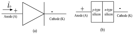
Figure 3. (a) Schematic symbol and (b) basic structure of a diode[29].
A diode is basically a short circuit when it is forward biased, that is when current is flowing from the anode to the cathode and conversely it is an open circuit when it is reverse biased, that is when the direction of the flow of current is in the opposite direction in the circuit. There are generally three types of diodes, the power diodes, schottky diode and the zener diode[31].
The power diode can be further classified into two based on their characteristics and applications. The two classes include the line-frequency diodes and the fast recovery diodes. The line frequency diodes, also known as the general-purpose diodes, are used in line frequency applications (that is frequencies around 50–60 Hz) such as in AC rectification. They are characterized by slow recovery times and can be used in applications requiring high voltage and high currents (>5 kV and kA respectively) [32].
The fast recovery diodes as their name implies are characterized by fast recovery times and are therefore utilized in high applications such as traction systems, induction heating and uninterruptible power systems (UPS). The downside with fast recovery diodes when compared to line frequency diodes is that they cannot operate at such high voltages and currents as line frequency diodes can[33].
The other types of diodes are the Schottky and Zener diodes, the schematic representation of these diodes are presented in Figure 4a,b respectively. Schottky diodes, named after Walter Schottky[34], instead of being formed from the regular pn semiconductor junction and rather formed from a metal-n semiconductor junction. The metals could be made of platinum or tungsten. This metal-n type semiconductor material junction affords the Schottky diode to have a low on-state voltage drop of as low as 0.1 V. Although its breakdown voltage is much lower than that of the power diode, it switches faster and has a high switching frequency but a higher reverse leakage current than the power diode. Due to these characteristics, Schottky diodes are often used in low voltage and high current applications like switched mode power supplies[35].
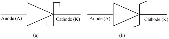
Figure 4. Schematic of (a) a schottky diode and (b) a zener diode[33].
On the other hand, a Zener diode while still being made from pn semiconductor junction, in simple terms can allow flow of current when reverse biased as long as the voltage is above a specific value known as the Zener voltage, breakdown voltage or the Zener knee voltage. The Zener diode is used to produce a stable voltage (the Zener knee voltage) from a varying supply voltage[36]. Therefore, a Zener diode can be used to generate a reference voltage for an amplifier stage or as a voltage stabilizer in low current applications. The Zener diode must be implemented with a current limiting resistor in series with itself to keep the flow of current in the Zener diode at a safe level[32].
2.2. Transistors
3.2. Transistors
When two PN junctions are combined together with the center layer of semi-conductor being common to the two outer layers, forms the transistor of either PNP or NPN type, the schematic representation and structure of BJTs is presented in Figure 5 [37]. Hence the name bipolar junction transistor (BJT), since it uses both electron and holes as charge carrier. In NPN transistor the current flows from collector to emitter, when the base is supplied with the positive voltage, while in PNP transistor the current direction is reverse i.e., from the emitter to collector when the base is supplied with a negative voltage[38]. Since, in NPN transistors, majority carriers are electrons and minority carriers are holes, the transistor is turned-on when electrons enter the base region; while in PNP transistor, majority and minority carriers are holes and electrons, respectively, thus the transistor is turned ON because of movement of holes into the base[39]. As mentioned earlier, combination of two PN-junctions, i.e., emitter-base junction and the collector-base junction with common semiconductor acting as the base, at the center, forms PNP or NPN type transistors, with the emitter, base and collector regions[40]. To achieve desired power gain, one junction is kept in forward biased while another junction is kept in reverse biased condition. The biasing type also determines the mode of operation in active mode, cut-off mode, and saturation mode. The polarity of bias junction is determined by the type of the transistor; consider PNP structure shown in Figure 5c,d[41]. For both type of transistors, emitter-base junction when in forward bias condition, due to drift, the majority carriers, either holes or electrons emitted from emitter enter the base region for recombination. Escaped remaining carriers get diffused in base region are carried forward into collector region by applying a reverse bias to the collector-base junction[42].
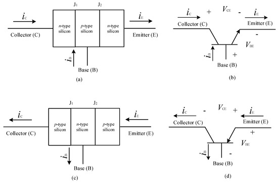
Figure 5. Structural diagram and schematic symbols of (a,b) an NPN transistor and (c,d) a PNP transistor [39].
Because of high mobility of electrons, NPN transistors have high conductivity and thus, switching time in NPN transistors is faster than that of in PNP transistors. Thus, for switching and amplification applications, NPN transistors are preferred. Collector terminal in NPN and emitter terminal in PNP transistor are supplied with positive voltage [43]. For analog applications, polysilicon emitter BJTs are used. With new technology, the size of transistors is reduced which gives high current and high-frequency gain but also increase low-frequency noise[44]. In a study by[45], it was observed that, in NPN transistors, shot noise of the base current contributes to total noise, while in a PNP transistor, generation-recombination noise adds to the total noise.
Metal oxide semiconductor field effect transistors (MOSFETs) are unipolar devices, since they have only one type of carrier, unlike BJTs. In MOSFETs, the current through the device is controlled by the voltage between its terminals, source, and gate[46] In MOSFETs, the gate is insulated from channel using silicon dioxide (SiO2) material, labelled as the deflection layer in Figure 6 [47][48]. There are two kinds of MOSFETs, as shown in Figure 6, enhancement (E) mode and depletion (D) mode, enhanced MOSFETs (EMOSFETs) also known as insulated-gate field effect transistors (IGFETs) are widely used, because of polycrystalline silicon gate materials[49].
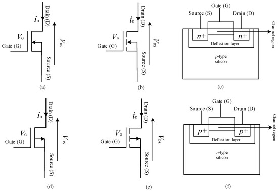
Figure 6. Diagrams showing (a) the schematic symbol of a depletion mode N-channel MOSFET, (b) the schematic symbol of an enhancement mode N-channel MOSFET (c) the structural diagram of an N-channel MOSFET (d) the schematic symbol of a depletion mode P-channel MOSFET, (e) the schematic symbol of an enhancement mode P-channel MOSFET and (f) the structural diagram of a P-channel MOSFET[48].
The structure of a depletion MOSFET (DMOSFET) is same as that of an enhancement MOSFET (EMOSFET), except in a DMOSFET, there is a narrow channel present between diffused source and drain into the substrate, adjacent to the insulated gate. N-channel and P-channel DMOSFET structures are same except for voltage polarities [50][51][52]. When an N-channel DMOSFET is operating in the depletion mode, the negative voltage on the gate repels the electrons from the channel. With an increase in gate voltage, at a certain point, the channel becomes completely depleted of electrons and channel current becomes zero. When an N-channel DMOSFET is operating in the enhancement mode, a positive voltage applied to the gate, attracts more electrons in the channel, increasing the channel conductivity[53].
EMOSFET structure does not include structural channel and only operates in enhancement mode. For an N-channel EMOSFET, when the applied gate to source voltage is positive, it attracts electrons and forms a narrow channel alongside SiO2 layer. With the increase in applied voltage; more electrons are attracted into the channel, increasing conductivity and below the threshold voltage, no channel is formed into the substrate[32]. Due to high drain to source resistance as a result of long thin lateral channel alongside insulation layer, EMOSFETs are suitable for low power applications. There are four types of EMOSFETs, the laterally diffused MOSFET (LDMOSFET), the V-groove MOSFET, the T-groove MOSFET, and the dual-gate MOSFET. The LDMOSFET structure has a shorter channel between the lightly doped source and drain[54]. It gives higher current and voltage than conventional EMOSFET and thus is suitable for high power applications. The VMOSFET structure has two source gates on top with a gate in between them and a drain at the bottom. The wide and short channel is induced between drain and source with less resistance, thus resulting in high current and power dissipation and better frequency response. The channel is formed along the V-groove between two sources and the drain, with thickness dependent upon the doping and diffusion time. In the TMOSFET structure, the source is all over top surface and drain is at the bottom, giving short vertical channel with more packing density than VMOSFET. Dual-gate MOSFETs have two gates giving low input capacitance and high-frequency applications with automatic gain control. To maintain the long-channel behavior of MOSFET, many parameters were altered during previous researches. In Brews et al., an empirical equation was proposed to find a relation between required parameters to be altered by observing long channel subthreshold behavior. The parameters considered were bias, doping level, junction depth and oxide thickness range[50][51].
The insulated gate bipolar transistor (IGBT) combines advantages of the MOSFET and a BJT, this is since it has output characteristics of a BJT and voltage control like a MOSFET[55]. The circuit symbol of IGBT is as shown in Figure 7 alongside its structural diagrams. It has three terminals, gate from MOSFET, and an emitter and collector from BJT[32]. The insulated gate has no input current and thus, IGBT can be also called as voltage controlled BJT with faster switching characteristics[31].
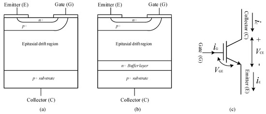
Figure 7. Diagrams showing the (a) the non-punch-through (NPT) structure of an IGBT (b) the punch-through (PT) structure of an IGBT and (c) the circuit schematic of an IGBT[55].
During operation, a parasitic transistor Qp and parasitic resistor is formed within the IGBT device because of its NPNP-like structure[55]. These parasitic elements do not affect normal operation of IGBT unless under certain conditions, like if the collector current exceeds a certain level, then the parasitic transistor Qp may turn on. When Qp is turned on, combination of Qp and Q1 output transistor creates parasitic element. This parasitic element will keep the device in always ON mode, which is known as latch up condition. It can be avoided by controlling the device operation within specified limit values[56].
The IGBT structure is formed with NPNP-like four alternating semiconductor layers creating a thyristor-like structure. Thyristor operation is disabled using deep p+ diffusion and short circuit of P-base region using emitter[55]. There are two types of IGBT structures, the symmetric and asymmetric blocking structures[57]. Symmetric blocking IGBT structure is known as non-punch-through (NPT) IGBT device since because of lightly doped N-drift region, electric field does not spread across its entire width[58]. In asymmetric IGBT also known as punch through (PT) structure as shown in Figure 7, an N-buffer layer, also called as field stop layer is introduced in the N-drift region. Unlike NPT IGBT, electric field spreads across the entire width of the N-drift region. In PT IGBT, lower forward voltage drop can be achieved by reducing thickness of N-drift region. PT IGBT operates in the first quadrant of the v-i characteristics and thus is useful in DC applications[59].
The main differences between a NPT-IGBT and a PT-IGBT is that NPT-IGBTs are more thermally stable, have a higher carrier lifetime hence resulting in a lower forward voltage drop than PT-IGBTs. NPT-IGBTs are used in AC circuits while PT-IGBTs are utilized in DC circuits[60]. Also, the temperature coefficient of the on-state voltage of NPT-IGBTs is highly positive, making the NPT-IGBTs more well suited for device paralleling since the PT-IGBTs’ temperature coefficient of the on-state voltage usually tends almost to zero [61]. PT-IGBTs are capable of switching at a higher speed with even less energy consumed during switching when compared to NPT-IGBTs of the same voltage rating[62]. However, NPT-IGBTs are manufactured through a less expensive process (diffusion process technology) than the PT-IGBTs which are made in an N-epitaxial wafer profess.
Another prominent member of the transistor family is the static induction transistor (SIT), the schematic symbol of the SIT is presented in Figure 8 [63]. The SIT was introduced in 1987, just a year before the static induction thyristor by Tokin Corporation in Japan [64]. One of the main advantages of the SIT over a field effect transistor (FET), is that the SIT structure offers advantages in obtaining higher breakdown voltages, since is not limited by the surface breakdown between gate and drain, and therefore can operate at a very high current and voltage[65][66]. The SIT is a high frequency and high power device which is described to be basically a triode vacuum tube in solid state form [67]. It is used in induction heaters, high voltage low current power supplies, linear power amplifiers, ultrasonic generators, and AM/FM transmitters[68].
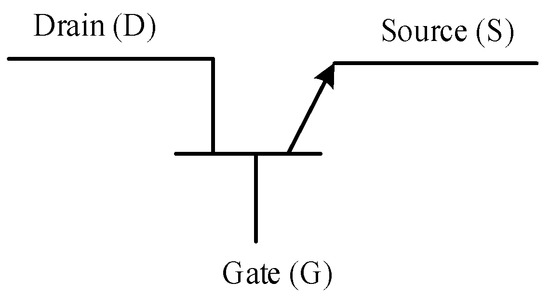
Figure 8. Schematic symbol of a static induction transistor[63].
2.3. Thyristor Families
3.3. Thyristor Families
The thyristor family of power electronic switches is as shown in Figure 9, a three terminal, four layer semiconductor device[69]. As can be seen in Figure 9, the four layers of a thyristor are made up from three alternating pn juntions. Some of the prominent members of the thyristor family includes: the SCR, GTO, static induction thyristor (SITH), MOS-controlled thyristor (MCT), triode AC switch (TRIAC) and the diode AC switch (DIAC)[70]. Thyristors are very often used to switch alternating currents and utilized when the power requirements (current and voltage) are relatively high (in excesses of a few thousand volts and amps)[71].
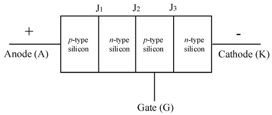
Figure 9. Basic structure of a thyristor[70].
Figure 10 shows the schematic symbol of an SCR, which is also often referred to as a thyristor as well. An SCR is a unidirectional switch just like a diode but has a gate (G) which controls its turn ON. As it has been mentioned earlier, the turn-off of a thyristor is a quite complicated process and hence a new thyristor based switch called the gate turn-off thyristor (GTO) was introduced[72]. Although the thyristor quickly gained traction in many AC applications, such as in AC drives and uninterruptible power supplies (UPSs), its turn-off incapability and the low frequency of operation (50–60 Hz) limited its application, it is alleged that the thyristor has reached saturation as far as its application is concerned[73]. In Figure 11, the schematic of a GTO is presented, it is seen to be very similar to that of the thyristor except that it can be turned-off at the gate.
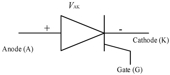
Figure 10. Schematic symbol of a silicon controlled rectifier (SCR)[70].
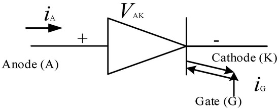
Figure 11. Schematic symbol of gate-turn-off thyristor (GTO)[72].
Again, the GTO just like the SCR is not without its unique challenges such as poor turn-off current gain and the second-breakdown problem it exhibits at turn-off. It also has a limited operating frequency of less than 5 kHz and the gate drive design is quite complex due to the need for a large reverse gate current to turn it off[74].
Another interesting power electronic device in the thyristor family is the triode AC switch also known as the triac. The schematic of a triac is presented in Figure 12a. It can be observed that a triac is simply the arrangement of two thyristors in reverse-parallel configuration in a single chip. This is more clearly depicted in Figure 12b, the gates of the two SCRs are tied together and controlled from one source[75].
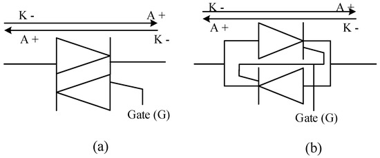
Figure 12. Schematic symbol of (a) a triode ac switch (Triac) and (b) the detailed depiction of a Triac’s formation from two SCRs[76].
Although the triac is more economical to implement than just taking two thyristors and arranging them as described in Figure 12b, its current sensitivity is worse thus having a longer turn-off time due to the minority carrier storage effects. Its frequency of operation is similar to that of a thyristor at 50–60Hz. The triac is used in solid state relays, light dimming, heating control, and some home appliances[76].
The story of the thyristor family will be incomplete without mentioning the diode AC switch otherwise known as the diac. The schematic symbol of a diac is presented in Figure 13. It is very similar to a triac except that a diac has no gate. Just like a triac, a diac has arbitrary terminal designations since it is a bilateral device. The diac is reported to find its application chiefly in switching or triggering the triac[77].
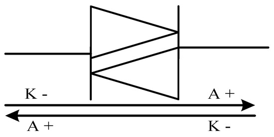
Figure 13. Schematic symbol of a diode AC switch (Diac)[77].
Other prominent members of the thyristor family include: the static induction thyristors (SITHs), MOS-controlled thyristor (MCT), reverse conducting thyristor (RCT), and the light activated-SCR (LASCR). Their respective schematic symbols are presented in Figure 14[78].
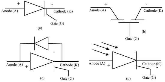
Figure 14. Schematic symbol of (a) a SITH, (b) an MCT, (c) an RCT and (d) an LASCR[78].
The SITHs were introduced around 1988 and are turned-off in a similar way to the GTO, the downside of the SITH when compared with the GTO is that it has a higher conduction drop[79][80]. It is used in induction heating applications and static var compensators. MCTs were also introduced around the same time as SITHs and also has a high gain at turn-off just like the GTO. The MCT is continuously being improved and could pose a potential threat to the IGBT as it has a smaller voltage drop and can operate in higher temperatures[75][80]. RCTs are basically achieved by the inclusion of an anti-parallel body diode across an SCR in order to achieve current flow in the opposite direction[81]. The LASCR, as their name implies are light activated and is utilized in high voltage and current systems to achieve total electrical isolation between the control and the power sections of the system[60].
References
- United Nations. “World: Total Population”, World Population Prospects 2019: Highlights. Available online: https://www.un.org/development/desa/publications/world-population-prospects-2019-highlights.html (accessed on 13 August 2020).
- United Nations Population Fund. “World Population Dashboard”. Total Population in Millions. 2020. Available online: https://www.unfpa.org/data/world-population-dashboard (accessed on 29 October 2020).
- The World Bank. “Population growth (annual %)”. World Bank Open Data. Available online: https://data.worldbank.org/indicator/SP.POP.GROW (accessed on 29 October 2020).
- IEA-International Energy Agency. World Energy Outlook 2018; IEA: Paris, France, 2018.
- Vilathgamuwa, M.; Nayanasiri, D.; Gamini, S. Power Electronics for Photovoltaic Power Systems. Synth. Lect. Power Electron. 2015, 5, 1–131.
- Bose, B.K. Global Warming: Energy, Environmental Pollution, and the Impact of Power Electronics. IEEE Ind. Electron. Mag. 2010, 4, 6–17.
- Bose, B.K. Power Electronics, Smart Grid, and Renewable Energy Systems. Proc. IEEE 2017, 105, 2011–2018.
- Mazumder, S.K. An Overview of Photonic Power Electronic Devices. IEEE Trans. Power Electron. 2016, 31, 6562–6574.
- Bindra, A. Uncovering the State of Adoption of Wide-Bandgap Power Devices. IEEE Power Electron. Mag. 2018, 5, 4–6.
- Tzou, A.-J.; Hsieh, D.-H.; Chen, S.-H.; Liao, Y.-K.; Li, Z.-Y.; Chang, C.-Y.; Kuo, H.-C. An Investigation of Carbon-Doping-Induced Current Collapse in GaN-on-Si High Electron Mobility Transistors. Electronics 2016, 5, 28.
- Dong, Y.; Son, D.-H.; Dai, Q.; Lee, J.-H.; Won, C.-H.; Kim, J.-G.; Chen, D.; Lee, J.-H.; Lu, H.; Zhang, R. High Sensitive pH Sensor Based on AlInN/GaN Heterostructure Transistor. Sensors 2018, 18, 1314.
- Gu, W.; Xu, X.; Zhang, L.; Gao, Z.; Hu, X.; Zhang, Z. Study on Neutron Irradiation-Induced Structural Defects of GaN-Based Heterostructures. Crystals 2018, 8, 198.
- Yuan, S.-H.; Chang, F.-Y.; Wuu, D.-S.; Horng, R.-H. AlGaN/GaN MOS-HEMTs with Corona-Discharge Plasma Treatment. Crystals 2017, 7, 146.
- Dogmus, E.; Kabouche, R.; Lepilliet, S.; Linge, A.; Zegaoui, M.; Ben-Ammar, H.; Chauvat, M.-P.; Ruterana, P.; Gamarra, P.; Lacam, C. InAlGaN/GaN HEMTs at Cryogenic Temperatures. Electronics 2016, 5, 31.
- Caddemi, A.; Cardillo, E.; Patanè, S.; Triolo, C. Light Exposure Effects on the DC Kink of AlGaN/GaN HEMTs. Electronics 2019, 8, 698.
- Meneghini, M.; Hilt, O.; Wuerfl, J.; Meneghesso, G. Technology and Reliability of Normally-Off GaN HEMTs with p-Type Gate. Energies 2017, 10, 153.
- Zeng, F.; An, J.; Zhou, G.; Li, W.; Wang, H.; Duan, T.; Jiang, L.; Yu, H. A Comprehensive Review of Recent Progress on GaN High Electron Mobility Transistors: Devices, Fabrication and Reliability. Electronics 2018, 7, 377.
- Chou, P.-C.; Chen, S.-H.; Hsieh, T.-E.; Cheng, S.; del Alamo, J.; Chang, E. Evaluation and Reliability Assessment of GaN-on-Si MIS-HEMT for Power Switching Applications. Energies 2017, 10, 233.
- Roccaforte, F.; Greco, G.; Fiorenza, P.; Iucolano, F. An Overview of Normally-Off GaN-Based High Electron Mobility Transistors. Materials 2019, 12, 1599.
- Millaán, J. Wide band-gap power semiconductor devices. Iet Circuits Devices Syst. 2007, 1, 372.
- Chen, R.; Li, R.; Zhou, S.; Chen, S.; Huang, J.; Wang, Z. An X-Band 40 W Power Amplifier GaN MMIC Design by Using Equivalent Output Impedance Model. Electronics 2019, 8, 99.
- Han, T.; Liu, H.; Wang, S.; Chen, S.; Li, W.; Yang, X.; Cai, M.; Yang, K. Design and Investigation of the Junction-Less TFET with Ge/Si0.3Ge0.7/Si Heterojunction and Heterogeneous Gate Dielectric. Electronics 2019, 8, 476.
- Guan, H.; Wang, S.; Chen, L.; Gao, B.; Wang, Y.; Jiang, C. Channel Characteristics of InAs/AlSb Heterojunction Epitaxy: Comparative Study on Epitaxies with Different Thickness of InAs Channel and AlSb Upper Barrier. Coatings 2019, 9, 318.
- Zhang, Z.; Guo, B.; Wang, F. Evaluation of Switching Loss Contributed by Parasitic Ringing for Fast Switching Wide Band-Gap Devices. IEEE Trans. Power Electron. 2019, 34, 9082–9094.
- Zhang, Z.; Guo, B.; Wang, F.F.; Jones, E.A.; Tolbert, L.M.; Blalock, B.J. Methodology for Wide Band-Gap Device Dynamic Characterization. IEEE Trans. Power Electron. 2017, 32, 9307–9318.
- Ma, J.; Matioli, E. Slanted Tri-Gates for High-Voltage GaN Power Devices. IEEE Electron Device Lett. 2017, 38, 1305–1308.
- Ned, M.; Tore, M.U.; William, P.R. Power Electronics: Converters, Applications and Design, 2nd ed.; John Wiley and Sons Ltd.: New York, NY, USA, 1995.
- Shenai, K. The Figure of Merit of a Semiconductor Power Electronics Switch. IEEE Trans. Electron Devices 2018, 65, 4216–4224.
- Redhead, P.A. The birth of electronics: Thermionic emission and vacuum. J. Vac. Sci. Technol. A Vac. Surf. Film. 1998, 16, 1394–1401.
- Lowe, D. Electronics All-in-One For Dummies, 2nd ed.; Wiley: Hoboken, NJ, USA, 2017.
- The Wikipedians. An Introduction to Electronics; PediaPress GmbH: Mainz, Germany, 2011.
- Horowitz, P.; Hill, W. The Art of Electronics, 3rd ed.; Cambridge University Press: Cambridge, UK, 2015.
- Mazda, F.F. (Ed.) Electronics Engineer’s Reference Book; Elsevier: Amsterdam, The Netherlands, 1989.
- Welker, H. Walter Schottky. Phys. Today 1976, 29, 63–64.
- Laughton, M.A.; Warne, D.F. Electrical Engineer’s Reference Book, 16th ed.; Newnes: Sydney, Australia, 2003.
- Millman, J. Microelectronics: Digital and Analog Circuits and Systems; McGraw-Hill: New York, NY, USA, 1979.
- Omura, Y. Concept of an Ideal pn Junction. In Soi Lubistors; Solaris South Tower; John Wiley & Sons Singapore Pte. Ltd.: Singapore, 2013; pp. 1–5.
- Gray, T.S. Applied Electronics: A First Course in Electronics, Electron Tubes and Associated Circuits, 2nd ed.; The MIT Press: Cambridge, MA, USA, 1954.
- Forester, T. The Microelectronics Revolution: The Complete Guide to the New Technology and Its Impact on Society; The MIT Press: Cambridge, MA, USA, 1981.
- Crandall, B.C.; Lewis, J. Nanotechnology: Research and Perspectives: Papers from the First Foresight Conference on Nanotechnology; The MIT Press: Cambridge, MA, USA, 1992.
- Belke, R.E.; Clearly, J.F.; Davidsohn, U.S.; Giorgis, J.; Gottlieb, E.; Haas, E.L.; Hubbard, D.J.; Jones, D.V.; Kvamme, E.F.; Phelps, J.H. GE Transistor Manual; Syracruse, General Electric Company: New York, NY, USA, 1964.
- Lucky, R.W. The Incredible Shrinking Transistor. In Lucky Strikes Again; Wiley-IEEE Press: Piscataway, NJ, USA, 2015; pp. 96–98.
- Circuitglobe.com. Difference between NPN & PNP Transistor. Circuit Globe. Available online: https://circuitglobe.com/difference-between-npn-and-pnp-transistor.html (accessed on 15 September 2018).
- Lebow, I. Information Highways and Byways: From the Telegraph to the 21st Century; IEEE Press: Piscataway, NJ, USA, 1995.
- Deen, M.J.; Rumyantsev, S.; Bashir, R.; Taylor, R. Measurements and comparison of low frequency noise in NPN and PNP polysilicon emitter bipolar junction transistors. J. Appl. Phys. 1998, 84, 625–633.
- Segura, J.; Hawkins, C.F. CMOS Electronics: How It Works, How It Fails; IEEE Press: Piscataway, NJ, USA, 2004.
- Gimenez, S.P. Layout Techniques for MOSFETS; Morgan & Claypool: San Rafael, CA, USA, 2016.
- Bhattacharyya, A.B. Compact MOSFET Models for VLSI Design; John Wiley & Sons (Asia): Singapore, 2009.
- Liu, S.-C.; Kramer, J.; Indiveri, G.; Delbrück, T.; Douglas, R.; Mead, C.A. Analog VLSI: Circuits and Principles; The MIT Press: Cambridge, MA, USA, 2002.
- Brews, J.R.; Fichtner, W.; Nicollian, E.H.; Sze, S.M. Generalized guide for MOSFET miniaturization. In Proceedings of the 1979 International Electron Devices Meeting, Washington, DC, USA, 3–5 December 1979; pp. 10–13.
- Brews, J.R.; Fichtner, W.; Nicollian, E.H.; Sze, S.M. Generalized guide for MOSFET miniaturization. IEEE Electron Device Lett. 1980, 1, 2–4.
- Lundstrom, M. Elementary scattering theory of the Si MOSFET. IEEE Electron Device Lett. 1997, 18, 361–363.
- Kassakian, J.G.; Schlecht, M.F.; Verghese, G.C. Principles of Power Electronics; Addison-Wesley: Reading, MA, USA, 1991.
- Floyd, T.L. Electronic Devices (Electron Flow Version) Value Package (includes Laboratory Exercises for Electronic Devices), 9th ed.; Prentice Hall: New Jersey, NJ, USA, 2011.
- Khanna, V.K. Insulated Gate Bipolar Transistor (IGBT): Theory and Design; IEEE Press: Piscataway, NJ, USA, 2003.
- Dodge, J.; Hess, J. IGBT tutorial: Part 1 Selection. EETimes. Available online: https://www.eetimes.com/document.asp?doc_id=1273173 (accessed on 3 September 2018).
- Wilamowski, B.M.; Jaeger, R.C. The Lateral Punch-Through Transistor. IEEE Electron Device Lett. 1982, 3, 277–280.
- Keser, B.; Kroehnert, S. Advances in Embedded and Fan-Out Wafer Level Packaging Technologies; Wiley-IEEE Press: Piscataway, NJ, USA, 2019.
- Jayant, B.B. Fundamentals of Power Semiconductor Devices, 1st ed.; Springer US: Manhattan, NY, USA, 2008.
- Krein, P.T.; Busarello, T.D.C.; Simões, M.G.; Pomilio, J.A.; Gachovska, T.; Wilamowski, B.M.; Hudgins, J.; Santi, E.; Eskandari, S.; Tian, B. Power Electronics Handbook, 4th ed.; Elsevier: Amsterdam, The Netherlands, 2018.
- Dodge, J.; Hess, J. Application Note APT0201: IGBT Tutorial; Microsemi: Bend, OR, USA, 2002.
- Wu, B.; Narimani, M. High-Power Converters and AC Drives: Second Edition, 2nd ed.; Wiley-IEEE Press: Piscataway, NJ, USA, 2016.
- Mochida, Y.; Nishizawa, J.I.; Ohmi, T.; Gupta, R.K. Characteristics of Static Induction Transistors: Effects of Series Resistance. IEEE Trans. Electron Devices 1978, 25, 761–767.
- McCluskey, F.P.; Podlesak, T.; Grzybowski, R. High Temperature Electronics, 1st ed.; Taylor & Francis: London, UK, 1996.
- Terasaki, T.; Shibata, J. Field-Effect Transistor Versus Analog Transistor (Static Induction Transistor). IEEE Trans. Electron Devices 1975, 22, 185–197.
- Arsov, G.L. Parametric SPICE Model for Static Induction Transistor (SIT) in triode mode of operation. In Proceedings of the X International Symposium on Industrial Electronics INDEL 2014, Banja Luka, Bosnia and Herzegovina, 6–8 November 2014; pp. 32–37.
- Nishizawa, J.; Yamamoto, K. High-frequency high-power static induction transistor. IEEE Trans. Electron Devices 1978, 25, 314–322.
- Bencuya, I.; Cogan, A.I.; Butler, S.J.; Regan, R.J. Static induction transistors optimized for high-voltage operation and high microwave power output. IEEE Trans. Electron Devices 1985, 32, 1321–1327.
- Ng, K.K. Complete Guide to Semiconductor Devices; Wiley-IEEE Press: Piscataway, NJ, USA, 2002.
- Mathur, R.M.; Varma, R.K. Thyristor-Based Facts Controllers for Electrical Transmission Systems; Wiley-IEEE Press: Piscataway, NJ, USA, 2002.
- Sugandhi, R.K.; Sugandhi, K.K. Thyristors, Theory and Applications; Wiley: Hoboken, NJ, USA, 1981.
- Banerjee, S.; Verghese, G.C. Nonlinear Phenomena in Power Electronics: Attractors, Bifurcations, Chaos, and Nonlinear Control; Wiley-IEEE Press: Piscataway, NJ, USA, 2001.
- De, N.K.; Ray, G.D.; Bhattacharya, T.K. Basic Electrical Technology, 2nd ed.; EE IIT: Kharagpur, India, 2008.
- Ramamoorty, M. An Introduction to Thyristors and Their Applications; Macmillan Education: London, UK, 1977.
- Kirschman, R. High-Temperature Electronics; Wiley-IEEE Press: Piscataway, NJ, USA, 1999.
- Blicher, A. Thyristor Physics, 1st ed.; Springer: New York, NY, USA, 1976; Volume 12.
- Ramshaw, R. Power Electronics: Thyristor Controlled Power for Electric Motors, 1st ed.; Springer: Dordrecht, The Netherlands, 1973.
- Ceraolo, M.; Poli, D. Fundamentals of Electric Power Engineering: From Electromagnetics to Power Systems; Wiley-IEEE Press: Piscataway, NJ, USA, 2014.
- Fisher, C.A.; Paxman, D.H.; Slattep, J.A.G. Design and Performance of a New Static Induction Thyristor-The Gated V-Groove p-i-n Diode. IEEE Trans. Electron Devices 1984, 31, 1299–1308.
- Luryi, S.; Xu, J.; Zaslavsky, A. Future Trends in Microelectronics: Frontiers and Innovations; Wiley-IEEE Press: Piscataway, NJ, USA, 2013.
- Burghartz, J.N. Guide to State-of-the-Art Electron Devices; Wiley-IEEE Press: Piscataway, NJ, USA, 2013.