Printed sensors fabricated on flexible platforms such as paper, plastic and textiles have been implemented for wearable applications in the biomedical, defense, food, and environmental industries.
- Printed and Flexible Sensors
- Flexible hybrid electronics
- Printing Processes
1. Introduction
Sensors, which represent the “ears”, “noses”, or “eyes” for information processing systems, are being widely used in numerous industrial applications as well as in our day-to-day lives. Sensors are typically employed to provide real-time information, which has helped in advancing the electronic industry by simplifying modern technical systems and making many technical applications more cost-effective, reliable, and safer. The need for sensing technologies has seen a dramatic increase in sensor R&D and applications over the past 25 years [1,2,3][1][2][3]. The remarkable advances in sensing technology, which have already been made possible and the potential range of applications that are yet to be developed, have placed sensors on the threshold of a revolution similar to that experienced by silicon technology in the computing industry during the 1980s [1,4][1][4]. An increasing demand for miniaturized, cost-effective, and reliable sensors capable of monitoring multiple environmental, physical, chemical, and biological parameters thus requires the development of novel sensing devices with advanced capabilities.
Flexible hybrid electronics (FHE) is a rapidly emerging field, with significant commercial potential that drives investments in research and development within the electronic manufacturing industry [5,6][5][6]. FHE draws upon two primary threads: printed electronics (PE) and other advanced deposition/assembly processes, and semiconductor devices and packaging technologies [7,8][7][8]. FHE devices are a natural bridge between the silicon driven IC industry and the PE industry. Printing is an additive process that has expanded into electronic applications where electronic materials are deposited selectively using electrically functional inks in combination with standard printing processes [9,10,11,12,13,14,15][9][10][11][12][13][14][15]. This eliminates the need for masking and etching, thus resulting in a cleaner process that produces less waste than traditional methods. Due to the universal application of FHE technology, FHE markets are expected to experience exponential growth over the next decade with a global market for consumer and industrial products manufactured using this technology of up to $3 billion USD by 2030 [16].
The last few years have seen a noticeable increase in the development of wearable technology devices that are often worn on the human body [17,18,19,20][17][18][19][20]. These devices provide the user with information about various physiological parameters and surroundings. Currently, some of the markets for wearable devices are in sports, fitness, and healthcare [21,22][21][22]. Examples of these applications include Nike’s Fitbit exercise tracking and monitoring device and google contact lenses for diabetics that will provide a continuous readout on blood glucose levels [23,24,25,26][23][24][25][26]. The wearable tech market is forecasted to reach $302.3 million by 2023 [27]. More recently, with the advent of FHE devices, wearable devices that integrate novel flexible, stretchable or even tattoo-like sensors, consisting of stretchable electrodes and interconnects, which enable conformal and intimate skin-device contact, have been a major focus of several research groups and companies [17,20,28,29,30][17][20][28][29][30]. The development of these devices includes the deposition of functional materials on conformal and/or non-curvy surfaces in various designs.
The two main approaches in developing printed electronic devices are contact and non-contact printing [31]. In the contact printing approach, ink is transferred from the surface of patterned structures to the substrate by physical contact. Gravure, screen, and flexography printing are examples of contact printing processes [31,32][31][32]. In a non-contact process, the ink is transferred to the substrate via nozzles or openings, with no physical contact with the substrate. Inkjet and aerosol printing are frequently used for non-contact printing [31,32][31][32]. The emergence of FHE based on PE has started to increasingly revolutionize the field of sensing; both in industrial and consumer settings [33,34][33][34]. Flexible sensors can be used for curved surfaces, complex geometries, and foldable applications. In contrast, rigid sensors fabricated by conventional microelectronics techniques cannot provide the expected/desired responses on non-flat surfaces similar to the flexible sensors. In recent years, the efforts to gain a better understanding of the dynamics of printing flexible sensors has increased, and this interdisciplinary approach addresses the challenges of fabricating miniaturized, low-cost, flexible sensors via high-throughput techniques, which are expected to be used for applications in aerospace, automotive, environmental, packaging, biomedical, and defense [35,36,37,38,39][35][36][37][38][39]. PE enables the fabrication of cost-effective sensors via large-area printing due to roll-to-roll manufacturing capability utilizing solution-process techniques, large-area substrates, multiple device printing per print batch, and fabricating in ambient conditions [36,37,38,39,40,41][36][37][38][39][40][41]. Modern fabrication technologies and the rapid maturation of application-based methodologies in PE have led to an increased understanding of semiconductor analyte interactions for use in chemical and biological detection. In addition, various types of physical sensors, such as strain sensors, optical sensors, temperature sensors, pressure sensors, and chemical sensors, including electrochemical sensors and gas sensors, have been realized using printing processes [42,43,44,45,46,47,48][42][43][44][45][46][47][48].
2. Printing Processes and Applications
2.1. Screen Printing
Screen printing is a technique in which a paste-like material (ink) is transferred onto the substrate. Screen printing is typically done either by hand or using a semi or fully automated system. The screen printer consists of a squeegee, stencil, and a screen with the design on it (Figure 1) [59,90][49][50]. Typically, screen fibers are made of plastic, natural silk, or metal fibers, and the squeeze is made of rubber. A section in the screen will be imposed by the design of the desired print and the ink is allowed to pass through it, and the desired design is created on the substrate being used. The ink is transferred either by pushing or forcing the ink by squeezing through the screen, and thus, this printing process is also referred as a push-through process. The print quality mainly depends on the mesh count, wire diameter, emulsion thickness, off-set height, and deflection angle of the screen. The screen-printing technique has the capability to print electronic devices at a low cost, with very little or no material wastage and provides an end product that can be extremely flexible [91,92][51][52]. With screen printing capabilities including R2R manufacturing and processing at ambient conditions, it is possible to fabricate a large number of printed devices in a relatively short period of time.
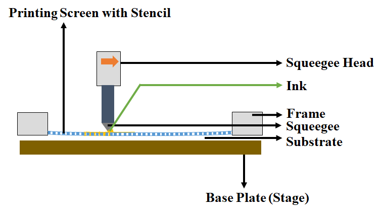
Figure 1. Schematic of the screen printing process.
2.2. Inkjet Printing
Inkjet printing is a non-impact printing method (NIP), and it uses a digital image signal to print the design by propelling ink droplets onto the substrate instead of any physical image carriers [59,90][49][50]. Typically, in inkjet printing, the inks will be in a liquid state with low viscosities and can be directly printed onto the substrate. Inkjet printing is classified into continuous inkjet printing and drop-on-demand (DOD) inkjet printing. In continuous Inkjet printing, a continuous flow of ink droplets is controlled electronically by a voltage source. Some of the ink droplets are subjected to electrostatic charge and are deflected to get a negative print by electrostatic deflectors while the uncharged drops are used to print the desired image onto the substrate. Thermal inkjet printers are very popular in the graphic printing and packaging industries. In a DOD-based inkjet printing, the ink droplets are created only if it is required by the image signal to get the desired print [59,90][49][50]. The droplets are formed either by using thermal or piezoelectric techniques as shown in Figure 2. In thermal inkjet printers, the ink droplets are forced or impelled out of the cartridge nozzle by a vapor bubble formed because of the vaporization of ink liquid. In piezoelectric inkjet printers, the volume of the cartridge nozzle is mechanically deformed based on the image signal and the ink droplets are released from the nozzle. DOD-based inkjet printing is very popular in FHE and has several advantages including as mask-less fabrication, high print resolution, cost efficiency, and scalability from table-top devices to big press units [90,110,111,112][50][53][54][55].
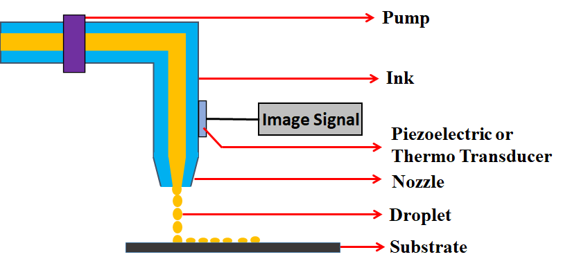
Figure 2. Schematic of the inkjet printing process.
2.3. Gravure Printing
Gravure printing is an impact-based printing technique that provides economical production with fast outputs along with high-quality printing. It uses low viscosity inks and is known for its robustness. The image carrier cylinder (gravure cylinder), doctor blade, ink reservoir, and the impression cylinder are some of the main components of the gravure printer as shown in Figure 3 [59,90][49][50]. Typically, the impression cylinder is made of rubber, the gravure cylinder is made of copper-coated steel, and the doctor blade is manufactured with steel. In gravure printing, the image of the desired design is engraved on the surface of the gravure cylinder. The entire gravure cylinder is flooded by ink from the ink reservoir, and the extra ink is wiped off from the cylinder with the doctor blade prior to printing. The ink is transferred onto the substrate from the gravure cylinder with high pressures, and the substrate movement is controlled by the impression cylinder.
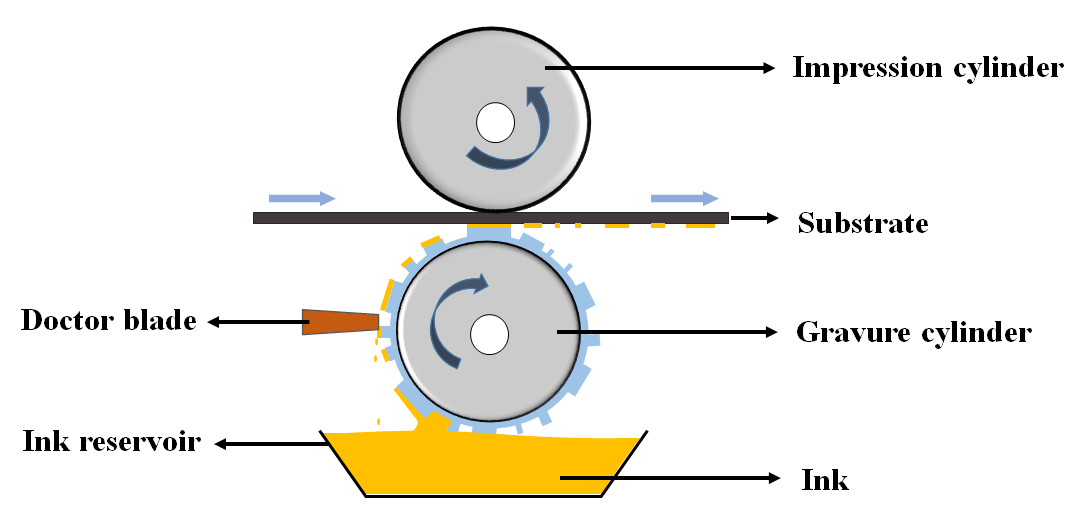
Figure 3. Schematic of the gravure printing process.
2.4. Flexographic Printing
Flexographic printing is a well-established R2R high throughput rotational printing method. It is an indirect impact-based printing technique that can provide a wide range of ink thicknesses with the same resolution. The main parts of the flexographic printer are anilox roller, an impression cylinder, doctor blade, and the ink reservoir (Figure 4) [59,90][49][50]. Anilox roller (a steel cylinder), which has finely engraved cells on its surface made of chromium or ceramics, collects the specific amount of ink from the ink reservoir. Then, the collected ink is transferred onto the elevated structures of the printing plate. With the help of the plate cylinder, the ink on the printing plate is transferred onto the substrate. It is capable of addressing problems such as contact finger geometry as well as production line output. In addition, flexography has high-speed R2R printing capability (up to 100 m per minute) when compared to inkjet and screen printing [138,139][56][57]. Flexography printing is a well-matured printing technique in the graphic printing and packaging industries. However, the implementation of flexographic printing in FHE is not yet explored enough due to the limitations in research and commercial availability of functional inks compatible to flexographic printing. Therefore, there is only limited literature available on the development of flexography-based FHE devices [140,141,142][58][59][60].
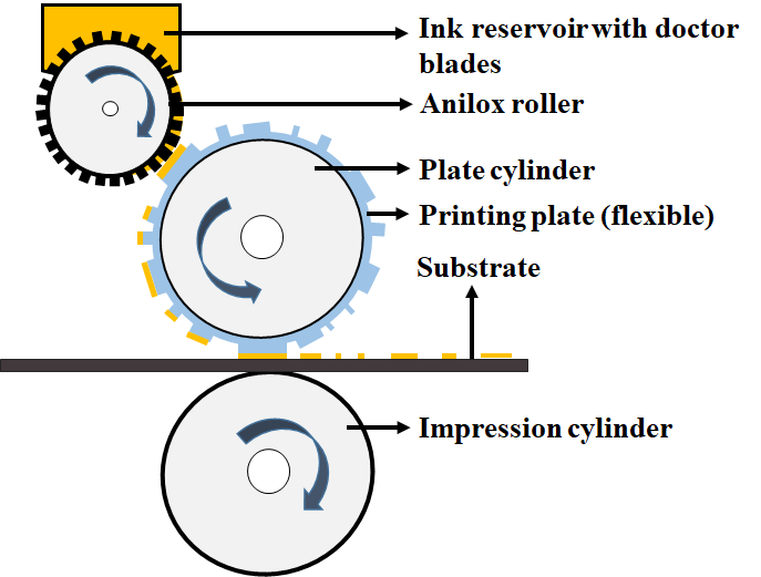
Figure 4. Schematic of the flexography printing process.
References
- Anderson, G.; Anderson, G. The economic impact of technology infrastructure for smart manufacturing, US Department of Commerce. Natl. Inst. Stand. Technol. 2016.
- Ho, C.K.K.; Robinson, A.A.; Miller, D.R.; Davis, M.J. Overview of sensors and needs for environmental monitoring. Sensors 2005, 5, 4–37.
- Lymberis, A. Smart wearables for remote health monitoring, from prevention to rehabilitation: Current R&D, future challenges. In Proceedings of the International IEEE EMBS Special Topic Conference on Information Technology Applications in Biomedicine, Birmingham, UK, 24–26 April 2003; pp. 272–275.
- Wilson, J.S. Sensor Technology Handbook; Elsevier: Amsterdam, The Netherlands, 2004.
- NEXTFLEX Gains $154M in AFRL Funding for 3D Printing Flexible Hybrid Electronics. Available online: https://3dprintingindustry.com/news/nextflex-gains-154m-in-afrl-funding-for-3d-printing-flexible-hybrid-electronics-172700/ (accessed on 12 September 2020).
- Obama Administration Announces New Flexible Hybrid Electronics Manufacturing Innovation Hub in San Jose, CA, USA. Available online: https://obamawhitehouse.archives.gov/the-press-office/2015/08/28/fact-sheet-obama-administration-announces-new-flexible-hybrid (accessed on 12 September 2020).
- FHE Technology & Markets. Available online: https://www.nextflex.us/about/about-fhe/ (accessed on 5 September 2020).
- Khan, Y.; Thielens, A.; Muin, S.; Ting, J.; Baumbauer, C.; Arias, A.C. A New Frontier of Printed Electronics: Flexible Hybrid Electronics. Adv. Mater. 2020, 32, e1905279.
- Maddipatla, D.; Zhang, X.; Bose, A.K.; Masihi, S.; Narakathu, B.B.; Bazuin, B.J.; Williams, J.D.; Mitchell, M.F.; Atashbar, M.Z. A Polyimide Based Force Sensor Fabricated Using Additive Screen-Printing Process for Flexible Electronics. IEEE Access 2020, 8, 207813–207821.
- Perelaer, J.; Smith, P.J.; Mager, D.; Soltman, D.; Volkman, S.K.; Subramanian, V.; Korvink, J.G.; Schubert, U.S. Printed electronics: The challenges involved in printing devices, interconnects, and contacts based on inorganic materials. J. Mater. Chem. 2010, 20, 8446–8453.
- Zhang, X.; Maddipatla, D.; Bose, A.; Hajian, S.; Narakathu, B.B.; Williams, J.D.; Mitchel, M.F.; Atashbar, M.Z. Printed Carbon Nanotubes Based Flexible Resistive Humidity Sensor. IEEE Sens. J. 2020, 20, 12592–12601.
- Maddipatla, D.; Narakathu, B.; Turkani, V.; Bazuin, B.; Atashbar, M. A gravure printed flexible electrochemical sensor for the detection of heavy metal compounds. Multidiscip. Digit. Publ. Inst. Proc. 2018, 2, 950.
- Garlapati, S.K.; Divya, M.; Breitung, B.; Kruk, R.; Hahn, H.; Dasgupta, S. Printed electronics based on inorganic semiconductors: From processes and materials to devices. Adv. Mater. 2018, 30, 1707600.
- Choi, H.W.; Zhou, T.; Singh, M.; Jabbour, G.E. Recent developments and directions in printed nanomaterials. Nanoscale 2015, 7, 3338–3355.
- Chlaihawi, A.A.; Emamian, S.; Narakathu, B.B.; Ali, M.M.; Maddipatla, D.; Bazuin, B.J.; Atashbar, M.Z. A screen printed and flexible piezoelectric-based AC magnetic field sensor. Sens. Actuators A Phys. 2017, 268, 1–8.
- Dyson, M.; Ghaffarzadeh, K. Flexible Hybrid Electronics 2020–2030: Applications, Challenges, Innovations and Forecasts. IDTechEX. 2020. Available online: https://www.idtechex.com/en/research-report/flexible-hybrid-electronics-2020-2030-applications-challenges-innovations-and-forecasts/732 (accessed on 9 October 2020).
- Kim, D.H.; Ahn, J.H.; Choi, W.M.; Kim, H.S.; Kim, T.H.; Song, J.; Huang, Y.Y.; Liu, Z.; Lu, C.; Rogers, J.A. Stretchable and foldable silicon integrated circuits. Science 2008, 320, 507–511.
- Jang, K.I.; Han, S.Y.; Xu, S.; Mathewson, K.E.; Zhang, Y.; Jeong, J.W.; Kim, G.T.; Webb, R.C.; Lee, J.W.; Dawidczyk, T.J.; et al. Rugged and breathable forms of stretchable electronics with adherent composite substrates for transcutaneous monitoring. Nat. Commun. 2014, 5, 1–10.
- Gao, W.; Emaminejad, S.; Nyein, H.Y.Y.; Challa, S.; Chen, K.; Peck, A.; Fahad, H.M.; Ota, H.; Shiraki, H.; Kiriya, D.; et al. Fully integrated wearable sensor arrays for multiplexed in situ perspiration analysis. Nature 2016, 529, 509–514.
- Eshkeiti, A. Novel Stretchable Printed Wearable Sensor for Monitoring Body Movement, Temperature and Electrocardiogram, Along with the Readout Circuit. Ph.D. Thesis, Western Michigan University, Kalamazoo, MI, USA, 2015.
- Yao, S.; Swetha, P.; Zhu, Y. Nanomaterial-Enabled wearable sensors for healthcare. Adv. Healthc. Mater. 2018, 7, 1700889.
- Nakata, S.; Arie, T.; Akita, S.; Takei, K. Wearable, flexible, and multifunctional healthcare device with an ISFET chemical sensor for simultaneous sweat pH and skin temperature monitoring. ACS Sens. 2017, 2, 443–448.
- Martinez, M.M.; Nielsen, J.M.; VanArsdel, K.; Cacace, A.A. Wristband health tracker. U.S. Patent 29/500,837, 21 June 2016.
- Farandos, N.M.; Yetisen, A.K.; Monteiro, M.J.; Lowe, C.R.; Yun, S.H. Contact lens sensors in ocular diagnostics. Adv. Healthc. Mater. 2015, 4, 792–810.
- Abreu, M.M. Contact Lens for Collecting Tears and Detecting Analytes for Determining Health Status, Ovulation Detection, and Diabetes Screening. U.S. Patent 7,809,417, 5 October 2010.
- Kim, S.K.; Koo, J.; Lee, G.H.; Jeon, C.; Mok, J.W.; Mun, B.H.; Lee, K.J.; Kamrani, E.; Joo, C.K.; Shin, S.; et al. Wireless smart contact lens for diabetic diagnosis and therapy. Sci. Adv. 2020, 6, eaba3252.
- Wearables Market Trending Upward. Available online: https://www.printedelectronicsnow.com/issues/2019-11-01/view_features/wearables-market-trending-upward/46378 (accessed on 12 September 2020).
- Cheng, H.; Yi, N. Dissolvable tattoo sensors: From science fiction to a viable technology. Phys. Scr. 2016, 92, 013001.
- Liu, Y.; Wang, H.; Zhao, W.; Zhang, M.; Qin, H.; Xie, Y. Flexible, stretchable sensors for wearable health monitoring: Sensing mechanisms, materials, fabrication strategies and features. Sensors 2018, 18, 645.
- Shetti, N.P.; Mishra, A.; Basu, S.; Mascarenhas, R.J.; Kakarla, R.R.; Aminabhavi, T.M. Skin-Patchable Electrodes for Biosensor Applications: A Review. ACS Biomater. Sci. Eng. 2020, 6, 1823–1835.
- Dinesh, M. Development of Fully Printed and Flexible Strain, Pressure and Electrochemical Sensors. Master’s Thesis, Western Michigan University, Kalamazoo, MI, USA, 2016.
- Suganuma, K. Introduction to Printed Electronics; Springer Science & Business Media: Berlin, Germany, 2014; p. 74. ISBN 978-1-4614-9625-0.
- Liao, Y.; Zhang, R.; Qian, J. Printed electronics based on inorganic conductive nanomaterials and their applications in intelligent food packaging. RSC Adv. 2019, 9, 29154–29172.
- Dahiya, A.S.; Shakthivel, D.; Kumaresan, Y.; Zumeit, A.; Christou, A.; Dahiya, R. High-performance printed electronics based on inorganic semiconducting nano to chip scale structures. Nano Converg. 2020, 7, 1–25.
- Reddy, A.S.G.; Narakathu, B.B.; Eshkeiti, A.; Bazuin, B.J.; Joyce, M.; Atashbar, M.Z. Fully printed organic thin film transistors (OTFT) based flexible humidity sensors. In Proceedings of the IEEE Sensors Conference Proceedings, Baltimore, MD, USA, 3–6 November 2013; pp. 1–4.
- Turkani, V.S.; Maddipatla, D.; Narakathu, B.B.; Bazuin, B.J.; Atashbar, M.Z. A carbon nanotube based NTC thermistor using additive print manufacturing processes. Sens. Actuators A Phys. 2018, 279, 1–9.
- Ali, M.M.; Maddipatla, D.; Narakathu, B.B.; Chlaihawi, A.A.; Emamian, S.; Janabi, F.; Bazuin, B.J.; Atashbar, M.Z. Printed strain sensor based on silver nanowire/silver flake composite on flexible and stretchable TPU substrate. Sens. Actuators A Phys. 2018, 274, 109–115.
- A Wireless Sensing Platform for Every Surface—Boeing’s Condition Monitoring Sensor Array. Available online: http://flex.semi.org/programs-catalog/flex-session-3-fhe-applications/wireless-sensing-platform-every-surface%E2%80%94boeing%E2%80%99s-condition-monitoring-sensor-array (accessed on 12 September 2020).
- Lim, S.; Joyce, M.; Fleming, P.D.; Aijazi, A.T.; Atashbar, M. Inkjet printing and sintering of nano-copper ink. J. Imaging Sci. Technol. 2013, 57, 50506-1–50506-7.
- Tehrani, Z.; Thomas, D.J.; Korochkina, T.; Phillips, C.O.; Lupo, D.; Lehtimaki, S.; Omahony, J.; Gethin, D.T. Large-area printed supercapacitor technology for low-cost domestic green energy storage. Energy 2017, 118, 1313–1321.
- Kang, J.S.; Kim, H.S.; Ryu, J.; Hahn, H.T.; Jang, S.; Joung, J.W. Inkjet printed electronics using copper nanoparticle ink. J. Mater. Sci. Mater. Electron. 2010, 21, 1213–1220.
- Beduk, T.; Bihar, E.; Surya, S.G.; Castillo, A.N.; Inal, S.; Salama, K.N. A paper-based inkjet-printed PEDOT: PSS/ZnO sol-gel hydrazine sensor. Sens. Actuators B Chem. 2020, 306, 127539.
- Arias, A.C.; MacKenzie, J.D.; McCulloch, I.; Rivnay, J.; Salleo, A. Materials and applications for large area electronics: Solution-based approaches. Chem. Rev. 2010, 110, 3–24.
- Wang, X.; Liu, J. Recent advancements in liquid metal flexible printed electronics: Properties, technologies, and applications. Micromachines 2016, 7, 206.
- Chang, W.Y.; Fang, T.H.; Lin, H.J.; Shen, Y.T.; Lin, Y.C. A large area flexible array sensors using screen printing technology. J. Disp. Technol. 2009, 5, 178–183.
- Stringer, J.; Althagathi, T.M.; Tse, C.C.; Ta, V.D.; Shephard, J.D.; Esenturk, E.; Connaughton, C.; Wasley, T.J.; Li, J.; Kay, R.W.; et al. Integration of additive manufacturing and inkjet printed electronics: A potential route to parts with embedded multifunctionality. Manuf. Rev. 2016, 3, 12.
- Katerinopoulou, D.; Zalar, P.; Sweelssen, J.; Kiriakidis, G.; Rentrop, C.; Groen, P.; Gelinck, G.H.; van den Brand, J.; Smits, E.C. Large-area all-printed temperature sensing surfaces using novel composite thermistor materials. Adv. Electron. Mater. 2019, 5, 1800605.
- Fu, S.; Tao, J.; Wu, W.; Sun, J.; Li, F.; Li, J.; Huo, Z.; Xia, Z.; Bao, R.; Pan, C. Fabrication of large-area bimodal sensors by all-inkjet-printing. Adv. Mater. Technol. 2019, 4, 1800703.
- Izdebska-Podsiadły, J.; Thomas, S. (Eds.) Printing on Polymers: Fundamentals and Applications; Elsevier: Amsterdam, The Netherlands, 2015; ISBN 0323375006.
- Kipphan, H. Handbook of Print Media: Technologies and Production Methods; Springer: New York, NY, USA, 2001.
- Wu, W. Inorganic nanomaterials for printed electronics: A review. Nanoscale 2017, 9, 7342–7372.
- Metters, J.P.; Kadara, R.O.; Banks, C.E. New directions in screen printed electroanalytical sensors: An overview of recent developments. Analyst 2011, 136, 1067–1076.
- Eggenhuisen, T.M.; Galagan, Y.; Biezemans, A.F.K.V.; Slaats, T.M.W.L.; Voorthuijzen, W.P.; Kommeren, S.; Shanmugam, S.; Teunissen, J.P.; Hadipour, A.; Verhees, W.J.H.; et al. High efficiency, fully inkjet printed organic solar cells with freedom of design. J. Mater. Chem. A 2015, 3, 7255–7262.
- Corzo, D.; Almasabi, K.; Bihar, E.; Macphee, S.; Rosas-Villalva, D.; Gasparini, N.; Inal, S.; Baran, D. Digital Inkjet Printing of High-Efficiency Large-Area Nonfullerene Organic Solar Cells. Adv. Mater. Technol. 2019, 4, 1900040.
- Focus Label Machinery Launches Digital Inkjet Press. Available online: https://www.labelsandlabeling.com/news/new-products/focus-label-machinery-launches-digital-inkjet-press (accessed on 15 September 2020).
- Shrestha, S.; Yerramilli, R.; Karmakar, N.C. Microwave performance of flexo-printed chipless RFID tags. Flex. Print. Electron. 2019, 4, 045003.
- Gordon, S.E.; Dorfman, J.R.; Kirk, D.; Adams, K. Advances in Conductive Inks across Multiple Applications and Deposition Platforms. DuPont Microcircuit Materials. In Proceedings of the IEEE Photonics Conference, Arlington, VA, USA, 9–13 October 2011; Available online: https://smtnet.com/library/files/upload/Conductive-Inks-Advances.pdf (accessed on 5 September 2020).
- Benson, J.; Fung, C.M.; Lloyd, J.S.; Deganello, D.; Smith, N.A.; Teng, K.S. Direct patterning of gold nanoparticles using flexographic printing for biosensing applications. Nanoscale Res. Lett. 2015, 10, 1–8.
- Fung, C.M.; Lloyd, J.S.; Samavat, S.; Deganello, D.; Teng, K.S. Facile fabrication of electrochemical ZnO nanowire glucose biosensor using roll to roll printing technique. Sens. Actuators B Chem. 2017, 247, 807–813.
- Tian, J.; Arbatan, T.; Li, X.; Shen, W. Liquid marble for gas sensing. Chem. Commun. 2010, 46, 4734–4736.