Your browser does not fully support modern features. Please upgrade for a smoother experience.
Please note this is a comparison between Version 5 by Lindsay Dong and Version 4 by Lindsay Dong.
The promising field of organic electronics has ushered in a new era of biosensing technology, thus offering a promising frontier for applications in both medical diagnostics and environmental monitoring.
- organic electronics
- OECT
- OFET
- OPD
- implants
- biosensors
1. Introduction
Organic electronics have emerged as a promising frontier in the field of biosensing, thereby offering innovative and versatile solutions for medical and environmental applications. With the rapid advancement of organic materials and devices, integrating organic electronics into biosensing platforms has unlocked many possibilities for sensitive, real-time, and label-free biological and chemical analyte detection. This convergence of organic electronics and biosensing can revolutionize medical diagnostics, point-of-care testing, wearable health monitoring, and environmental monitoring, among other critical domains.
Based on carbon-based compounds and polymers, organic electronic devices present distinct advantages that make them well-suited for biosensing applications. These materials offer biocompatibility, thereby enabling direct interactions with biological systems without causing adverse reactions, thus making them ideal for implantable biosensors and in vivo monitoring. Additionally, organic materials exhibit exceptional flexibility, thus enabling the development of conformable and wearable biosensing devices that can seamlessly adapt to the human body or environmental surfaces, thus expanding their utility in personalized healthcare and environmental monitoring. The unique electronic properties of organic materials, such as tunability, conductivity, and semiconducting behavior, contribute to their exceptional sensing capabilities. Organic electronic devices, such as organic field-effect transistors (OFETs), organic electrochemical transistors (OECTs), and organic photodetectors (OPDs), have demonstrated high sensitivity, selectivity, and rapid response times, thereby allowing for the accurate detection of target analytes in complex samples.
2. Organic Bioelectronic Materials
2.1. Conducting Polymers
Conducting polymers (CPs), also known as intrinsically conducting polymers (ICPs) or conjugated polymers, are a class of organic materials that exhibit electrical conductivity while maintaining the desirable mechanical properties of polymers. Unlike traditional semiconductors, CPs are intrinsically conductive without requiring any additional dopants. This unique combination of electrical and mechanical properties makes conducting polymers highly attractive for various applications, including electronics, biosensors, actuators, and energy storage devices. The electrical conductivity of conducting polymers arises from the delocalization of the 𝜋 electrons, which occurs through the presence of alternating single and double bonds along their polymer chains. These 𝜋 electrons can move freely through the conjugated system, thereby allowing the movement of charge carriers (electrons and holes), which consequently results in electrical conductivity. CPs possess a valence band (HOMO—highest occupied molecular orbital) and a conduction band (LUMO—lowest unoccupied molecular orbital) [1]. The energy gap between the HOMO and the LUMO determines the material’s band gap, thereby affecting its electrical properties [2]. In their pure, undoped state, organic polymers may behave as insulators or semiconductors due to the large energy gap between the HOMO and the LUMO [3].In the case of CPs, the energy gap (band gap) between the HOMO and the LUMO is relatively small compared to insulators but larger than for true metals. CPs exhibit distinct electrical and mechanical properties, thereby allowing researchers to tailor their performance for specific applications. The electrical conductivity of conducting polymers can be tuned according to various factors such as oxidation state, doping level, and environmental conditions. CPs can be chemically doped or electrochemically doped to enhance their conductivity. By doping, additional charge carriers are introduced into the material, thus increasing the electrical conductivity. Moreover, the mechanical properties of CPs are influenced by factors such as molecular weight, chemical structure, and processing methods. These polymers can be synthesized into various forms, including films, fibers, and coatings, all while retaining conductivity. The flexibility and ease of processability make conducting polymers suitable for applications where traditional inorganic conductors may be limited due to their rigidity. The unique combination of electrical conductivity and mechanical flexibility enables conducting polymers to be used in electronic devices such as organic transistors, flexible displays, and printed circuits.
One of the pioneering conducting polymers is polyaniline (PANI), which first was discovered for its conductive properties in the late 1970s. Since then, several other conducting polymers, such as polythiophene(PTs), polypyrrole (PPy), and poly(3,4-ethylenedioxythioph ene) (PEDOT), have been developed and extensively studied [4]. PEDOT is the most ubiquitous organic mixed ionic/electronic conductor (OMIEC); it constitutes a class of materials exhibiting simultaneous electronic and ionic conductivity [5]. This unique combination of properties makes OMIECs highly valuable for various applications, including electrochemical devices, energy storage systems, actuators, artificial muscles, and biosensors [6]. OMIECs comprise soft organic materials, such as conducting polymers or small organic molecules, that can conduct electrons and ions, thereby offering advantages over traditional electronic or ionic conductors [7]. Figure 1 shows the chemical structures of commonly used conducting polymers.
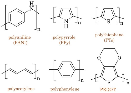
Figure 1. Chemical structures of commonly used conducting polymers: polyaniline (PANI), polypyrrole (PPy), polythiophene(PTs), polyacetylene, polyphenylene, and poly(3,4-ethylenedioxythiophene) (PEDOT).
2.2. Organic Semiconductors
Organic semiconductors are a class of organic materials with unique electronic properties, thus lying between traditional conductors and insulators. The band gap between the organic semiconductors’ valence and conduction bands is relatively lower than in insulators and higher than in conducting polymers. The organic semiconductors are composed of carbon-based molecules or polymers, known as 𝜋-conjugated systems, which enable the movement of charge carriers (electrons and holes) through their conjugated molecular structures [8][9][10][11]. Small-molecule semiconductors consist of discrete, well-defined organic molecules, while polymer-based semiconductors comprise long-chain polymer structures with repeating monomer units. Organic molecules primarily comprise carbon atoms bonded to hydrogen, oxygen, nitrogen, and other elements. Carbon’s ability to form stable covalent bonds with various other atoms allows for the diverse and complex structures found in organic molecules. Organic molecules contain specific functional groups, which are arrangements of atoms that confer distinct chemical properties and reactivity to the molecule. The unique properties of these materials have led to their integration into a wide range of electronic devices, such as organic field-effect transistors (OFETs) [12][13], organic light-emitting diodes (OLEDs) [14][15][16], organic photovoltaics (OPVs) [17][18][19], and organic sensors [20]. OFETs utilize organic semiconductors as the active channel material, thereby enabling flexible and low-power transistor devices. Organic sensors utilize the sensitivity of organic semiconductors to detect changes in environmental parameters, such as gas concentration or biomolecular interactions [21]. Figure 2 shows examples of commonly used small-molecule-based and polymer-based organic semiconductors for different types of bioelectronics devices [22][23][24].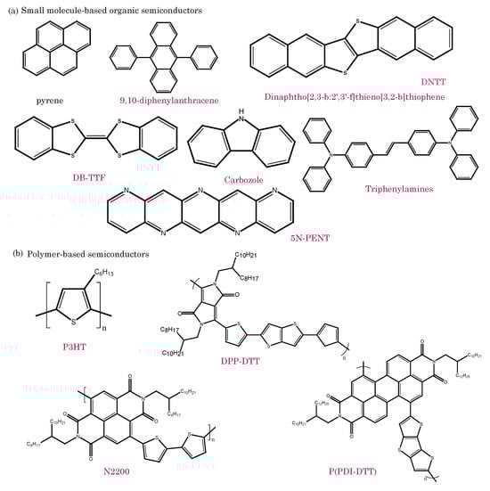
Figure 2. Chemical structures of organic semiconductors: (a) 𝜋-conjugated small molecular families based semiconductors and (b) polymer-based semiconductors.
While organic semiconductors have numerous advantages, such as flexibility and cost-effectiveness, they are not without challenges. These challenges encompass relatively lower charge carrier mobility when compared to their inorganic counterparts, as well as a susceptibility to environmental factors like humidity and temperature, as noted in recent studies [25][26][27]. To overcome these limitations, researchers are actively exploring advanced material engineering, innovative doping techniques, and novel device architectures to enhance the performance and stability of organic semiconductors [28][29].
Organic semiconductors remain a highly promising platform for developing flexible, cost-effective, and energy-efficient electronic devices [30]. Their unique properties and versatile applications have positioned them as compelling candidates for the next generation of electronic and optoelectronic innovations. These advancements drive innovation across various domains, including wearable technology, flexible displays, and renewable energy solutions.
2.3. Biomolecules as Sensing Elements
Biomolecules serve as highly sensitive and selective sensing elements in various biosensing applications. These natural macromolecules, including proteins, nucleic acids, enzymes, and antibodies, exhibit specific interactions with target analytes, thereby enabling the detection and quantification of various substances with remarkable accuracy. The inherent recognition capabilities of biomolecules make them valuable sensing elements in biosensors, thus enabling real-time monitoring of biochemical reactions and detecting of analytes with exceptional specificity.
One of the key advantages of using biomolecules as sensing elements is their ability to bind specifically to target molecules, known as ligands or antigens, through molecular recognition processes [31]. This binding interaction is governed by complementary shapes and chemical properties between the biomolecule’s active sites and the target analyte, thus allowing for highly selective detection [32]. The high affinity of biomolecules to their target analytes ensures that biosensors can distinguish between similar molecules, thus achieving precise and reliable measurements. Various techniques are employed to immobilize biomolecules onto the sensor surface while maintaining biological activity. Surface modification methods, such as physical adsorption, covalent binding, and self-assembled monolayers, allow the biomolecules to remain functional while attached to the sensor surface [33][34][35][36].
Moreover, enzymes are a specific class of biomolecules that are extensively used in biosensing applications due to their catalytic activity [37][38]. Enzymatic biosensors utilize enzymes as sensing elements with a transducer to generate a detectable signal proportional to the concentration of the target analyte. This resulting signal arises from enzymatic reactions that induce changes in proton concentration, gas release/uptake (e.g., ammonia or oxygen), light emission, heat release, and more [39].
Additionally, antibodies are highly specific recognition elements used in immunoassays [40][41]. They can selectively bind to antigens, pathogens, toxins, or specific biomolecules, thereby forming antibody–antigen complexes. These complexes are detectable through various transduction methods, such as optical, electrochemical, or piezoelectric signals, thereby allowing for sensitive and specific detection of the target analyte.
Furthermore, nucleic acids, such as DNA and RNA, are utilized in nucleic acid-based biosensors [42][43][44][45]. These sensing elements recognize specific DNA sequences or RNA targets through hybridization reactions. Nucleic acid biosensors are vital for genetic analysis, disease diagnostics, and the monitoring of nucleic-acid-based biomarkers. Figure 3 illustrates the biomolecule-based biosensors.
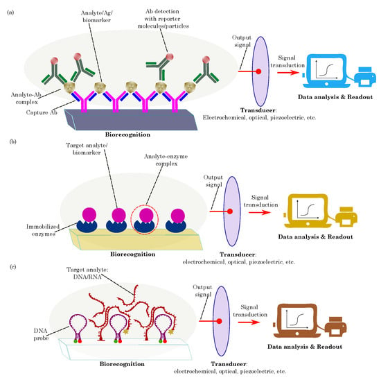
Figure 3. Schematics illustration of biomolecule-based biosensors: (a) antibody-based; (b) enzyme-based biosensors; (c) DNA/RNA-based biosensors.
2.4. Nanomaterials
Nanomaterials are materials that are characterized by nanoscale dimensions, typically ranging from 1 to 100 nm in at least one dimension [46]. These materials exhibit unique properties that differ significantly from their bulk counterparts, thereby making them valuable for various science, engineering, and technology applications. The small size of nanomaterials results in a high surface-to-volume ratio, thus leading to enhanced reactivity and increased surface area for interactions with other materials. This unique feature allows for tailoring their physical, chemical, and mechanical properties through precise size, shape, and composition control [47].
Based on dimensionality, nanomaterials can be categorized into four main categories: zero-dimensional (0D), one-dimensional (1D), two-dimensional (2D), and three-dimensional (3D) nanomaterials (see Figure 4). Zero-dimensional nanomaterials are nanoparticles with nanoscale dimensions in all three directions. Examples include nanoparticles and quantum dots. Nanoparticles comprise metals, metal oxides, semiconductors, polymers, and other materials. Due to their small size, nanoparticles exhibit quantum confinement effects, where their electronic and optical properties become size-dependent. This phenomenon leads to novel optical, electrical, and magnetic behaviors that are different from bulk materials. For example, gold nanoparticles exhibit unique plasmonic properties, thus making them suitable for applications in sensing and imaging [48].
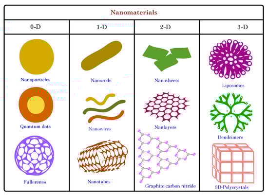
Figure 4. Schematic illustration of nanostructured materials classified based on dimensionality.
One-dimensional (1D) nanomaterials have nanoscale dimensions in two directions, while the third dimension is in the micrometer range. Carbon nanotubes (CNTs) and nanowires are noteworthy examples. CNTs are cylindrical nanostructures of carbon atoms arranged in a hexagonal lattice, thus forming a tubular shape. Due to their unique atomic arrangement, they exhibit remarkable mechanical, electrical, and thermal properties. CNTs can be single-walled (SWCNTs) or multiwalled (MWCNTs), thus exhbiting differing properties based on their structure [49][50].
Two-dimensional (2D) nanomaterials have nanoscale dimensions in one direction while the other two remain relatively larger. The most notable example is graphene, a single layer of carbon atoms arranged in a two-dimensional honeycomb lattice. Graphene has garnered immense attention for its exceptional properties and diverse applications, particularly in biosensing [51][52][53]. Its remarkable electrical conductivity, high surface area, and biocompatibility make it a promising biosensor candidate. Graphene-based biosensors can detect biomolecules with high sensitivity and specificity, as the binding of the target molecules leads to changes in their electrical properties. Its two-dimensional nature enables efficient interaction with biomolecules, thus enhancing sensor performance.
Three-dimensional (3D) nanomaterials are advanced structures that extend into the nanoscale in three spatial dimensions, thus offering unique properties and a high degree of control over their physical and chemical characteristics. These materials are recognized for their exceptional electroactive surface area, which allows for a higher loading capacity of recognition elements, such as antibodies or aptamers, thereby making them highly effective in targeting specific analytes, amplifying signals, and facilitating efficient biosensing with increased sensitivity and specificity. This category includes intricate hierarchical nanoscale structures and nanocomposites, which play a significant role in 3D materials [54]. A notable example of 3D nanomaterials used in biosensing is the utilization of 3D graphene nanostructures.
Other types of classifications of nanomaterials (e.g., organic, carbon, and inorganic) have been extensively discussed in several published articles [55][56]. In biomedicine, nanomaterials have shown significant promise in drug delivery systems, where nanoparticles can be functionalized to carry therapeutic agents and selectively target specific cells or tissues. Additionally, nanomaterials have been utilized in diagnostic imaging and biosensing applications, where their unique properties enable the susceptible and specific detection of biological analytes.
3. Organic Bioelectronic Devices
3.1. Organic Field-Effect Transistors (OFETs)
Organic field-effect transistors (OFETs) are semiconductor devices that utilize organic materials as the active channel to control the flow of charge carriers (electrons or holes) between the source and drain electrodes, and they are modulated by an externally applied electric field at the gate electrode. OFETs have gained considerable attention recently due to their potential for low-cost, flexible, and large-area electronic applications, such as displays, sensors, and integrated circuits [57][58].
The basic structure of an OFET consists of three main components: the source, drain, and gate electrodes, which are all deposited on a substrate. The active channel material, typically an organic semiconductor, forms a thin film between the source and drain electrodes. A gate insulator layer separates the gate electrode from the channel material, and it is often made of an organic or inorganic dielectric [59][60].
One of the significant advantages of OFETs is their compatibility with low-cost, large-area manufacturing processes, such as solution-based deposition techniques like spin coating or inkjet printing. The solution processability of organic semiconductors allows for the fabrication of flexible and stretchable devices on various substrates, including plastic and paper. The versatility of organic materials enables the ability to tailor the active channel’s electronic properties to specific application requirements.
OFETs find applications in various electronic devices, including electronic paper, flexible displays, RFID tags, biosensors, and logic circuits [61]. Additionally, OFET-based sensors have been developed for detecting various environmental and biological analytes, thereby making them attractive for applications in healthcare, environmental monitoring, and point-of-care diagnostics. However, despite their advantages, challenges in OFET technology remain, such as improving their charge carrier mobility, stability, and reproducibility [62][63].
3.2. Organic Electrochemical Transistors (OECTs)
OECTs are electronic devices that utilize organic materials to enable the ion-mediated modulation of electrical conductivity. These transistors have gained significant attention due to their unique properties, such as low operating voltage, biocompatibility, and mechanical flexibility, thereby making them suitable for various applications, including biosensing, neuromorphic computing, and bioelectronics [64]. The basic structure of an OECT consists of three main components: the source, drain, and gate electrodes, which are all integrated into a substrate [65]. The OECT devices work in two modes: depletion and accumulation modes [66]. By default, the depletion mode of the OECT operates with its channel in a conducting (ON) state, thus requiring an applied gate voltage to reduce its conductivity or switch it OFF. This type of organic transistor is constructed using organic semiconductor materials (e.g., PEDOT:PSS) and relies on ion transport within the semiconductor to modulate its conductivity. In contrast, the accumulation mode of the OECT remains in a nonconducting (OFF) state until a negative gate voltage is applied. This voltage accumulates charge carriers within the organic semiconductor channel, thereby allowing the current to flow and turning the transistor ON. Like the depletion mode in OECTs, the accumulation mode in OECTs also employs organic semiconductors (e.g., p(g2T-TT)) and ion transport for its operation, but its default state is nonconductive, thus requiring a gate voltage to activate it. One of the key advantages of OECTs is their biocompatibility, which enables their integration into biological systems without inducing significant adverse effects. This property makes OECTs ideal for interfacing with living cells and tissues, thereby enabling applications in neural interfaces and bioelectronic devices [67]. While OECTs offer numerous advantages, challenges remain in optimizing their stability, reproducibility, and scalability for large-scale production. Researchers continue to explore novel materials, device architectures, and fabrication methods to enhance the performance and reliability of OECTs, thus paving the way for their widespread adoption in cutting-edge electronic and bioelectronic technologies.3.3. Organic Electronic Ion Pumps (OEIPs)
Organic electronic ion pumps represent a burgeoning area of research in bioelectronics, where the principles of organic materials and electronics converge to create advanced systems for ion transport [68][69]. These ion pumps utilize organic materials with specific ion-selective properties to enable the controlled and precise transport of ions, such as cations, anions, protons, or other charged species. The underlying principle involves utilizing organic materials that can change their state, conductivity, or permeability when exposed to external stimuli such as voltage or chemical signals. By applying an electrical potential, these materials can effectively regulate the movement of ions across a membrane or interface. The OEIPs’ capability to manipulate ion transport holds significant implications across diverse domains, ranging from addressing therapeutic challenges through targeted drug delivery and neural modulation to applications in biotechnology and bioengineering. Examples of OEIPs encompass triggering cell signaling in vitro [70][71], controlling epileptiform activity in brain slice models [72], influencing sensory functions in vivo [73], serving as pain therapy in awake animals [74], and even regulating plant growth through the delivery of phytohormones [75]. Organic electronic ion pumps offer several advantages, including biocompatibility, flexibility, and the potential for miniaturization. These properties make them well suited for integration into bioelectronic devices and implantable systems [76][77]. OEIPs can be designed to work in tandem with other components like sensors, actuators, and communication modules. This integration allows for dynamic feedback loops, thus enabling real-time adjustments in ion transport based on physiological responses or external triggers.3.4. Organic Photodetectors (OPDs)
Organic photodetectors (OPDs) are optoelectronic devices that convert incident light into electrical signals through the photoelectric effect, thus utilizing organic materials as the active absorbing layer. These devices have gained significant attention due to their potential for low-cost, flexible, and large-area optoelectronic applications, including image sensors, photodiodes, and light detectors [78]. The basic structure of an organic photodetector typically comprises an organic semiconductor layer sandwiched between two electrodes, which acts as the anode and cathode. The organic semiconductor layer absorbs photons from incident light, thereby generating electron–hole pairs in the material. Depending on the type of OPD, either electrons or holes are transported through the organic layer to the respective electrodes. The operation of an OPD is based on the efficient generation, separation, and collection of photoexcited charge carriers. When photons with energy equal to or greater than the semiconductor band gap are absorbed, excitons (electron–hole pairs) are created. These excitons must be efficiently dissociated into free-charge carriers to generate a photocurrent. To enhance exciton dissociation, OPDs often incorporate donor–acceptor heterojunctions, where the energy levels of the donor and acceptor materials promote efficient charge separation. The photocurrent generated in the organic layer is collected at the electrodes, and the magnitude of the photocurrent is proportional to the intensity of the incident light. Apart from sandwich types, planar-type photodetectors have also been used. These photodetectors are semiconductor devices with a planar structure designed for efficient light detection and conversion into electrical signals. These devices, typically made from semiconductor materials like silicon (Si) and gallium arsenide (GaAs) [79][80][81], operate on a fundamental principle where incident photons with energy greater than the semiconductor’s band gap generate electron–hole pairs when they strike the device’s surface. The resulting free electrons and holes are then separated and collected by an internal electric field, thus creating a photocurrent or a change in voltage, which is directly proportional to the intensity of the incident light. Planar-type photodetectors encompass various designs, including photodiodes, phototransistors, and avalanche photodiodes [82][83][84]. OPDs exhibit high responsivity, a low dark current, and fast response times, thus making them suitable for a wide range of light detection applications. One of the key advantages of OPDs is their compatibility with solution-based deposition techniques, thereby enabling the fabrication of large-area and flexible devices on various substrates. The tunability of organic materials allows for optimizing their light absorption properties to match specific wavelengths or spectral ranges, thus making OPDs versatile for various optical sensing and imaging applications. OPDs are used in diverse optoelectronic devices, such as image sensors [85][86][87], light-sensitive arrays, photodetector arrays [88], and position-sensitive detectors [89][90][91].3.5. Organic Bioelectronic Implants
Organic bioelectronic implants are advanced medical devices integrating organic electronic materials and components into living tissues to enable various therapeutic or diagnostic functionalities. These implants represent a cutting-edge field of research and development in the intersection of organic electronics and biomedicine, thereby offering unique advantages for medical applications [92][93]. Organic bioelectronic implants constitute a complex assembly of crucial components aimed at interfacing with biological systems while delivering therapeutic or monitoring functions. Central to their design are organic semiconductors, conductive polymers like poly(3,4-ethylene dioxythiophene): poly(styrene sulfonate) (PEDOT:PSS), and specialized organic electronic materials meticulously chosen for their biocompatibility, mechanical flexibility, and ability to seamlessly integrate with biological tissues, all while evading significant immune responses [74]. These materials serve as the foundation for the implant’s active elements. Organic bioelectronic implants exhibit adaptability by incorporating sensors to monitor vital physiological parameters like pH, temperature, glucose levels, or specific biomarkers. Additionally, they integrate stimulating components such as electrodes or transducers that are capable of delivering targeted electrical or chemical signals. These signals serve therapeutic objectives such as deep brain stimulation or promoting neural regeneration. To ensure the longevity and efficacy of the implant, it is encapsulated within biocompatible materials or coatings. This encapsulation acts as a protective barrier against unwanted interactions with the surrounding biological environment. Furthermore, these implants harness wireless communication, thereby enabling connectivity with external devices for data collection, remote control, and programming. This breakthrough promises a revolution in patient monitoring and treatment optimization, as demonstrated by recent studies [94][95][96]. They also employ innovative power management systems, including energy harvesting and wireless charging, thus ensuring sustainable operation and reducing the need for frequent battery replacements.4. Fabrication Methods
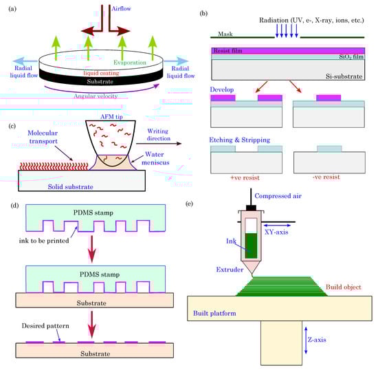
Organic bioelectronic devices are predominantly fabricated/patterned using several approaches, such as organic thin-film deposition methods, patterning techniques, 3D printing, and organic synthesis. Organic thin-film deposition: These methods are widely used for depositing thin films of organic materials on substrates with controlled thickness and uniformity. One common technique is spin coating. In spin coating, an organic material solution, such as semiconductors, conductive polymers, or other active components, is deposited onto a flat substrate, typically a silicon wafer or glass, which can be further integrated into a device (see schematics in Figure 5).Figure 5. Schematic diagram of various fabrication methods: (a) spin-coating process; (b) photolithography; (c) dip-pen nanolithography (DPN); (d) microcontact printing (μCP); (e) direct ink writing (DIW).
Vacuum evaporation is another thin-film deposition method. It facilitates the precise deposition of organic materials onto various substrates under reduced pressure conditions. In this process, organic materials, such as semiconductors, conductive polymers, and other key bioelectronic components, are heated to their vaporization points and then allowed to condense onto the target substrate, thereby creating thin organic films with exceptional uniformity and precise thickness control. This level of control is indispensable in developing organic electronic devices, including organic field-effect transistors (OFETs) and organic photodetectors, where the properties of the organic layer directly influence the device performance. Vacuum evaporation enables the sequential deposition of multiple organic layers, thereby making it possible to design complex device architectures. This capability is invaluable, as organic bioelectronic devices often require distinct functional layers for sensing, signal processing, and data transmission.
Photolithography: It is a well-established technique for patterning organic materials at micron and submicron scales. The photolithography process begins with a substrate, typically made of silicon or glass, that is coated with a layer of photoresist, which is a photosensitive organic material. A photomask containing the desired pattern is placed near the photoresist-coated substrate, and the entire assembly is exposed to ultraviolet (UV) light. The exposed regions undergo a chemical change, thereby making them either more soluble (in the case of positive photoresists) or less soluble (for negative photoresists) in a developer solution, which depends on the type of photoresist used.
Electron-Beam (e-beam) Lithography: Electron-beam lithography or EBL is an advanced nanofabrication technique that operates on the fundamental principle of using a focused beam of electrons to create incredibly fine patterns and structures at the nanometer scale. It has found applications in various fields, including semiconductor device fabrication, nanotechnology, and microelectromechanical systems (MEMS).
Dip-Pen Nanolithography (DPN): DPN is an advanced nanofabrication technique that leverages the precision of scanning probe microscopy (SPM) for the controlled deposition of molecules, nanoparticles, or biomolecules onto a substrate with nanometer-scale precision. In this method, an atomic force microscope (AFM) tip coated with an “ink” material is submerged, or “dipped”, into the ink and then brought into contact with a substrate under the guidance of the AFM.
Microcontact Printing (μCP): μCP is a widely used soft lithography technique employed for precise and controlled deposition of materials, often in the form of self-assembled monolayers (SAMs), on a substrate. The process is akin to conventional rubber stamp printing but on a micro- and nanoscale. μCP employs an elastomeric stamp, usually made of polydimethylsiloxane (PDMS), that is engineered with relief microstructures or patterns on its surface. The stamp is coated with an “ink” or material, which adheres only to the relief patterns. The stamp is then gently brought into contact with a substrate, thereby transferring the material onto the substrate in the desired pattern.
Inkjet Printing: Inkjet printing, a highly versatile technique, has become integral to the realm of organic bioelectronics. The process involves depositing minuscule ink droplets onto a substrate, thus enabling controlled patterning of various functional materials, including organic semiconductors, conductive polymers, and biologically relevant molecules. Its prominence in this field stems from multiple advantages, such as exceptional precision and resolution, broad material compatibility, reduced material wastage due to its additive nature, high levels of customization to adapt complex designs for specific applications, noncontact printing, and scalability that accommodates everything from research-level prototyping to large-scale production [97][98][99][100].
Laser Writing: Laser writing, also known as laser-induced forward transfer (LIFT), is an advanced microfabrication technique that employs a high-intensity laser beam to transfer material from a donor layer to a receiver substrate, thereby enabling the precise deposition of micro- or nanoscale features. A laser pulse generates a shockwave within the donor material, thus propelling a small amount of material toward a transparent receiver substrate placed above it. This method offers exceptional precision, thereby allowing for fine control over the position and size of the deposited material and making it ideal for creating intricate patterns, microarrays, and electronic devices. One of its significant advantages is versatility, as it can be used with various materials, including organic polymers, conductive substances, and biological compounds, thereby making it suitable for applications ranging from organic electronics to biosensors.
3D Printing: The field of bioelectronics has witnessed remarkable progress with the integration of 3D printing technologies. These technologies are known for their streamlined processes, which empower the creation of intricate three-dimensional structures with exceptional precision, scalability, and adaptability [101][102][103]. Various 3D printing techniques, including fuse deposition modeling (FDM), stereolithography (SLA), digital light processing (DLP), selective laser sintering (SLS), and direct ink writing (DIW), have been instrumental in patterning and fabricating materials with diverse strategies.
Chemical Methods: Organic bioelectronic devices can also be fabricated through diverse chemical methods, including polymerization, chemical vapor deposition (CVD), and self-assembly [104][105][106][107][108][109][110]. These methods allow for precise control over the molecular structure of the materials, thereby enabling the design of custom organic semiconductors, conductive polymers, and biocompatible coatings.
5. Biosensing Mechanisms
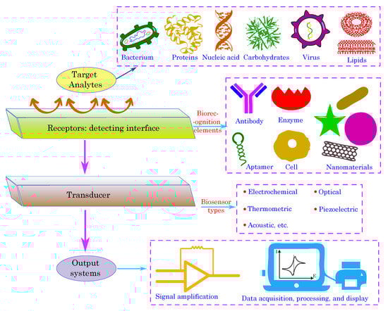
A typical biosensor comprises several fundamental components: the target analytes, receptors or biorecognition elements, a transducer, and output systems [111][112]. The target analyte is the specific substance under investigation, such as glucose, ammonia, alcohol, or lactose. Bioreceptors are biomolecules or biological entities that are capable of recognizing and binding to the target analyte. Examples of biorecognition components include enzymes, cells, aptamers, DNA/RNA strands, and antibodies. The role of the transducer is to convert the biorecognition event into a measurable signal, typically in the form of an electrical signal, which correlates with the quantity or presence of the chemical or biological target. This conversion process is known as signalization. Transducers generate optical or electrical signals that directly correspond to the interactions between the analytes and bioreceptors. Finally, output systems encompass signal processing, amplification, and display units, thereby facilitating the interpretation and presentation of the biosensor’s results. Figure 6 illustrates the components of the typical biosensor.Figure 6. Schematic illustration of key components of a typical biosensor.
5.1. Electrochemical Sensing
Electrochemical sensing is a powerful mechanism that is utilized in organic bioelectronics for detecting and quantifying various biomolecules and chemical species. This sensing platform measures electrical signals generated during electrochemical reactions at the interface between the organic material and the target analyte. Organic electrochemical sensors offer high sensitivity, rapid response times, and excellent selectivity, thereby making them valuable medical diagnostics, environmental monitoring, and point-of-care testing tools. The fundamental principle behind electrochemical sensing in organic bioelectronics lies in the redox properties of organic materials, which can undergo reversible electron transfer reactions [113][114]. These redox-active organic materials, such as conducting polymers, redox enzymes, or organic nanoparticles, are integrated into the sensing platform to act as the transducer element. Electrochemical sensing involves two main components: an electrode and a redox reaction with the target analyte. The sensing platform typically comprises working (or indicator electrode), reference, and counter electrodes (in some cases, the two-electrode system can be used for electrochemical sensing) [115][116]. The working electrode (WE) is coated with the redox-active organic material, where the electrochemical reaction with the target analyte occurs. The reference electrode (RE) maintains a constant potential against which the working electrode’s potential is measured. The counter electrode (CE) completes the electrical circuit and balances the current flow during the electrochemical reaction.
Amperometric Sensing: Amperometric biosensors are a type of electrochemical biosensor used for quantitatively detecting and analyzing biological analytes. These biosensors rely on the measurement of the current generated from an electrochemical redox reaction at the sensor’s working electrode surface when the target analyte interacts with a biorecognition element (such as enzymes, antibodies, or nucleic acids) that is immobilized on the electrode. The basic setup of an amperometric biosensor typically consists of three main components: the working electrode, the reference electrode, and the counter electrode. The biorecognition element is immobilized in the working electrode, and the redox reaction occurs upon the binding of the target analyte. The reference electrode maintains a constant potential, while the counter electrode completes the electrical circuit, thus allowing the flow of electrons during the redox reaction.
Voltammetric Biosensing: Voltammetric biosensors are a type of electrochemical biosensor that rely on the measurement of the current as a function of an applied voltage or potential at the sensor’s working electrode. These biosensors use the principles of voltammetry to detect and quantify the target analyte in a sample. The basic setup of a voltammetric biosensor includes a working electrode coated with a biorecognition element, a reference electrode, and a counter electrode. When an increasing or decreasing voltage is applied to the working electrode, a redox reaction occurs at the electrode surface, involving the oxidation and reduction of electroactive species.
Potentiometric Sensing: Potentiometric biosensors are a type of electrochemical biosensor used for the quantitative detection and analysis of biological analytes. Unlike amperometric biosensors that measure the current generated from a redox reaction, potentiometric biosensors rely on measuring potential or voltage changes at the sensor’s working electrode surface when the target analyte interacts with a biorecognition element. The basic setup of a potentiometric biosensor includes a working electrode and a reference electrode [117]. The working electrode is coated with biorecognition elements, such as enzymes, antibodies, or nucleic acids, which interact with the target analyte in the sample.
Impedimetric Sensing: Impedimetric biosensors are a type of electrochemical biosensor that measure the electrical impedance or resistance changes at the sensor’s working electrode surface in response to the interaction between a biorecognition element and the target analyte.
Impedance-based biosensors can be classified into two main types: capacitive and conductive. Capacitive impedance biosensors rely on changes in the dielectric properties of the interface between the sensing element and the target analyte. When the analyte binds to the immobilized biomolecules, it alters the dielectric constant and thickness of the insulating layer, thereby leading to changes in the electrode’s capacitance. These changes are then measured and related to the concentration of the analyte.
5.2. Optical Sensing
Optical sensing utilizes the interaction between light and organic materials to detect and quantify biological or chemical analytes. These sensing platforms employ organic materials, such as organic semiconductors, fluorescent dyes, or organic nanoparticles, which are integrated into photonic or optoelectronic devices to facilitate the sensitive and selective detection of target molecules. The fundamental principle behind optical sensing in organic bioelectronics relies on the optical properties of the organic materials, which can absorb, emit, or scatter light in response to changes in their environment. Within the realm of optical biosensors, various types have been developed, with each catering to specific applications and detection requirements [118][119].
Surface plasmon resonance (SPR) biosensors, one of the most well-known optical biosensors, rely on the principle of plasmon resonance, which occurs when light interacts with the collective oscillations of electrons on a metal surface [120]. Changes in the refractive index due to binding events on the sensor surface lead to alterations in the resonance angle, thereby enabling the label-free and real-time detection of molecular interactions.
Surface-enhanced Raman scattering (SERS) biosensors leverage the enhancement of Raman scattering signals when molecules are adsorbed on roughened metal surfaces. Molecules adsorbed on these surfaces generate unique Raman spectra, thereby enabling molecular identification and quantification. SERS stands out as an exceptionally sensitive method for identifying low-concentration molecules. It excels in detecting various substances, such as DNA, microRNA, proteins, blood components, and bacteria. Furthermore, it facilitates the detection and characterization of individual cells, aids in bioimaging, and plays a pivotal role in diagnosing various diseases. Its unique ability to offer extensive structural insights into biological analytes adds significant value to the field of analytical science and diagnostics [121].
Fluorescence is a widely used optical phenomenon for biosensing [122]. In fluorescence-based optical sensing, organic fluorescent dyes or fluorophores are used as the sensing elements. When excited with a specific wavelength of light, these fluorescent molecules absorb energy and become excited to higher energy states. Subsequently, they release this excess energy through fluorescence emission at a longer wavelength. The intensity of the emitted fluorescence signal is directly proportional to the concentration of the target analyte, thereby enabling quantitative detection.
Photonic crystal optical biosensors harness the unique properties of photonic crystals to enable the sensitive and specific detection of biomolecular interactions [123]. These biosensors operate on the principle of modifying the transmission or reflection of light when target molecules bind to the sensor surface. Photonic crystals are engineered materials with periodic structures that create band gaps in the electromagnetic spectrum.
Interferometric biosensors utilize the interference patterns generated when light waves interact. By measuring changes in the phase or intensity, these sensors detect biomolecular interactions. Fabry–Perot interferometers and Mach–Zehnder interferometers are commonly used in this category. A Fabry–Perot interferometer exploits multiple-beam interference within a resonant optical cavity to precisely measure the wavelengths of light. It consists of two parallel mirrors with a small separation distance, thus creating a resonant cavity. When light is introduced into the cavity, it reflects repeatedly between these mirrors, thereby leading to constructive and destructive interference between the multiple reflected beams. Constructive interference enhances the intensity of light at specific wavelengths, while destructive interference reduces it at others, thus producing a pattern of interference fringes. By analyzing these fringes and their variations, Fabry–Perot interferometers can be used to determine the wavelengths of light and facilitate high-resolution spectral analysis. Mach–Zehnder interferometers are typically used in integrated optical biosensors.
Optical fiber biosensors employ optical fibers as a core component for detecting and quantifying biological or chemical substances. These sensors are characterized by their capacity to harness light transmission through optical fibers for sensitive and real-time detection. The basic operation typically involves recognition elements, such as antibodies, enzymes, or other bioactive molecules, which are immobilized on the fiber’s surface. When the target analyte binds to this recognition element, it changes the fiber’s optical properties, such as light intensity, wavelength, or polarization. These changes are then quantified and correlated to the concentration of the target analyte. These sensors are compact, versatile, immune to electromagnetic interference, and suitable for remote sensing.
5.3. Piezoelectric Sensing
Piezoelectric biosensing is a powerful and versatile real-time mechanism that is used to detect and quantify biomolecular interactions. This sensing mechanism leverages the piezoelectric effect of certain materials, such as quartz or piezoelectric polymers, to transduce biomolecular binding events into measurable electrical signals. These mass-based biosensors are widely used in biomedical research, diagnostics, and pharmaceutical development due to their label-free, sensitive, and rapid detection capabilities. The fundamental principle behind piezoelectric biosensing lies in the piezoelectric materials’ ability to convert mechanical stress into electrical signals. The biosensing platform typically consists of a piezoelectric transducer, such as a quartz crystal microbalance (QCM) or a piezoelectric polymer-coated cantilever, which is functionalized with specific biorecognition elements [124][125]. These biorecognition elements, such as antibodies, DNA, or enzymes, are carefully immobilized on the surface of the piezoelectric material. When the biosensing platform comes into contact with a biological sample, such as a solution containing biomolecules of interest (e.g., proteins, DNA, or antigens), the biorecognition elements interact selectively with the target biomolecules. This interaction leads to the formation of biomolecular complexes, thereby causing an increase in the mass or stiffness of the layer attached to the piezoelectric material.6. Biosensing Applications
6.1. Medical Diagnostics
Organic bioelectronics have emerged as a promising technology in medical diagnostics, thus offering unique advantages for noninvasive and point-of-care testing. By leveraging organic materials’ electrical and biological properties, organic bioelectronics facilitates the development of sensitive, portable, and cost-effective diagnostic devices [126][127][128]. Organic bioelectronic biosensors have opened up new possibilities in disease biomarker detection, thereby enabling the identification of specific biomolecules in biological fluids like blood, saliva, and urine [129][130]. These biosensors can be customized to detect disease-related biomarkers associated with conditions such as cancer, cardiovascular disorders, and infectious diseases, thereby facilitating early diagnosis and timely intervention. In the realm of diagnostics, organic bioelectronics play a central role in the miniaturization of diagnostic platforms, thus giving rise to lab-on-a-chip (LOC) devices [131][132]. LOC diagnostics offer rapid and multiplexed testing with minimal sample volume requirements, thus making them ideal for point-of-care settings and reducing the strain on centralized healthcare facilities. The use of organic bioelectronics extends to electrochemical and electronic immunoassays, thus providing highly sensitive and specific detection of antigens and antibodies. These assays allow for the precise quantification of disease-related molecules, thus supporting accurate diagnosis and monitoring of disease progression. Nucleic acid analysis is another application of organic bioelectronics, thereby enabling the detection of DNA and RNA sequences associated with genetic disorders and infectious agents [133][134]. This technology is essential for genetic screening, personalized medicine, and pathogen identification. In medical imaging, organic bioelectronics have shown promise in developing imaging probes and contrast agents, thereby enhancing the resolution and sensitivity of imaging techniques like magnetic resonance imaging (MRI) [135][136].6.2. Wearable Health Monitors
Organic bioelectronics have gained considerable traction as a technology for wearable health monitoring systems, thereby offering exceptional versatility and performance. Wearable devices can seamlessly integrate into daily life by leveraging organic materials’ unique properties, including flexibility, biocompatibility, and tunable electronics [137][138]. Applying organic bioelectronic sensors allows for the continuous and noninvasive monitoring of vital signs, such as heart rate [139], blood pressure [140], respiration rate [141][142], body temperature [143], pulse [144], glucose levels in individuals with diabetes [145], pH levels [146], and the human stress hormone cortisol [147]. Also, organic wearable bioelectronics have been widely used for chronic wound biosensing and on-demand therapy administration [148][149]. Furthermore, organic bioelectronics enable the recording of electrocardiogram (ECG) signals for the early detection of cardiac abnormalities while monitoring skin conditions, muscle activity during physical activities, sleep patterns, stress levels, and emotions, thereby contributing to a comprehensive health assessment [150][151][152]. These wearable systems can also track environmental factors like air quality and temperature, as well as provide secure biometric authentication for enhanced data security. By combining diverse functionalities, organic bioelectronics empower individuals to control their health proactively, thus enabling real-time remote monitoring, personalized drug delivery, and improved overall health management and outcomes [153][154]. As research continues, further advancements in organic bioelectronics promise to revolutionize wearable health monitoring technology and its potential impact on healthcare.6.3. Environmental Monitoring
Organic bioelectronics have demonstrated significant promise across diverse environmental monitoring applications due to their unique attributes, cost-effectiveness, and compatibility with biological systems. These applications achieve more efficient and sustainable monitoring solutions by leveraging organic electronic devices. Key areas of organic bioelectronics applications in environmental monitoring include water quality management and monitoring, thereby enabling the real-time detection of various pollutants in water bodies; air quality monitoring to track air pollution levels continuously; and soil health assessment, which all aid in precision agriculture. In water quality management, organic bioelectronics are crucial in detecting and quantifying water pollutants such as heavy metals, organic compounds, and microorganisms [155][156]. Organic bioelectronic sensors offer high sensitivity and selectivity, thereby enabling real-time water quality monitoring in lakes, rivers, and wastewater treatment facilities [157][158]. These sensors can help identify contamination sources, assess the effectiveness of water treatment processes, and ensure compliance with regulatory standards, thereby preserving water resources and safeguarding aquatic ecosystems.6.4. Food Safety and Quality Control
Organic bioelectronics has emerged as a promising technology for food safety and quality control applications [159][160][161][162]. Their unique properties, including biocompatibility and sensitivity to biological molecules, make them well suited for detecting contaminants, spoilage, and quality indicators in food products. Key applications include detecting food contaminants like pesticides and pathogens, monitoring food spoilage, assessing food quality indicators, and detecting allergens. Organic bioelectronics allows for real-time monitoring of food production processes and on-site testing, thus contributing to consistent quality and safety. Additionally, they can be integrated into smart packaging to monitor food quality during storage and transportation. This technology aids in verifying food authenticity, detecting adulteration, and ensuring agricultural production safety by monitoring pesticide residues on crops. Embracing organic bioelectronics in food safety and quality control enhances consumer protection, reduces food waste, and strengthens food safety regulations.87. Conclusions
Organic electronics in biosensing represent a promising and dynamic frontier with far-reaching implications for medical and environmental applications. This exciting convergence of organic materials and bioelectronics has unlocked new opportunities for the precise, sensitive, and real-time detection of biomolecules and chemical species, thereby transforming the landscape of medical diagnostics and environmental monitoring. The unique properties of organic materials, such as biocompatibility, flexibility, and tunability, have paved the way for developing innovative biosensing devices with diverse applications. From implantable biosensors for continuous health monitoring to wearable devices enabling personalized diagnostics, organic bioelectronics offer groundbreaking solutions that bridge the gap between traditional sensing technologies and cutting-edge medical practices. In medical diagnostics, organic bioelectronic sensors offer the potential to revolutionize disease detection and management. These sensors’ label-free and real-time monitoring capabilities enable the rapid and accurate analysis of biomarkers, thereby facilitating early disease diagnosis and tailored treatment plans. Moreover, integrating organic bioelectronics into wearable health monitoring systems empowers individuals to actively participate in their healthcare, thereby promoting proactive and personalized health management. Beyond medical applications, the versatility of organic bioelectronics finds significant relevance in environmental monitoring. From detecting pollutants and toxins to monitoring changes in environmental parameters, organic bioelectronic sensors contribute to sustainable environmental management and conservation efforts. These sensors offer the potential for the rapid and efficient detection of environmental threats, thereby enabling timely interventions and preserving ecological balance. However, as with any emerging technology, organic electronics in biosensing face challenges that warrant attention. Issues related to biocompatibility, stability, scalability, and manufacturing consistency must be addressed to ensure these biosensing platforms’ reliability and long-term performance.References
- Le, T.H.; Kim, Y.; Yoon, H. Electrical and electrochemical properties of conducting polymers. Polymers 2017, 9, 150.
- Brédas, J.L.; Calbert, J.P.; da Silva Filho, D.; Cornil, J. Organic semiconductors: A theoretical characterization of the basic parameters governing charge transport. Proc. Natl. Acad. Sci. USA 2002, 99, 5804–5809.
- Park, S.; Kang, Y.J.; Majd, S. A review of patterned organic bioelectronic materials and their biomedical applications. Adv. Mater. 2015, 27, 7583–7619.
- Ramanavičius, A.; Ramanavičienė, A.; Malinauskas, A. Electrochemical sensors based on conducting polymer—Polypyrrole. Electrochim. Acta 2006, 51, 6025–6037.
- Paulsen, B.D.; Tybrandt, K.; Stavrinidou, E.; Rivnay, J. Organic mixed ionic–electronic conductors. Nat. Mater. 2020, 19, 13–26.
- Lu, Z.; Pavia, A.; Savva, A.; Kergoat, L.; Owens, R.M. Organic microelectrode arrays for bioelectronic applications. Mater. Sci. Eng. R Rep. 2023, 153, 100726.
- Wu, R.; Matta, M.; Paulsen, B.D.; Rivnay, J. Operando characterization of organic mixed ionic/electronic conducting materials. Chem. Rev. 2022, 122, 4493–4551.
- Brütting, W. Physics of Organic Semiconductors; Wiley Online Library: Hoboken, NJ, USA, 2005.
- Köhler, A.; Bässler, H. Electronic Processes in Organic Semiconductors: An Introduction; John Wiley & Sons: Hoboken, NJ, USA, 2015.
- Kunkel, C.; Margraf, J.T.; Chen, K.; Oberhofer, H.; Reuter, K. Active discovery of organic semiconductors. Nat. Commun. 2021, 12, 2422.
- Chen, J.; Zhang, W.; Wang, L.; Yu, G. Recent research progress of organic small-molecule semiconductors with high electron mobilities. Adv. Mater. 2023, 35, 2210772.
- Sun, Y.; Liu, Y.; Zhu, D. Advances in organic field-effect transistors. J. Mater. Chem. 2005, 15, 53–65.
- Zhang, G.; Xie, C.; You, P.; Li, S. Organic field-effect transistors. In Introduction to Organic Electronic Devices; Springer: Berlin/Heidelberg, Germany, 2022; pp. 107–129.
- Dodabalapur, A. Organic light emitting diodes. Solid State Commun. 1997, 102, 259–267.
- Gather, M.C.; Köhnen, A.; Meerholz, K. White organic light-emitting diodes. Adv. Mater. 2011, 23, 233–248.
- Song, J.; Lee, H.; Jeong, E.G.; Choi, K.C.; Yoo, S. Organic light-emitting diodes: Pushing toward the limits and beyond. Adv. Mater. 2020, 32, 1907539.
- Brabec, C.J. Organic photovoltaics: Technology and market. Sol. Energy Mater. Sol. Cells 2004, 83, 273–292.
- Kippelen, B.; Brédas, J.L. Organic photovoltaics. Energy Environ. Sci. 2009, 2, 251–261.
- Inganäs, O. Organic photovoltaics over three decades. Adv. Mater. 2018, 30, 1800388.
- Wu, Y.L.; Fukuda, K.; Yokota, T.; Someya, T. A highly responsive organic image sensor based on a two-terminal organic photodetector with photomultiplication. Adv. Mater. 2019, 31, 1903687.
- Nasri, A.; Petrissans, M.; Fierro, V.; Celzard, A. Gas sensing based on organic composite materials: Review of sensor types, progresses and challenges. Mater. Sci. Semicond. 2021, 128, 105744.
- Hopkins, J.; Fidanovski, K.; Lauto, A.; Mawad, D. All-organic semiconductors for electrochemical biosensors: An overview of recent progress in material design. Front. Bioeng. Biotechnol. 2019, 7, 237.
- Borges-González, J.; Kousseff, C.J.; Nielsen, C.B. Organic semiconductors for biological sensing. J. Mater. Chem. C 2019, 7, 1111–1130.
- Ta, J.; Sun, W.; Lu, L. Organic small molecule semiconductor materials for OFET-based biosensors. Biosens. Bioelectron. 2022, 216, 114667.
- Kim, K.; Yoo, H.; Lee, E.K. New Opportunities for organic semiconducting polymers in biomedical applications. Polymers 2022, 14, 2960.
- Subbarao, N.V.; Gedda, M.; Iyer, P.K.; Goswami, D.K. Organic field-effect transistors as high performance humidity sensors with rapid response, recovery time and remarkable ambient stability. Org. Electron. 2016, 32, 169–178.
- Za’aba, N.K.; Morrison, J.J.; Taylor, D.M. Effect of relative humidity and temperature on the stability of DNTT transistors: A density of states investigation. Org. Electron. 2017, 45, 174–181.
- Kimpel, J.; Michinobu, T. Conjugated polymers for functional applications: Lifetime and performance of polymeric organic semiconductors in organic field-effect transistors. Polym. Int. 2021, 70, 367–373.
- Dong, P.; Yang, L.; Du, G.; Wang, W.; Rolston, N.; Zhang, J. Anion-Modulated Chemical Doping of Organic Hole Conductor Boosts Efficiency and Stability of Perovskite Solar Cells. Adv. Funct. Mater. 2023, 33, 2211304.
- Neupane, G.P.; Ma, W.; Yildirim, T.; Tang, Y.; Zhang, L.; Lu, Y. 2D organic semiconductors, the future of green nanotechnology. Nano Mater. Sci. 2019, 1, 246–259.
- Ranallo, S.; Bracaglia, S.; Sorrentino, D.; Ricci, F. Synthetic Antigen-Conjugated DNA Systems for Antibody Detection and Characterization. ACS Sens. 2023, 8, 2415–2426.
- Kumar, S.; Bhushan, P.; Krishna, V.; Bhattacharya, S. Tapered lateral flow immunoassay based point-of-care diagnostic device for ultrasensitive colorimetric detection of dengue NS1. Biomicrofluidics 2018, 12, 034104.
- Chaki, N.K.; Vijayamohanan, K. Self-assembled monolayers as a tunable platform for biosensor applications. Biosens. Bioelectron. 2002, 17, 1–12.
- Sonawane, M.D.; Nimse, S.B. Surface modification chemistries of materials used in diagnostic platforms with biomolecules. J. Chem. 2016, 2016, 9241378.
- Sandhyarani, N. Surface modification methods for electrochemical biosensors. In Electrochemical Biosensors; Elsevier: Amsterdam, The Netherlands, 2019; pp. 45–75.
- Li, L.; Wang, S.; Xiao, Y.; Wang, Y. Recent advances in immobilization strategies for biomolecules in sensors using organic field-effect transistors. Trans. Tianjin Univ. 2020, 26, 424–440.
- Rocchitta, G.; Spanu, A.; Babudieri, S.; Latte, G.; Madeddu, G.; Galleri, G.; Nuvoli, S.; Bagella, P.; Demartis, M.I.; Fiore, V.; et al. Enzyme biosensors for biomedical applications: Strategies for safeguarding analytical performances in biological fluids. Sensors 2016, 16, 780.
- Gonzalez-Gonzalez, R.B.; Flores-Contreras, E.A.; Gonzalez-Gonzalez, E.; Torres Castillo, N.E.; Parra-Saldivar, R.; Iqbal, H.M. Biosensor constructs for the monitoring of persistent emerging pollutants in environmental matrices. Ind. Eng. Chem. Res. 2022, 62, 4503–4520.
- Mulchandani, A. Principles of enzyme biosensors. In Enzyme and Microbial Biosensors. Methods in Biotechnology; Mulchandani, A., Rogers, K., Eds.; Humana Press: Totowa, NJ, USA, 1998; pp. 3–14.
- Zeng, X.; Shen, Z.; Mernaugh, R. Recombinant antibodies and their use in biosensors. Anal. Bioanal. Chem. 2012, 402, 3027–3038.
- Sharma, S.; Byrne, H.; O’Kennedy, R.J. Antibodies and antibody-derived analytical biosensors. Essays Biochem. 2016, 60, 9–18.
- Hahn, S.; Mergenthaler, S.; Zimmermann, B.; Holzgreve, W. Nucleic acid based biosensors: The desires of the user. Bioelectrochemistry 2005, 67, 151–154.
- Palchetti, I.; Mascini, M. Nucleic acid biosensors for environmental pollution monitoring. Analyst 2008, 133, 846–854.
- Du, Y.; Dong, S. Nucleic acid biosensors: Recent advances and perspectives. Anal. Chem. 2017, 89, 189–215.
- Fu, Z.; Lu, Y.C.; Lai, J.J. Recent advances in biosensors for nucleic acid and exosome detection. Chonnam Med. J. 2019, 55, 86–98.
- Kumar, S.; Bhushan, P.; Bhattacharya, S. Fabrication of nanostructures with bottom-up approach and their utility in diagnostics, therapeutics, and others. In Environmental, Chemical and Medical Sensors—Energy, Environment, and Sustainability; Bhattacharya, S., Agarwal, A., Chanda, N., Pandey, A., Sen, A., Eds.; Springer: Berlin/Heidelberg, Germany, 2018; pp. 167–198.
- Ramya, M.; Kumar, P.S.; Rangasamy, G.; Rajesh, G.; Nirmala, K.; Saravanan, A.; Krishnapandi, A. A recent advancement on the applications of nanomaterials in electrochemical sensors and biosensors. Chemosphere 2022, 308, 136416.
- Jain, P.K.; Huang, X.; El-Sayed, I.H.; El-Sayed, M.A. Review of some interesting surface plasmon resonance-enhanced properties of noble metal nanoparticles and their applications to biosystems. Plasmonics 2007, 2, 107–118.
- Tasis, D.; Tagmatarchis, N.; Bianco, A.; Prato, M. Chemistry of carbon nanotubes. Chem. Rev. 2006, 106, 1105–1136.
- Maruyama, T. Carbon nanotubes. In Handbook of Carbon-Based Nanomaterials; Elsevier: Amsterdam, The Netherlands, 2021; pp. 299–319.
- Pumera, M. Graphene in biosensing. Mater. Today 2011, 14, 308–315.
- Kuila, T.; Bose, S.; Khanra, P.; Mishra, A.K.; Kim, N.H.; Lee, J.H. Recent advances in graphene-based biosensors. Biosens. Bioelectron. 2011, 26, 4637–4648.
- Morales-Narváez, E.; Baptista-Pires, L.; Zamora-Gálvez, A.; Merkoçi, A. Graphene-based biosensors: Going simple. Adv. Mater. 2017, 29, 1604905.
- Byakodi, M.; Shrikrishna, N.S.; Sharma, R.; Bhansali, S.; Mishra, Y.; Kaushik, A.; Gandhi, S. Emerging 0D, 1D, 2D, and 3D nanostructures for efficient point-of-care biosensing. Biosens. Bioelectron. X 2022, 12, 100284.
- Ealia, S.A.M.; Saravanakumar, M.P. A review on the classification, characterisation, synthesis of nanoparticles and their application. IOP Conf. Ser. Mater. Sci. Eng. 2017, 263, 032019.
- Joudeh, N.; Linke, D. Nanoparticle classification, physicochemical properties, characterization, and applications: A comprehensive review for biologists. J. Nanobiotechnol. 2022, 20, 262.
- Berggren, M.; Richter-Dahlfors, A. Organic bioelectronics. Adv. Mater. 2007, 19, 3201–3213.
- Mei, J.; Diao, Y.; Appleton, A.L.; Fang, L.; Bao, Z. Integrated materials design of organic semiconductors for field-effect transistors. J. Am. Chem. Soc. 2013, 135, 6724–6746.
- Horowitz, G. Organic field-effect transistors. Adv. Mater. 1998, 10, 365–377.
- Picca, R.A.; Manoli, K.; Macchia, E.; Sarcina, L.; Di Franco, C.; Cioffi, N.; Blasi, D.; Österbacka, R.; Torricelli, F.; Scamarcio, G.; et al. Ultimately sensitive organic bioelectronic transistor sensors by materials and device structure design. Adv. Funct. Mater. 2020, 30, 1904513.
- Zhang, X.; Pu, Z.; Su, X.; Li, C.; Zheng, H.; Li, D. Flexible organic field-effect transistors-based biosensors: Progress and perspectives. Anal. Bioanal. Chem. 2023, 415, 1607–1625.
- Chan, P.K.L. The Motivation for and Challenges to Scaling Down Organic Field-Effect Transistors. Adv. Electron. Mater. 2019, 5, 1900029.
- Wang, C.; Zhang, X.; Dong, H.; Chen, X.; Hu, W. Challenges and emerging opportunities in high-mobility and low-energy-consumption organic field-effect transistors. Adv. Energy Mater. 2020, 10, 2000955.
- Ajayan, J.; Mohankumar, P.; Mathew, R.; Thoutam, L.R.; Kaushik, B.K.; Nirmal, D. Organic Electrochemical Transistors (OECTs): Advancements and Exciting Prospects for Future Biosensing Applications. IEEE Trans. Electron Devices. 2023, 70, 3401–3412.
- Friedlein, J.T.; McLeod, R.R.; Rivnay, J. Device physics of organic electrochemical transistors. Org. Electron. 2018, 63, 398–414.
- Rivnay, J.; Inal, S.; Salleo, A.; Owens, R.M.; Berggren, M.; Malliaras, G.G. Organic electrochemical transistors. Nat. Rev. Mater. 2018, 3, 17086.
- Chen, S.; Surendran, A.; Wu, X.; Lee, S.Y.; Stephen, M.; Leong, W.L. Recent technological advances in fabrication and application of organic electrochemical transistors. Adv. Mater. Technol. 2020, 5, 2000523.
- Simon, D.T.; Gabrielsson, E.O.; Tybrandt, K.; Berggren, M. Organic bioelectronics: Bridging the signaling gap between biology and technology. Chem. Rev. 2016, 116, 13009–13041.
- Mei, T.; Zhang, H.; Xiao, K. Bioinspired artificial ion pumps. ACS Nano 2022, 16, 13323–13338.
- Isaksson, J.; Kjäll, P.; Nilsson, D.; Robinson, N.; Berggren, M.; Richter-Dahlfors, A. Electronic control of Ca2+ signalling in neuronal cells using an organic electronic ion pump. Nat. Mater. 2007, 6, 673–679.
- Tybrandt, K.; Larsson, K.C.; Kurup, S.; Simon, D.T.; Kjäll, P.; Isaksson, J.; Sandberg, M.; Jager, E.W.; Richter-Dahlfors, A.; Berggren, M. Translating electronic currents to precise acetylcholine–induced neuronal signaling using an organic electrophoretic delivery device. Adv. Mater. 2009, 21, 4442–4446.
- Proctor, C.M.; Slézia, A.; Kaszas, A.; Ghestem, A.; Del Agua, I.; Pappa, A.M.; Bernard, C.; Williamson, A.; Malliaras, G.G. Electrophoretic drug delivery for seizure control. Sci. Adv. 2018, 4, eaau1291.
- Simon, D.T.; Kurup, S.; Larsson, K.C.; Hori, R.; Tybrandt, K.; Goiny, M.; Jager, E.W.; Berggren, M.; Canlon, B.; Richter-Dahlfors, A. Organic electronics for precise delivery of neurotransmitters to modulate mammalian sensory function. Nature Mater. 2009, 8, 742–746.
- Jonsson, A.; Song, Z.; Nilsson, D.; Meyerson, B.A.; Simon, D.T.; Linderoth, B.; Berggren, M. Therapy using implanted organic bioelectronics. Sci. Adv. 2015, 1, e1500039.
- Poxson, D.J.; Karady, M.; Gabrielsson, R.; Alkattan, A.Y.; Gustavsson, A.; Doyle, S.M.; Robert, S.; Ljung, K.; Grebe, M.; Simon, D.T.; et al. Regulating plant physiology with organic electronics. Proc. Natl. Acad. Sci. USA 2017, 114, 4597–4602.
- Jakešová, M.; Sjöström, T.A.; Đerek, V.; Poxson, D.; Berggren, M.; Głowacki, E.D.; Simon, D.T. Wireless organic electronic ion pumps driven by photovoltaics. NPJ Flex. Electron. 2019, 3, 14.
- Strakosas, X.; Seitanidou, M.; Tybrandt, K.; Berggren, M.; Simon, D.T. An electronic proton-trapping ion pump for selective drug delivery. Sci. Adv. 2021, 7, eabd8738.
- Yang, D.; Ma, D. Development of organic semiconductor photodetectors: From mechanism to applications. Adv. Opt. Mater. 2019, 7, 1800522.
- Schmidt, B.; Ross, R. Position-sensitive photodetectors made with standard silicon-planar technology. Sens. Actuators 1983, 4, 439–446.
- Tull, C.; Iwanczyk, J.; Patt, B.; Vilkelis, G.; Eremin, V.; Verbitskaya, E.; Strokan, N.; Il’yashenko, I.; Ivanov, A.; Sidorov, A.; et al. New high sensitivity silicon photodetectors for medical imaging applications. In Proceedings of the 2002 IEEE Nuclear Science Symposium Conference Record, Norfolk, VA, USA, 10–16 November 2002; Volume 1, pp. 4–8.
- Caria, M.; Barberini, L.; Cadeddu, S.; Giannattasio, A.; Rusani, A.; Sesselego, A.; Lai, A.; D’Auria, S.; Dubecky, F. Gallium arsenide photodetectors for imaging in the far ultraviolet region. Appl. Phys. Lett. 2002, 81, 1506–1508.
- Li, J.; Lu, Q.; Dai, H.; Chen, Z.; Fu, Y.; Chen, X. Tricolor narrowband planar perovskite photodetectors based on FP microcavity structure. Opt. Express 2023, 31, 30578–30587.
- Liu, J.J.; Ho, W.J.; Chiang, C.C.; Teng, C.J.; Yu, C.C.; Li, Y.C. Fabrication and Characterization of Planar-Type Top-Illuminated InP-Based Avalanche Photodetector on Conductive Substrate with Operating Speeds Exceeding 10 Gbps. Sensors 2018, 18, 2800.
- Martyniuk, P.; Wang, P.; Rogalski, A.; Gu, Y.; Jiang, R.; Wang, F.; Hu, W. Infrared avalanche photodiodes from bulk to 2D materials. Light. Sci. Appl. 2023, 12, 212.
- Ng, T.N.; Wong, W.S.; Chabinyc, M.L.; Sambandan, S.; Street, R.A. Flexible image sensor array with bulk heterojunction organic photodiode. Appl. Phys. Lett. 2008, 92, 213303.
- Eckstein, R.; Strobel, N.; Rödlmeier, T.; Glaser, K.; Lemmer, U.; Hernandez-Sosa, G. Fully digitally printed image sensor based on organic photodiodes. Adv. Opt. Mater. 2018, 6, 1701108.
- Song, Y.; Zhong, Z.; He, P.; Yu, G.; Xue, Q.; Lan, L.; Huang, F. Doping Compensation Enables High-Detectivity Infrared Organic Photodiodes for Image Sensing. Adv. Mater. 2022, 34, 2201827.
- Calvi, S.; Rapisarda, M.; Valletta, A.; Scagliotti, M.; De Rosa, S.; Tortora, L.; Branchini, P.; Mariucci, L. Highly sensitive organic phototransistor for flexible optical detector arrays. Org. Electron. 2022, 102, 106452.
- Rand, B.P.; Xue, J.; Lange, M.; Forrest, S.R. Thin-film organic position sensitive detectors. IEEE Photonics Technol. Lett. 2003, 15, 1279–1281.
- Cabanillas-Gonzalez, J.; Peña-Rodríguez, O.; Suarez Lopez, I.; Schmidt, M.; Alonso, M.I.; Goni, A.R.; Campoy-Quiles, M. Organic position sensitive photodetectors based on lateral donor-acceptor concentration gradients. Appl. Phys. Lett. 2011, 99, 103305.
- Li, N.; Li, Y.; Cheng, Z.; Liu, Y.; Dai, Y.; Kang, S.; Li, S.; Shan, N.; Wai, S.; Ziaja, A.; et al. Bioadhesive polymer semiconductors and transistors for intimate biointerfaces. Science 2023, 381, 686–693.
- Mariello, M.; Kim, K.; Wu, K.; Lacour, S.P.; Leterrier, Y. Recent advances in encapsulation of flexible bioelectronic implants: Materials, technologies, and characterization methods. Adv. Mater. 2022, 34, 2201129.
- Wu, S.J.; Zhao, X. Tissue adhesive semiconductors. Science 2023, 381, 608–609.
- Ferguson, J.E.; Redish, A.D. Wireless communication with implanted medical devices using the conductive properties of the body. Expert Rev. Med. Devices 2011, 8, 427–433.
- Khan, A.N.; Cha, Y.O.; Giddens, H.; Hao, Y. Recent advances in organ specific wireless bioelectronic devices: Perspective on biotelemetry and power transfer using antenna systems. Engineering 2022, 11, 27–41.
- Tian, X.; Zeng, Q.; Kurt, S.A.; Li, R.R.; Nguyen, D.T.; Xiong, Z.; Li, Z.; Yang, X.; Xiao, X.; Wu, C.; et al. Implant-to-implant wireless networking with metamaterial textiles. Nat. Commun. 2023, 14, 4335.
- Setti, L.; Fraleoni-Morgera, A.; Mencarelli, I.; Filippini, A.; Ballarin, B.; Di Biase, M. An HRP-based amperometric biosensor fabricated by thermal inkjet printing. Sens. Actuators B Chem. 2007, 126, 252–257.
- Weng, B.; Liu, X.; Shepherd, R.; Wallace, G.G. Inkjet printed polypyrrole/collagen scaffold: A combination of spatial control and electrical stimulation of PC12 cells. Synth. Met. 2012, 162, 1375–1380.
- Greco, F.; Zucca, A.; Taccola, S.; Mazzolai, B.; Mattoli, V. Patterned free-standing conductive nanofilms for ultraconformable circuits and smart interfaces. ACS Appl. Mater. Interfaces 2013, 5, 9461–9469.
- Kumar, S.; Bhushan, P.; Pandey, M.; Bhattacharya, S. Additive manufacturing as an emerging technology for fabrication of microelectromechanical systems (MEMS). J. Micromanuf. 2019, 2, 175–197.
- Zhang, Y.; Shi, G.; Qin, J.; Lowe, S.E.; Zhang, S.; Zhao, H.; Zhong, Y.L. Recent progress of direct ink writing of electronic components for advanced wearable devices. ACS Appl. Electron. Mater. 2019, 1, 1718–1734.
- Sreenilayam, S.P.; Ahad, I.U.; Nicolosi, V.; Garzon, V.A.; Brabazon, D. Advanced materials of printed wearables for physiological parameter monitoring. Mater. Today 2020, 32, 147–177.
- Saadi, M.; Maguire, A.; Pottackal, N.T.; Thakur, M.S.H.; Ikram, M.M.; Hart, A.J.; Ajayan, P.M.; Rahman, M.M. Direct ink writing: A 3D printing technology for diverse materials. Adv. Mater. 2022, 34, 2108855.
- Choi, J.W.; Nam, Y.S.; Lee, W.H. Bioelectronic device consisting of self-assembled biomolecules. Curr. Appl. Phys. 2002, 2, 79–84.
- Iost, R.M.; Crespilho, F.N. Layer-by-layer self-assembly and electrochemistry: Applications in biosensing and bioelectronics. Biosens. Bioelectron. 2012, 31, 1–10.
- Wang, M.; Wang, X.; Moni, P.; Liu, A.; Kim, D.H.; Jo, W.J.; Sojoudi, H.; Gleason, K.K. CVD polymers for devices and device fabrication. Adv. Mater. 2017, 29, 1604606.
- Heydari Gharahcheshmeh, M.; Gleason, K.K. Device fabrication based on oxidative chemical vapor deposition (oCVD) synthesis of conducting polymers and related conjugated organic materials. Adv. Mater. Interfaces 2019, 6, 1801564.
- Torricelli, F.; Adrahtas, D.Z.; Bao, Z.; Berggren, M.; Biscarini, F.; Bonfiglio, A.; Bortolotti, C.A.; Frisbie, C.D.; Macchia, E.; Malliaras, G.G.; et al. Electrolyte-gated transistors for enhanced performance bioelectronics. Nat. Rev. Methods Primers 2021, 1, 66.
- Wang, Z.; Bai, H.; Yu, W.; Gao, Z.; Chen, W.; Yang, Z.; Zhu, C.; Huang, Y.; Lv, F.; Wang, S. Flexible bioelectronic device fabricated by conductive polymer–based living material. Sci. Adv. 2022, 8, eabo1458.
- Balakrishnan, G.; Song, J.; Mou, C.; Bettinger, C.J. Recent progress in materials chemistry to advance flexible bioelectronics in medicine. Adv. Mater. 2022, 34, 2106787.
- Macchia, E.; Picca, R.A.; Manoli, K.; Di Franco, C.; Blasi, D.; Sarcina, L.; Ditaranto, N.; Cioffi, N.; Österbacka, R.; Scamarcio, G.; et al. About the amplification factors in organic bioelectronic sensors. Mater. Horiz. 2020, 7, 999–1013.
- Naresh, V.; Lee, N. A review on biosensors and recent development of nanostructured materials-enabled biosensors. Sensors 2021, 21, 1109.
- Grieshaber, D.; MacKenzie, R.; Vörös, J.; Reimhult, E. Electrochemical biosensors-sensor principles and architectures. Sensors 2008, 8, 1400–1458.
- Ronkainen, N.J.; Halsall, H.B.; Heineman, W.R. Electrochemical biosensors. Chem. Soc. Rev. 2010, 39, 1747–1763.
- Cui, L.; Wu, J.; Ju, H. Electrochemical sensing of heavy metal ions with inorganic, organic and bio-materials. Biosens. Bioelectron. 2015, 63, 276–286.
- Shanbhag, M.M.; Manasa, G.; Mascarenhas, R.J.; Mondal, K.; Shetti, N.P. Fundamentals of bio-electrochemical sensing. Chem. Eng. J. Adv. 2023, 16, 100516.
- Wu, J.; Liu, H.; Chen, W.; Ma, B.; Ju, H. Device integration of electrochemical biosensors. Nat. Rev. Bioeng. 2023, 1, 346–360.
- Chen, C.; Wang, J. Optical biosensors: An exhaustive and comprehensive review. Analyst 2020, 145, 1605–1628.
- Singh, A.K.; Mittal, S.; Das, M.; Saharia, A.; Tiwari, M. Optical biosensors: A decade in review. Alex. Eng. J. 2023, 67, 673–691.
- Damborskỳ, P.; Švitel, J.; Katrlík, J. Optical biosensors. Essays Biochem. 2016, 60, 91–100.
- Liang, X.; Li, N.; Zhang, R.; Yin, P.; Zhang, C.; Yang, N.; Liang, K.; Kong, B. Carbon-based SERS biosensor: From substrate design to sensing and bioapplication. NPG Asia Mater. 2021, 13, 8.
- Borisov, S.M.; Wolfbeis, O.S. Optical biosensors. Chem. Rev. 2008, 108, 423–461.
- Khani, S.; Hayati, M. Optical biosensors using plasmonic and photonic crystal band-gap structures for the detection of basal cell cancer. Sci. Rep. 2022, 12, 5246.
- Skládal, P. Piezoelectric biosensors. TrAC Trends Anal. Chem. 2016, 79, 127–133.
- Pohanka, M. Overview of piezoelectric biosensors, immunosensors and DNA sensors and their applications. Materials 2018, 11, 448.
- Koklu, A.; Ohayon, D.; Wustoni, S.; Druet, V.; Saleh, A.; Inal, S. Organic bioelectronic devices for metabolite sensing. Chem. Rev. 2021, 122, 4581–4635.
- Bhalla, N.; Jolly, P.; Formisano, N.; Estrela, P. Introduction to biosensors. In Essays in Biochemistry; Elsevier: Amsterdam, The Netherlands, 2016; Volume 60, pp. 1–8.
- Coles, L.; Oluwasanya, P.W.; Karam, N.; Proctor, C.M. Fluidic enabled bioelectronic implants: Opportunities and challenges. J. Mater. Chem. B 2022, 10, 7122–7131.
- Macchia, E.; Manoli, K.; Di Franco, C.; Picca, R.A.; Österbacka, R.; Palazzo, G.; Torricelli, F.; Scamarcio, G.; Torsi, L. Organic field-effect transistor platform for label-free, single-molecule detection of genomic biomarkers. ACS Sens. 2020, 5, 1822–1830.
- Wang, L.; Xie, H.; Lin, Y.; Wang, M.; Sha, L.; Yu, X.; Yang, J.; Zhao, J.; Li, G. Covalent organic frameworks (COFs)-based biosensors for the assay of disease biomarkers with clinical applications. Biosens. Bioelectron. 2022, 217, 114668.
- Parkula, V.; Berto, M.; Diacci, C.; Patrahau, B.; Di Lauro, M.; Kovtun, A.; Liscio, A.; Sensi, M.; Samorì, P.; Greco, P.; et al. Harnessing selectivity and sensitivity in electronic biosensing: A novel lab-on-chip multigate organic transistor. Anal. Chem. 2020, 92, 9330–9337.
- Macchia, E.; Kovács-Vajna, Z.M.; Loconsole, D.; Sarcina, L.; Redolfi, M.; Chironna, M.; Torricelli, F.; Torsi, L. A handheld intelligent single-molecule binary bioelectronic system for fast and reliable immunometric point-of-care testing. Sci. Adv. 2022, 8, eabo0881.
- Zhang, J.; Lan, T.; Lu, Y. Overcoming major barriers to developing successful sensors for practical applications using functional nucleic acids. Annu. Rev. Anal. Chem. 2022, 15, 151–171.
- Bai, H.; Wang, Y.; Li, X.; Guo, J. Electrochemical nucleic acid sensors: Competent pathways for mobile molecular diagnostics. Biosens. Bioelectron. 2023, 237, 115407.
- Fang, Y.; Li, X.; Fang, Y. Organic bioelectronics for neural interfaces. J. Mater. Chem. C 2015, 3, 6424–6430.
- Lee, G.; Does, M.D.; Avila, R.; Kang, J.; Harkins, K.D.; Wu, Y.; Banks, W.E.; Park, M.; Lu, D.; Yan, X.; et al. Implantable, Bioresorbable Radio Frequency Resonant Circuits for Magnetic Resonance Imaging. Adv. Sci. 2023, 2, 2301232.
- Lin, B.; Wang, M.; Zhao, C.; Wang, S.; Chen, K.; Li, X.; Long, Z.; Zhao, C.; Song, X.; Yan, S.; et al. Flexible organic integrated electronics for self-powered multiplexed ocular monitoring. NPJ Flex. Electron. 2022, 6, 77.
- Kim, S.; Baek, S.; Sluyter, R.; Konstantinov, K.; Kim, J.H.; Kim, S.; Kim, Y.H. Wearable and implantable bioelectronics as eco-friendly and patient-friendly integrated nanoarchitectonics for next-generation smart healthcare technology. EcoMat 2023, 5, e12356.
- Nathan, V.; Jafari, R. Particle filtering and sensor fusion for robust heart rate monitoring using wearable sensors. IEEE J. Biomed. Health Inform. 2017, 22, 1834–1846.
- Kireev, D.; Sel, K.; Ibrahim, B.; Kumar, N.; Akbari, A.; Jafari, R.; Akinwande, D. Continuous cuffless monitoring of arterial blood pressure via graphene bioimpedance tattoos. Nat. Nanotechnol. 2022, 17, 864–870.
- Kano, S.; Kim, K.; Fujii, M. Fast-response and flexible nanocrystal-based humidity sensor for monitoring human respiration and water evaporation on skin. ACS Sens. 2017, 2, 828–833.
- Roy, K.; Ghosh, S.K.; Sultana, A.; Garain, S.; Xie, M.; Bowen, C.R.; Henkel, K.; Schmeiβer, D.; Mandal, D. A self-powered wearable pressure sensor and pyroelectric breathing sensor based on GO interfaced PVDF nanofibers. ACS Appl. Nano Mater. 2019, 2, 2013–2025.
- Trung, T.Q.; Dang, T.M.L.; Ramasundaram, S.; Toi, P.T.; Park, S.Y.; Lee, N.E. A stretchable strain-insensitive temperature sensor based on free-standing elastomeric composite fibers for on-body monitoring of skin temperature. ACS Appl. Mater. Interfaces 2018, 11, 2317–2327.
- Yang, T.H.; Kim, J.U.; Kim, Y.M.; Koo, J.H.; Woo, S.Y. A new blood pulsation simulator platform incorporating cardiovascular physiology for evaluating radial pulse waveform. J. Healthc. Eng. 2019, 2019, 4938063.
- Karpova, E.V.; Shcherbacheva, E.V.; Galushin, A.A.; Vokhmyanina, D.V.; Karyakina, E.E.; Karyakin, A.A. Noninvasive diabetes monitoring through continuous analysis of sweat using flow-through glucose biosensor. Anal. Chem. 2019, 91, 3778–3783.
- Nyein, H.Y.Y.; Gao, W.; Shahpar, Z.; Emaminejad, S.; Challa, S.; Chen, K.; Fahad, H.M.; Tai, L.C.; Ota, H.; Davis, R.W.; et al. A wearable electrochemical platform for noninvasive simultaneous monitoring of Ca2+ and pH. ACS Nano 2016, 10, 7216–7224.
- Parlak, O.; Keene, S.T.; Marais, A.; Curto, V.F.; Salleo, A. Molecularly selective nanoporous membrane-based wearable organic electrochemical device for noninvasive cortisol sensing. Sci. Adv. 2018, 4, eaar2904.
- Wang, C.; Shirzaei Sani, E.; Gao, W. Wearable bioelectronics for chronic wound management. Adv. Funct. Mater. 2022, 32, 2111022.
- Shirzaei Sani, E.; Xu, C.; Wang, C.; Song, Y.; Min, J.; Tu, J.; Solomon, S.A.; Li, J.; Banks, J.L.; Armstrong, D.G.; et al. A stretchable wireless wearable bioelectronic system for multiplexed monitoring and combination treatment of infected chronic wounds. Sci. Adv. 2023, 9, eadf7388.
- Campana, A.; Cramer, T.; Simon, D.T.; Berggren, M.; Biscarini, F. Electrocardiographic recording with conformable organic electrochemical transistor fabricated on resorbable bioscaffold. Adv. Mater. 2014, 26, 3874–3878.
- Ahmed, N.; Zhu, Y. Early detection of atrial fibrillation based on ECG signals. Bioengineering 2020, 7, 16.
- Yang, A.; Song, J.; Liu, H.; Zhao, Z.; Li, L.; Yan, F. Wearable Organic Electrochemical Transistor Array for Skin-Surface Electrocardiogram Mapping Above a Human Heart. Adv. Funct. Mater. 2023, 33, 2215037.
- Kakria, P.; Tripathi, N.; Kitipawang, P. A real-time health monitoring system for remote cardiac patients using smartphone and wearable sensors. Int. J. Telemed. Appl. 2015, 2015, 373474.
- Lee, Y.; Chung, J.W.; Lee, G.H.; Kang, H.; Kim, J.Y.; Bae, C.; Yoo, H.; Jeong, S.; Cho, H.; Kang, S.G.; et al. Standalone real-time health monitoring patch based on a stretchable organic optoelectronic system. Sci. Adv. 2021, 7, eabg9180.
- Tsopela, A.; Laborde, A.; Salvagnac, L.; Ventalon, V.; Bedel-Pereira, E.; Séguy, I.; Temple-Boyer, P.; Juneau, P.; Izquierdo, R.; Launay, J. Development of a lab-on-chip electrochemical biosensor for water quality analysis based on microalgal photosynthesis. Biosens. Bioelectron. 2016, 79, 568–573.
- Cetó, X.; Voelcker, N.H.; Prieto-Simón, B. Bioelectronic tongues: New trends and applications in water and food analysis. Biosens. Bioelectron. 2016, 79, 608–626.
- Jiang, J.; Men, Y.; Pang, T.; Tang, S.; Hou, Z.; Luo, M.; Sun, X.; Wu, J.; Yadav, S.; Xiong, Y.; et al. An integrated supervision framework to safeguard the urban river water quality supported by ICT and models. J. Environ. Manag. 2023, 331, 117245.
- Krkljes, D.; Kitic, G.; Petes, C.; Birgermajer, S.; Stanojev, J.; Bajac, B.; Panic, M.; Radonic, V.; Brceski, I.; Stravs, R.; et al. Multiparameter Water Quality Monitoring System for Continuous Monitoring of Fresh Waters. arXiv 2023, arXiv:2307.11630.
- Scognamiglio, V.; Arduini, F.; Palleschi, G.; Rea, G. Biosensing technology for sustainable food safety. TrAC Trends Anal. Chem. 2014, 62, 1–10.
- Rotariu, L.; Lagarde, F.; Jaffrezic-Renault, N.; Bala, C. Electrochemical biosensors for fast detection of food contaminants–trends and perspective. TrAC Trends Anal. Chem. 2016, 79, 80–87.
- Curulli, A. Electrochemical biosensors in food safety: Challenges and perspectives. Molecules 2021, 26, 2940.
- Du, T.; Huang, L.; Wang, J.; Sun, J.; Zhang, W.; Wang, J. Luminescent metal-organic frameworks (LMOFs): An emerging sensing platform for food quality and safety control. Trends Food Sci. Technol. 2021, 111, 716–730.
More