1. Importance of Thermal Management in GaN-Based Semiconductor Devices
Wide-bandgap semiconductors include various materials, such as GaN, Silicon carbide (SiC), gallium oxide (Ga
2O
3), and diamond
[1]. Among these semiconductors, GaN has gained significant attention in recent years and, particularly, GaN-based high-electron-mobility transistors (HEMTs) have been used widely for RF frequency applications, such as 5G cellular networks, satellite communication, and radar systems
[2].
Initially, AlGaAs/GaAs heterostructures served as the primary channel materials in HEMTs. In recent years, AlGaN/GaN HEMTs have been adopted widely for RF frequency applications. These GaN-based HEMTs have shown significantly higher output powers, thereby surpassing traditional GaAs-based devices by an order of magnitude. Several techniques have been developed to improve the electrical device performance of GaN-based HEMTs, including the mobility, transconductance, cut-off frequency, and output power. However, further improvements have been hindered by significant challenges in thermal management
[3]. The performance and reliability of GaN-based HEMTs are limited by the high channel temperature induced by SHE in the device channel
[4]. Consequently, to prevent significant thermal damage and ensure long-term reliability, the power dissipation of the current GaN-based HEMTs is reduced for operation at 5–6 W/mm in functional systems, although the theoretical power density can exceed 40 W/mm
[5].
The GaN-based HEMTs are conventionally grown on substrates, such as Si, sapphire, and SiC. Si substrates are preferred because of their low-cost mass production. Sapphire substrates are typically employed for GaN-based LEDs. However, the low thermal conductivity of sapphire limits its suitability for high-power applications. SiC substrates are significantly more expensive than Si and sapphire substrates. However, the smaller lattice mismatch (3.8%) and smaller thermal expansion coefficient mismatch (3.2%) between GaN and SiC enable the growth of GaN-based structures with good crystalline quality, making SiC widely used substrates for power electronic applications. The thermal conductivity of the substrate materials is a key factor to consider in the fabrication of GaN-based semiconductors. The thermal conductivity of the substrate material plays a crucial role in limiting the output power densities of GaN-based HEMTs because the joule heat generated by the SHE is primarily dissipated through the substrate. The thermal conductivities of Si, sapphire, and SiC are approximately 130, 30, and 490 W/mK, respectively
[6]. Accordingly, SiC substrates are conventionally used for fabricating high-power AlGaN/GaN HEMTs. Currently, GaN-on-SiC devices are the standard for high-power RF applications
[7]. Nevertheless, SiC substrates remain inadequate for fully harnessing the total potential of GaN. Among all known natural materials, diamond exhibits the highest thermal conductivity, ranging between 800 and 2000 W/mK, depending on the growth conditions. Diamond has attracted significant interest as a substrate material owing to its exceptional ability to efficiently dissipate heat, surpassing that of SiC
[8]. The GaN-on-diamond shows a three-fold increase in the power density and lower junction temperatures compared with that of a GaN-on-SiC device. However, when GaN is integrated with these substrate materials, the presence of a high TBR at the GaN/substrate interface, which could exceed the intrinsic thermal resistance of the substrate materials, could offset the advantages offered by these high-thermal-conductivity substrates. It has been reported that up to 50% of the channel temperature in AlGaN/GaN HEMTs derives from the TBR of GaN/SiC interfaces for high-quality heteroepitaxy
[9]. Therefore, several advanced experimental techniques have been developed to lower the TBR and fully exploit the high thermal conductivity of these substrates.
2. Effects of TBR on Thermal Management in GaN-on-SiC Devices
Gaska et al. first compared the SHE of AlGaN-GaN HFETs grown on sapphire and 6H-SiC substrates. These authors found that heat dissipation strongly affects the device characteristics soon after the application of the source–drain voltage. Thermal resistance is determined primarily by the substrate rather than the AlGaN-GaN active device layer. However, the TBR between the active device layer and substrate was not measured in this study
[10].
Kuzmík et al.
[11] experimentally investigated and compared the TBR of GaN, Si, SiC, and sapphire substrates. Heterostructures of AlGaN/GaN were grown on different substrates using metal–organic chemical vapor deposition (MOCVD) systems. An AlN nucleation layer of unknown thickness was used. The effective TBR at the GaN/Si interface measured by employing Raman spectroscopy was ~70 m
2 K/GW, which is in good agreement with the value measured by the transient interferometric mapping (TIM) method
[12]. The effective TBR at the GaN/SiC interface was ~120 m
2 K/GW. However, estimating the TBR at the GaN/sapphire interface is difficult because of the relatively low thermal conductivity of sapphire substrates. The authors assumed that the thermal expansion coefficients, substrate roughness, and defects related to the growth techniques influenced the TBR values. Moreover, they investigated the role of the TBR values for different substrates by calculating the steady-state temperature profiles in the cross-sections of the devices. Using the measured TBR, the highest surface temperature was obtained for GaN grown on sapphire (810 K), and the lowest value was obtained for the SiC substrate (420 K).
Employing Raman spectroscopy, Sarua et al.
[13] investigated the TBR of GaN devices grown on various substrates. The effective TBRs of both GaN/Si and GaN/SiC interfaces were determined as ~33 m
2 K/GW. For the GaN device on the sapphire substrate, the TBR was estimated at approximately 120 m
2 K/GW. The determined effective TBR is a combined effect of the TBR because of the phonon mismatch and the reduced thermal conductivity of the GaN layer. Furthermore, the effects of the TBR on the temperature increase in ungated AlGaN/GaN field-effect devices were also investigated. The TBRs of the GaN/Si and GaN/SiC interfaces resulted in an increase in the GaN channel temperature by about 30% and 10% for GaN/SiC and GaN/Si devices, respectively, with respect to the case of negligible TBR at the interface. In comparison, despite the high TBR of GaN/sapphire, the influence of TBR on the temperature increase is much smaller at about 2–4%, which is attributed to the low thermal conductivity of the sapphire substrate.
Cho et al.
[14] measured the effective TBRs of GaN on Si and SiC substrates with 38 nm and 36 nm thick AlN transition layers, respectively. The measured effective TBRs of the GaN/Si and GaN/SiC interfaces were ~7.8 and ~5.3 m
2 K/GW, respectively. An approximate solution to the phonon Boltzmann transport equation was used to present a comprehensive model for the effective resistance of the AlN film, indicating that a combination of point defects within the AlN transition layer and near-interfacial defects could be responsible for the effective TBR.
Chen et al.
[15] conducted a systematic study on the impact of SiC substrate surface pretreatment on the crystalline quality of subsequently grown AlN nucleation layers and GaN buffer layers in an HEMT structure. These authors also investigated the effects of the structural properties on the TBR using Raman thermography, including the surface of the SiC substrate, as well as the crystalline quality, morphology, and thickness of the AlN nucleation layer. The TBR measurements were performed at an interface temperature of GaN/SiC of approximately 160 °C. Surface pretreatment using H
2 on the SiC substrate was performed at different temperatures, varying from 1200 to 1280 °C, prior to the growth of GaN/AlN structures. Characterization using X-ray photoelectron spectroscopy (XPS) revealed that the oxygen- and carbon-related contaminants on the SiC substrates were efficiently removed after H
2 treatment at 1320 °C. The effective TBR was observed to first decrease from ~20 to ~14.5 m
2 K/GW as the pretreatment temperature increased from 1200 to 1220 °C and, subsequently, it increased to ~33 m
2 K/GW as the pretreatment temperature reached 1240 °C. The highest TBR value was measured from the sample containing the superior crystalline quality of the AlN nucleation layer in the series, which could be attributed to the degraded surface morphology of the SiC substrates because of the aggressive H
2 etching process above 1240 °C. This finding revealed the significance of the interfacial structures in the AlN/SiC and AlN/GaN regions in the TBR. Furthermore, by reducing the thickness of the high-quality AlN nucleation layer from 105 to 35 nm, the TBR was reduced from ~33 to ~13 m
2 K/GW.
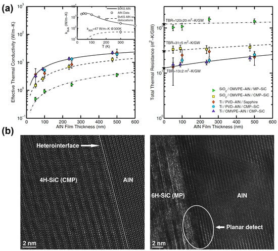
Su et al.
[16] grew AlN thin films on mechanically polished (MP) and chemomechanically polished (CMP) SiC substrates. The TBRs of the AlN/SiC interfaces in the MP and CMP samples were approximately 94 and ~5.1 m
2 K/GW. The intrinsic thermal conductivities of the AlN thin films for both types of samples showed no remarkable differences at ~47 W/mK. The TBR of ~5.1 m
2 K/GW is equivalent to ~240 nm of highly dislocated AlN thin films.
Figure 51a shows the effective thermal conductivity and total thermal resistance as a function of the AlN film thickness on different substrates. These results indicate that the AlN layer made only a small contribution to the overall thermal resistance. Furthermore, the differences in thermal conductivity between films grown on MP and CMP SiC substrates of differing roughness were found to be more significant than the differences owing to the growth method or substrate material. Atomic force microscopy (AFM) characterization showed that the RMS roughness of MP and CMP substrates are ~1.2 and ~0.2 nm, respectively. Compared with that of the CMP substrate, the RMS roughness of the MP substrate, which is six times greater, is considered responsible for its order-of-magnitude-greater TBR. Atomic-resolution TEM imaging revealed that the near-interface planar defects in the AlN films grown on rough SiC were the source of the increased TBR, as shown in
Figure 51b.
Figure 51. (
a) Effective thermal conductivity (
left) and total thermal resistance (
right) as a function of AlN film thickness on different substrates. These plots indicate that the total thermal resistance mainly derives from the TBR rather than the film itself. (
b) Comparison of the atomic-resolution TEM images of the interfaces between AlN/CMP SiC and AlN/MP SiC. AlN grown on CMP 4H-SiC substrate has a clearly defined interface with no apparent additional strain in the film (
left). In contrast, microstructural roughness of the surface of the MP 6H-SiC substrate generates stresses and causes planar defects within the first few atomic layers of the AlN film (
right). (Reprinted from Ref.
[16]. Reproduced with permission from AIP Publishing. All rights reserved).
Feng et al.
[17] reported that a lower TBR of ~20 m
2 K/GW could be achieved by employing an ultrathin AlGaN buffer layer with a low Al content between the GaN films and SiC substrate in comparison with the TBR of ~25 m
2 K/GW for the sample with a 90 nm thick conventional AlN buffer layer. An ultrathin AlGaN buffer layer was introduced through trimethylaluminum pretreatment of the SiC substrates. High-resolution XRD and TEM characterization showed that the dislocation density in the GaN layer could be significantly reduced by using an ultrathin AlN buffer layer. The ultrathin buffer layer not only reduces the TBR at the GaN/SiC interface but also improves the crystal quality of the subsequent GaN layer, which is beneficial for improving the device performance.
AlN nucleation layers are conventionally used to improve the wettability of GaN and SiC. Furthermore, AlN layers are expected to serve as phonon bridges to enhance thermal transport between GaN and SiC. However, using an AlN nucleation layer introduces extrinsic thermal resistance owing to the intrinsic thermal resistance of the AlN layer and the TBRs of the GaN/AlN and AlN/SiC interfaces. Therefore, the TBRs of the GaN/SiC interfaces without an AlN nucleation layer were also investigated. Using an RF-plasma-assisted MBE method, Ziade et al.
[18] deposited an epitaxial GaN layer directly on a SiC substrate without a transition layer. The TBR of the GaN/SiC interface was measured at ~4.3 m
2 K/GW using the FDTR method, which was significantly lower than the TBR for a GaN/SiC interface with an AlN transition layer.
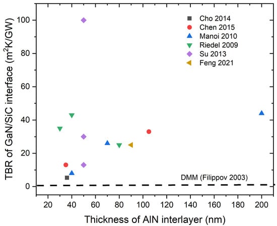
In summary, SiC substrates are conventionally used for GaN-based HEMTs because of their advantages, which include a small mismatch in the lattice and thermal expansion coefficient with GaN and high thermal conductivity. However, the TBR between the GaN device layer and SiC substrate has a significant effect on the thermal management of GaN-on-SiC devices. The TBRs of the GaN/SiC interfaces were measured as exceeding 100 m
2 K/GW in some devices, which is two orders of magnitude higher than the values calculated by the DMM and MD simulations (1–2 m
2 K/GW). The measured TBRs were significantly higher than the intrinsic thermal resistances of the GaN device layer and SiC substrate. An AlN nucleation layer is conventionally used to accommodate the lattice mismatch between the GaN and SiC substrates, resulting in high-quality GaN heteroepitaxy and reduced TBR. However, the TBRs measured by different research groups differed significantly, ranging from 5 to 100 m
2 K/GW, although the same growing methods were used for the AlN nucleation layers. Furthermore, the TBRs of the GaN/AlN/SiC stacks showed no thickness dependence on the AlN nucleation layer. Some samples with an extremely thin AlN nucleation layer showed a high TBR. Most measured TBRs fell within the range of 10–40 m
2 K/GW, as shown in
Figure 62. This finding indicates that the intrinsic thermal resistance of the AlN layer contributes little to the overall thermal resistance of the GaN/AlN/SiC stacks, which is attributed to the high thermal conductivity of the crystalline AlN nucleation layer. These results demonstrate that the growth method and conditions have a significant impact on the microstructure and defect density near the AlN nucleation layer, resulting in a major difference in the measured TBR. In comparison, GaN/SiC interfaces fabricated by the MBE and room-temperature SAB methods with no AlN interlayer have a much lower TBR, which is close to the TBR values predicted by DMM and MD simulations.
Figure 62. TBR of GaN/SiC interface as a function of AlN interlayer thickness
[14][15][16][17][19][20]. TBR predicted by the DMM is also shown for comparison
[21]. Only the data with clear interlayer information are included. The TBRs measured by different research groups differ significantly and show no thickness dependence, ranging from 5 to 100 m
2 K/GW, although the same growth methods are used for growing the AlN nucleation layer.
3. Effects of TBR on Thermal Management in GaN-on-Diamond Devices
Diamond is considered the superior candidate to replace SiC as a substrate for fully exploiting the potential of GaN. Several methods have been employed to integrate GaN with diamond, with the most widely used being the transfer of pregrown GaN from Si to diamond. In this method, the GaN device layer is first grown on a Si substrate, and then polycrystalline diamond is grown by MWCVD on the back of GaN using a transition layer
[22]. The second method involves the direct epitaxial growth of GaN on diamond substrates. However, this method is currently uneconomical owing to the unavailability of large diamond substrates
[23]. The last method involves direct bonding of diamond wafers to GaN, such as SAB. In this method, the surfaces of diamond and GaN are irradiated simultaneously by an Ar fast atom beam and, after completion of the irradiation process, the diamond and GaN are brought into contact by applying a load for a period
[24][25].
Waller et al.
[26] prepared a GaN/diamond interface by directly growing diamonds on GaN (van der Waals bonding). The measured TBR of the GaN/diamond interface was approximately 220 m
2 K/GW, closely matching the value calculated using the weakly bonded AMM model (200 m
2 K/GW). This value is much higher than that of GaN/diamond with an interlayer. These results indicate that a strong bond is crucial for the successful heterogeneous integration of GaN and diamond, despite the interlayer itself having a lower thermal conductivity and additional extrinsic thermal resistance. A suitable interlayer not only protects the GaN surface during growth but also enables carbide bond formation, which greatly increases the interface adhesion energy and, consequently, facilitates phonon transmission.
To reduce the high TBR of the weakly bonded GaN/diamond interface, an interlayer is required to enhance bonding between GaN and diamond. Numerous research groups have investigated the effects of the interlayer type, including Si, SiC, SiN, and AlN.
Field et al.
[27] prepared two GaN-on-diamond samples (namely, one with diamond grown directly on the AlGaN interlayer and the other incorporating a thin crystalline SiC interlayer between AlGaN and diamond). The measured effective TBRs were ~30 and ~107 m
2 K/GW for the sample with a SiC interlayer and without an interlayer, respectively. The reduced TBR was attributed to the improved adhesion between the SiC and diamond compared with diamond directly on AlGaN because of the increased propensity for carbide bond formation between the SiC and diamond. Stronger carbide bonds aid in the transmission of phonons across the interface, improving heat transport.
Siddique et al.
[28] deposited a hot filament (HF) CVD diamond on an AlGaN/GaN HEMT with a 46 nm thick SiN
x interlayer. Extremely smooth surface morphology of SiN
x was obtained, with an RMS roughness of 0.43 nm. Even with some selective degradation of the in situ SiN
x layer, a >20 nm intact SiN
x remained that protected the underlying GaN layers. The effective TBR of the GaN/diamond interface measured by TDTR was ~52.8 m
2 K/GW.
Mandala et al.
[29] deposited a thick (>100 μm) diamond layer on 250 nm thick AlN layers. These authors found that a thick diamond layer could not be grown on the untreated as-grown AlN surfaces. However, the successful growth of a thick diamond layer was achieved on AlN surfaces pretreated with 10% N
2/H
2 plasma for a minimum of 10 min. The effective TBR of the diamond/AlN interface was measured at approximately 16 m
2 K/GW. Characterization employing XPS revealed that pretreatment increased the oxygen content on the AlN surface. After pretreatment, O-terminated seeds led to reduced stress at the AlN/diamond interface, resulting in a low TBR.
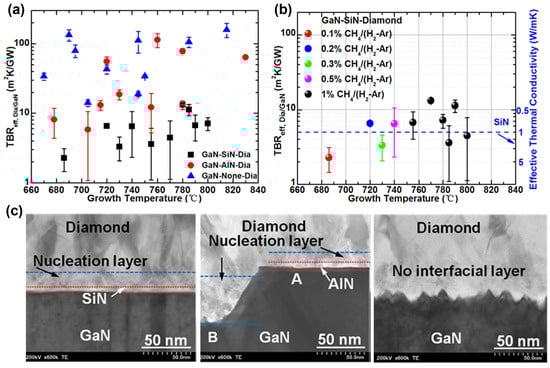
Zhou et al.
[30] fabricated various GaN/diamond interfaces by growing a polycrystalline diamond layer on a GaN device, with SiN and AlN barrier layers, as well as without any barrier layer, using the MPCVD method. These authors measured and systematically compared the effective TBRs of the GaN/diamond interfaces. The results show that an extremely low TBR of ~6.5 m
2 K/GW was obtained by using a 5 nm thick SiN barrier layer, whereas the TBR was ~15.9 and ~61.1 m
2 K/GW for the GaN/diamond interfaces formed by using an AlN barrier layer and without any barrier layer, respectively. In comparison, the DMM-predicted TBR between GaN and diamond was ~3 m
2 K/GW. Furthermore, no clear correlation was observed between the TBR and diamond growth conditions, such as growth temperature and growth recipes, as shown in
Figure 73a,b. The cross-sectional TEM images of the GaN/diamond interfacial region in
Figure 73c shows that the low effective TBR of the GaN/SiN/diamond structures could be attributed to the smooth diamond/SiN and SiN/GaN interfaces, leading to low phonon scattering rates. For the GaN/AlN/diamond structures, both the rougher interface and the thicker diamond nucleation layer are responsible for the higher TBR compared with those grown with the SiN barrier layer. When no barrier layer was used, an even larger roughness was observed at the interface between GaN and diamond, resulting in significantly higher TBR.
Figure 73. (
a) Effective TBRs of GaN/diamond interfaces with different interlayers prepared under various diamond growth temperatures. (
b) Effective TBRs of GaN/SiN/diamond samples as a function of growth temperature for different growth recipes. (
c) Cross-sectional TEM images of GaN-on-diamond interfaces grown with different interlayers of SiN (
left), AlN (
middle), and no interlayer (
right). (Reprinted from Ref.
[30]. Reproduced with permission from ACS Publications. All rights reserved).
Yates et al.
[31] prepared various GaN/diamond interfaces by growing diamonds on three separate structures (namely, a 5 nm thick SiN interfacial layer, a 5 nm thick AlN interfacial layer, and no interfacial layer). The measured effective TBRs of these GaN/diamond interfaces were ~9.5, ~18.2, and ~41.4 m
2 K/GW for the SiN and AlN interfacial layers, and no interlayer, respectively. The results showed a trend in TBR difference similar to that measured by Zhou et al. Cross-sectional TEM imaging demonstrated etching of the GaN device layer by the harsh diamond growth environment when an AlN interfacial layer was used, resulting in a rough interface and increased TBR. When no interlayer was used, the diamond was delaminated completely from the GaN layer for most samples, leading to a significantly high TBR. In comparison, high-resolution TEM imaging and EELS analysis revealed that SiN acts as an etch barrier between the diamond and GaN, and a relatively smooth and ordered elemental transition appears throughout the interlayer, thereby reducing disorder and enhancing phonon transport across the GaN/diamond interface.
Huang et al.
[32] investigated the effects of interlayer materials on the TBR of a diamond/GaN interface using ab initio calculations incorporating the phonon Boltzmann transport equations. The TBRs of three diamond/GaN interfaces with 5 nm thick Si
3N
4, 5 nm thick AlN, and 5 nm thick Si interlayers were calculated at ~4.58, ~5.04, and ~8.48 m
2 K/GW, respectively. This trend in the TBR difference is in good agreement with the experimental results reported by Zhou et al. and Yates et al. In addition, the effect of the interlayer thickness on the TBR was investigated. The results showed that the optimal interlayer thicknesses were approximately 50–60 nm for the AlN interlayer and 70–80 nm for the Si
3N
4 interlayer, matching the spectral phonon transport features. The difference between the experimental and calculated results could be ascribed to the calculations assuming perfectly crystalline interlayer materials without impurities or structural defects. The interlayer materials used in the experiments were either amorphous or contained numerous defects, impurities, and dislocations. In addition, at the nanoscale level, the TBRs measured by different research groups showed substantial measurement uncertainties.
Jia et al.
[33] measured the effective TBRs of two types of GaN/diamond interfaces. One had a 100 nm thick SiN interlayer and the other had a 100 nm thick AlN interlayer. The SiN and AlN interlayers were deposited using radio frequency (RF) magnetron sputtering. The TBRs of samples with the SiN and an AlN interlayers were measured at ~38.5 and ~56.4 m
2 K/GW, respectively, i.e., much higher than the TBRs measured by Zhou et al. and Yates et al. Typically, crystalline SiN and AlN exhibit high thermal conductivities. However, amorphous SiN and AlN thin films deposited by sputtering exhibit much lower thermal conductivities. Therefore, the measured highly effective TBR could be attributed to a thicker interlayer with low thermal conductivity. In addition to the effects of interfacial roughness on the TBR characterized by TEM imaging, the peak shift by XPS analysis demonstrated that compared with AlN, the enhancement in nanodiamond seeding attachment facilitated diamond nucleation and diamond growth on the SiN interlayer, resulting in a lower TBR. Furthermore, interfacial adhesion evaluation using a microscratch test showed that stronger Si–C bonding during diamond nucleation was beneficial for strong film adhesion and lower TBR when SiN was used as an interlayer.
In addition to the effects of the interlayer type, the effects of the SiN interlayer thickness on the TBR have been investigated by several research groups. Sun et al.
[34] measured the effective TBRs of a series of GaN/diamond interfaces with SiN
x interlayers. Two diamond-growth methods were used (namely, HFCVD and MPCVD). Seventeen wafers were prepared, with a SiN
x layer thickness ranging from 28 to 100 nm. These authors found the effective TBR scales with the thickness of the SiN
x interlayers. However, no significant differences were observed among the different diamond growth methods. The effective TBR could be reduced from ~50 to ~12 m
2 K/GW by decreasing the thickness of SiN
x from 100 to 28 nm. From the dependence of TBR on the interlayer thickness, the thermal conductivity of the amorphous SiN
x layer is estimated at ~1.9 W/mK, in agreement with the values for amorphous silicon nitride thin films. Cho et al.
[35] observed reduction by a factor of two in TBR for samples with SiN of different thicknesses. The measured effective TBRs of GaN/diamond interfaces with 22-nm-thick and 31-nm-thick SiN interlayers were ~19.8 and ~31.8 m
2 K/GW, respectively. Furthermore, these authors calculated the GaN/SiN TBR at ~1 m
2 K/GW and the SiN/diamond at ~2 m
2 K/GW using the DMM. Using the calculated DMM value, the intrinsic thermal conductivity of the SiN interlayer was calculated at 1.1–1.5 W/mK. These results show that the low thermal conductivity of the amorphous SiN interlayer is a bottleneck for heat dissipation that needs to be minimized to fully exploit the ultrahigh thermal conductivity of diamond.
Using a combination of Raman thermography and thermal modeling, Pomeroy et al.
[36] investigated the role of the diamond substrate thermal conductivity and GaN/diamond TBR in determining the thermal resistance of GaN-on-diamond devices. Two samples were prepared, one with a 95 μm thick HFCVD diamond layer and a 25 nm thick dielectric interlayer and the other with a 120 μm thick MPCVD diamond layer and a 50 nm thick dielectric interlayer. Based on analyses of the lateral and depth temperature profiles, effective substrate thermal conductivities of ~710 and ~1200 W/mK were obtained for the HFCVD and MPCVD polycrystalline diamond wafers, respectively. Effective TBRs of ~27 and ~36 m
2 K/GW were measured for GaN/diamond interfaces with 25 nm and 50 nm thick proprietary dielectric interlayers, respectively.
Malakoutian et al.
[37] deposited polycrystalline diamond on GaN-based HEMTs using MPCVD. By reducing the thickness of the Si
3N
4 interlayer to ~1 nm, a record low TBR of ~3.1 m
2 K/GW was achieved without damaging the electrical performance of the GaN channel, which is close to the values predicted by DMM. However, if the SiN
x interlayer is too thin, the harsh H
2-plasma diamond growth conditions could etch the GaN device layer underneath and degrade its electrical performance. This challenge requires solving.
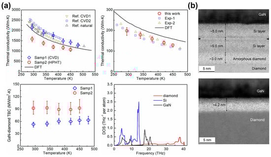
Cheng et al.
[38] bonded GaN and a single-crystal diamond using two modified SAB techniques and measured the effective TBR of the GaN/diamond interfaces. The TBR of the first sample with a sputtering-deposited 10 nm thick Si interlayer (Samp1) was ~19.2 m
2 K/GW. In comparison, a relatively lower TBR of ~10.9 m
2 K/GW was achieved by mixing Si atoms into the Ar ion beam during SAB processing in the second sample (Samp2), which formed a ~4 nm ultrathin interlayer.
Figure 84a shows the temperature dependence of the measured thermal conductivity of the two diamond substrates, the measured thermal conductivity of the GaN layer, the measured TBC of the bonded GaN/diamond interfaces, and the phonon density of states (DOS) of GaN, Si, and diamond. A comparison of the phonon DOS indicates that Si is not an ideal interlayer material from the point of view of phonon DOS mismatch, but it does facilitate strong bonding of GaN with diamond. Therefore, the TBR of bonded GaN/diamond interfaces retains the potential for further reduction using other interfacial layers, such as SiC, AlN, or SiN
x. The cross-sectional TEM images of the two samples in
Figure 84b show that the interlayer thickness in Samp2 was much smaller than that in Samp1, resulting in a relatively lower TBR. Furthermore, device modeling showed that the measured TBR could enable high-power GaN devices by fully exploiting the ultrahigh thermal conductivity of single-crystal diamonds. For the modeled devices, the power density of GaN-on-diamond could reach values ~2.5 times higher than those of GaN-on-SiC and ~5.4 times higher than those of GaN-on-Si with a maximum device temperature of 250 °C.
Figure 84. (
a) Temperature dependence of the measured thermal conductivity of two diamond substrates (
upper left). Measured thermal conductivity of the GaN layer (
upper right). Measured TBC of bonded GaN/diamond interfaces (
lower left), and phonon density of states of GaN, Si, and diamond (
lower right). (
b) Cross-sectional HR-STEM images of GaN/diamond interfaces of Samp1 (
upper) and Samp2 (
lower). (Reprinted from Ref.
[38]. Reproduced with permission from ACS Publications. All rights reserved).
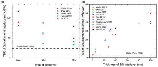
In summary, owing to the substantial mismatch in the phonon DOS, a GaN/diamond interface with no interlayer typically has an extremely high TBR, even higher than 200 m
2 K/GW, which is significantly higher than the intrinsic thermal resistance of GaN active layers and diamond substrates, therefore dictating the total thermal resistance of GaN-on-diamond devices. To reduce the high TBR of GaN/diamond interfaces, interlayers, such as Si, SiC, SiN, and AlN, are typically used to enhance the bonding between GaN and diamond to facilitate phonon transmission, although the interlayer itself, with lower thermal conductivity, introduces additional extrinsic thermal resistance.
Figure 95a shows the effects of the interlayer type on the TBR of the GaN/diamond interfaces. The results demonstrate that using an interlayer decreases the TBR and that SiN as an interlayer is superior to AlN for decreasing TBR. This finding is ascribed to SiN being more difficult to etch than AlN in a harsh diamond growth environment, resulting in a smoother interface and a lower phonon scattering rate at the interface. In addition, the stronger Si–C bonds formed between the diamond and SiN facilitate phonon transport across the interface, resulting in a lower TBR. In addition to the experimental results, the ab initio calculation results showed a similar trend in the TBR difference between different interlayers. Furthermore, the effective TBRs increased along with the increasing thickness of the SiN interlayer, as shown in
Figure 95b. This finding differs from that for the AlN interlayer in GaN-on-SiC devices, where no thickness dependence could be observed. This could be attributed to the thermal conductivity of the crystalline AlN interlayer, which is one order of magnitude higher than that of the amorphous SiN interlayer. Compared with the effects of defects and disorder near the interface, the intrinsic thermal resistance of the AlN interlayer plays a less important role in the total thermal resistance of the GaN/AlN/SiC stacks. Therefore, optimally reducing the thickness of the SiN interlayer is an effective method to reduce the TBR of GaN/SiN/diamond stacks. Although an extremely low TBR of ~3.1 m
2 K/GW has been reported, it remains a challenge to reduce the thickness of a SiN interlayer to ~1 nm to reduce the TBR without affecting the electrical performance of GaN active layers. In addition to decreasing the SiN interlayer thickness, introducing nanostructured interfaces, such as periodically patterned SiN interlayers, could increase the effective contact area and improve the interface bonding strength and seeding density, resulting in a low TBR. The calculation results of the MD simulations also showed similar effects of reducing the TBR using nanostructured interfaces. Furthermore, the room-temperature SAB method is promising for decreasing the TBR.
Figure 95. (
a) Effects of interlayer type on the TBR of GaN/diamond interfaces
[26][30][31][32][33]. Using an interlayer decreases the TBR, with SiN being superior to AlN as interlayer in decreasing TBR. (
b) TBR of GaN/diamond interface as a function of SiN interlayer thickness
[26][30][31][33][34][35][37][39][40][41]. TBR predicted by the DMM is shown for comparison
[30]. Only the data with clear interlayer information are included. The effective TBR increases with the increasing thickness of the SiN interlayer, which differs from the case of an AlN interlayer in GaN-on-SiC devices, where no thickness dependence could be observed.