Your browser does not fully support modern features. Please upgrade for a smoother experience.
Please note this is a comparison between Version 2 by Rita Xu and Version 1 by Carlos Ocampo-López.
Nanoparticle deposition on various substrates has gained significant attention due to the potential applications of nanoparticles in various fields. The deposition techniques covered include electron gun evaporation, physical vapor deposition, plasma enriched chemical vapor deposition (PECVD), electrochemical deposition, chemical vapor deposition, electrophoretic deposition, laser metal deposition, and atomic layer deposition (ALD), thermophoretic deposition, supercritical deposition, spin coating, and dip coating.
- nanomaterials
- nanoparticle deposition
- ceramic substrates
- polymeric substrates
1. Introduction
The rapid development of nanotechnology has revolutionized research in applied sciences, including biomedical, cosmetic, infrastructure, electronics, and food packaging [1]. The production and use of nanomaterials are growing in various industrial processes [2,3,4][2][3][4]. The global market for these materials was valued at 16.3 billion dollars in 2021 [5], and it is projected to reach between 45 billion [6,7][6][7] and 62.8 billion dollars in 2031–2032 [5].
Nanomaterials are generally selected based on their desired applications. They can be synthesized through chemical, physical, or biological methods. Chemical methods involve co-precipitation, chemical reduction of metal salts, electrochemical processes (electrolysis), microemulsion, pyrolysis, photochemical reactions (irradiation), sonochemistry, sol–gel, and solvothermal techniques. Physical methods include arc discharge, electron beam lithography, ion implantation, inert gas condensation, mechanical crushing, grinding, and spray pyrolysis. Biological methods usually rely on biosynthesis approaches using plant extracts, bacteria, fungi, algae, enzymes, and biomolecules [8]. The choice of a specific method often dictates the properties of the particles and the resulting characteristics. Nanomaterials can be synthesized using a bottom-up or top-down approach [9].
Nanomaterials are generally classified based on their production into carbon-based materials, metals, dendrimers, and compounds [10]. Carbon-based nanomaterials typically contain carbon and exist in morphologies such as hollow tubes, ellipsoids, or spheres.
On the other hand, inorganic nanoparticles are produced from carbon-free materials and are classified into two major categories: metals and metal oxide nanoparticles. In most cases, nanoparticles are produced from metals such as platinum (Pt), silver (Ag), gold (Au), cadmium (Cd), cobalt (Co), iron (Fe), copper (Cu), and zinc (Zn) [9,11][9][11].
Metal-based nanomaterials are valuable and have a wide range of applications in various industries, including electronics, medical, dental, textiles, coatings, food packaging, and wastewater treatment [1,6][1][6]. Other emerging potential uses include dispersions and coatings, consolidated materials, biomedicine, and nanodevices [5], and in recent years, the development of nanomaterial applications in consumer products, such as UV filters in sunscreen, odor-resistant textiles, tumor therapies [12], lithium-ion batteries for electric vehicles, and solar panels [13].
Water treatment applications will likely increase the global demand for nanomaterials [6] and the growing demand for electronic products, mainly due to their superparamagnetic properties [14]. With the increasing application of nanomaterials, the industry is also growing, with an estimated direct employment of 300,000 to 400,000 in Europe. These materials are dominant primarily in tire manufacturing as a polymer filler, in toothpaste, or as an anticoagulant in powdered foods [13]. These applications stem from their physicochemical properties and their small size, which result in a high surface area-to-volume ratio, increased reactivity, and ideal optical properties [1], offering a larger surface area compared to the same mass of bulk materials, making them more chemically reactive [15].
Reports by Harish et al. show that nanomaterials exhibit various functionalities such as dimensionality (0–3D), morphology (low and high aspect ratio), porosity (macro-, nano-, mesoporous), composition (carbon, inorganic, organic, and hybrid), origin (natural, incidental, designed, bioinspired), phase (monophasic, multiphasic), and dispersion state (dispersed or aggregated) [16].
Studies by Chaudhary demonstrate that adding nanomaterials modifies the fundamental properties of materials, such as flexibility, durability, flame resistance, barrier properties, and recycling properties [17]. Additionally, material properties can be modified through deposition or doping [18]. This fact can lead to performance improvements, such as the deposition of an anti-reflective coating on the front surface of solar cells, reducing reflection losses by 8% [19], increasing the conductivity of semiconductors [20], improving the barrier properties of bio-based packaging materials [17], enhancing the photocatalytic activity of TiO2 [1], and strengthening materials [21]. Moreover, as nanoparticles are added to a common material, they refine the grain to some extent, forming an intragranular or intergranular structure, thus improving the grain boundary and promoting the mechanical properties of the materials. For example, adding 3% by weight of nano-SiO2 to concrete can improve its compressive strength, flexural strength, and tensile strength by splitting. Adding 3% nano-empty fruit bunch fibers to kenaf epoxy composites can significantly enhance their tensile strength, elongation at break, and impact resistance [22].
Deposition of sacrificial and structural material on the substrate is the first step in surface micromachining and can be achieved through chemical processes such as chemical vapor deposition (CVD), which is commonly used for nanomaterial manufacturing, electrodeposition, vapor phase epitaxy (VPE), and thermal oxidation, or through physical processes such as physical vapor deposition (PVD) and casting [23].
Vapor deposition methods enable a higher-purity surface coating without organometallic compounds. Currently, CVD is the most promising technology for the functionalization of nanoparticles on an industrially relevant scale. This method has multiple variations, including thermally activated, plasma-enhanced, photo-initiated, and oxidative CVD, to name just a few [24].
2. Deposition of Nanoparticles on Ceramic Substrates
The deposition of nanoparticles on different substrates has garnered attention due to the changes it generates in material properties. The functionalization of ceramic substrates has enabled new applications in optical and medical fields, among others. These substrates exhibit different mechanical, optical, electrical, catalytic, and magnetic properties depending on the type of nanoparticle used for functionalization. As a result, new nanoparticle deposition techniques on these substrates have been developed, among which [25,26,27,28,29][25][26][27][28][29] stand out.2.1. Deposition by Electron Gun Evaporation
Electron beam deposition is used to grow thin films of metals with very high melting points or highly pure metals. The precursor is evaporated with gas and then deposited onto the substrate as a film. This method has gained popularity due to its rapid deposition and ability to generate different metal or non-metal film types [30]. In the study conducted by Somayeh Jalilpour et al. [25], tantalum oxide nanolayers were prepared on a glass substrate (1 × 20 × 20) mm3 using an ETS160 system at a pressure of 3 × 10⁻⁷ Torr. The layers were obtained under a high vacuum using the electron gun evaporation method (Edwards E19A3). The purity of tantalum oxide was 99.9%, and the deposition rate was 0.2 Å/s. The substrate temperature was kept constant at 300 K. Before the deposition process, the substrates were cleaned with deionized water, acetone, and ethanol for 15 min each using an ultrasonic method. The thickness of the layers (30, 60, 90, and 120 nm) was measured using a quartz crystal technique (Sigma Instrument, SQM–160, Fort Collins, CO, USA) from the deposition angle of the layers, which was vertically oriented. The study on the coatings’ crystalline nature and morphological evolution was characterized using X-ray diffraction (XRD) and field emission scanning electron microscopy (FESEM), respectively. Surface morphology and roughness were obtained through analysis using an atomic force microscope (AFM) [25].2.2. Physical Vapor Deposition (PVD)
Physical vapor deposition is a vaporization coating technique that involves the transfer of material at the atomic level under vacuum conditions. This technique can be applied to metals, ceramics, and semiconductors. The process is similar to chemical vapor deposition (CVD), except that physical vapor deposition uses a solid precursor instead of a gas-phase precursor in CVD. The process consists of four stages: the evaporation of the material to be deposited or the precursor using a high-energy source such as an electron beam, the transport of vapor to the substrate, the reaction between the substrate atoms and the reactive gas, and finally, the deposition of the coating onto the substrate surface [31] (See Figure 1).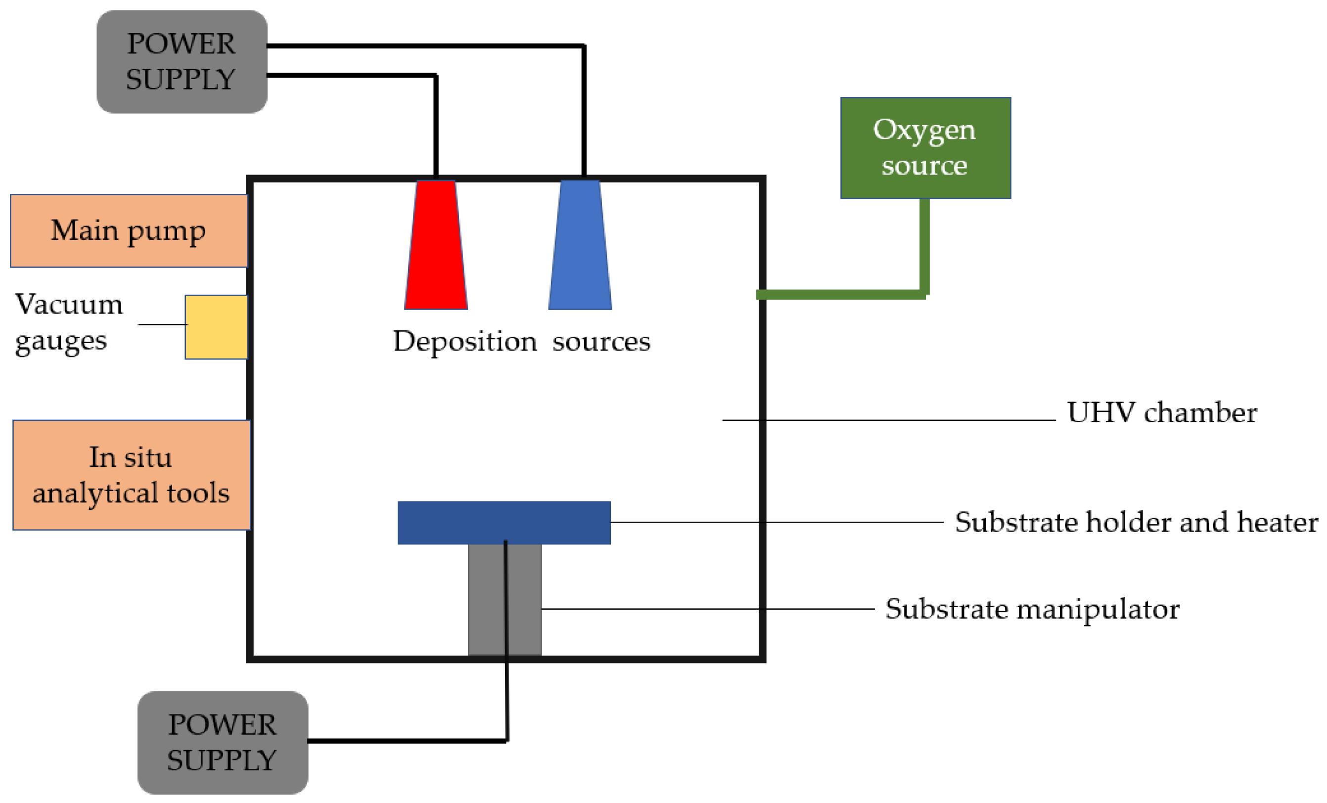
Figure 1. Schematic of a fundamental physical vapor deposition system.
2.3. Plasma-Enhanced Chemical Vapor Deposition (PECVD)
Plasma-enhanced chemical vapor deposition is known as a fast and clean technique for surface modification, where plasma is implemented to achieve more localized and controlled deposition on the substrate. This technique is commonly used on silicon templates to coat them at low temperatures with the desired material and can be applied also to ceramics and polymers. Figure 2 shows a schematic of the plasma-enhanced chemical vapor deposition, where, from the equipment perspective, an inert gas flow is used to prevent secondary reactions, along with a vacuum system and a magnetic field. From the material perspective, the precursor is to be deposited, followed by the target substrate [34][33].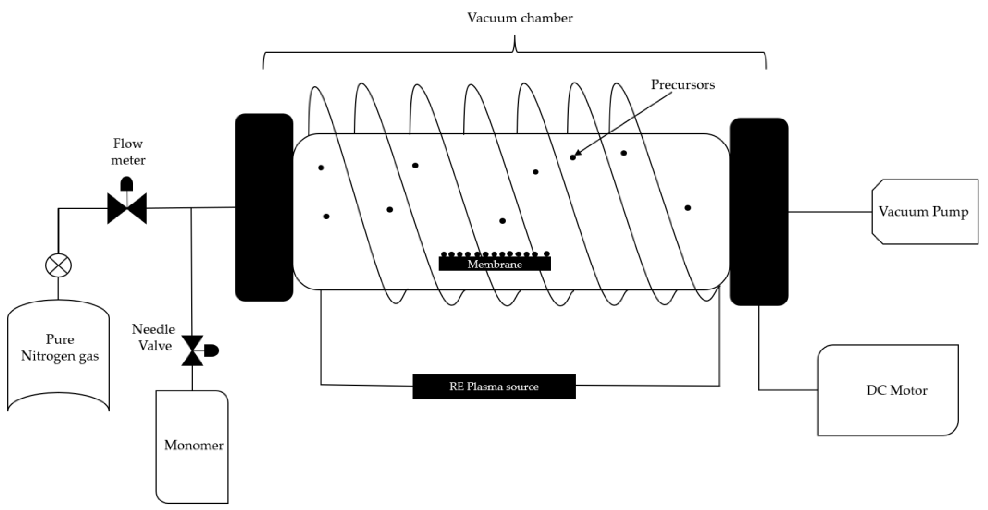
Figure 2. Chemical vapor deposition with enriched plasma.
3. Deposition of Nanomaterials on Polymeric Substrates
The functionalization of polymeric substrates, similar to ceramic substrates, has allowed for new applications of these materials in various areas, including medicine, photonics, and sensors. These substrates exhibit different thermal, mechanical, optical, and catalytic properties depending on the nanomaterial used for functionalization.3.1. Simultaneous and Consecutive Electrochemical Deposition
Nanoparticle electrochemical deposition can be performed through two different pathways, as shown in Figure 3; they are known as simultaneous electrochemical deposition and consecutive electrochemical deposition [46][35]. This technique is applicable also to metal and to ceramic matrices.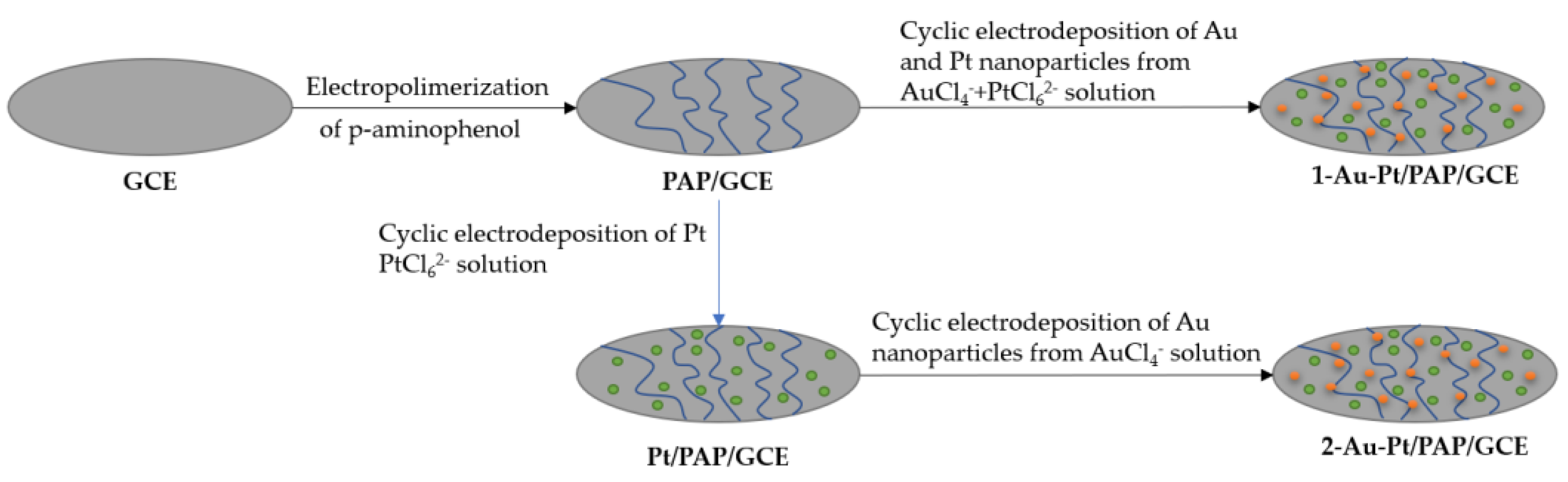
Figure 3. Procedure to design the Au Pt/PAP/GCE.
3.1.1. Simultaneous
In this method, nanoparticles of two different types are simultaneously deposited, as the name implies. As reported by Zekerya Dursun et al. [46][35], electrodes are doped with gold and silver nanoparticles by immersing two electrodes in a solution of chloroauric acid, which serves as the precursor for gold nanoparticles, and potassium hexachloroplatinate, which serves as the precursor for silver nanoparticles. A potential of 0.8 V to −1.1 V is then applied for ten cycles to produce the doping.3.1.2. Consecutive
In this technique, unlike simultaneous deposition, the process is performed in stages, doping first with one material and then with the other. Taking the case of the study by Zekerya Dursun et al. [46][35], for this method, immersion in a solution of potassium hexachloroplatinate is performed with a potential of 0.8 V to −1.1 V, followed by immersion in a solution of chloroauric acid with a potential of 0.1 V to −0.9 V, each for ten cycles.3.2. Chemical Vapor Deposition (CVD)
Chemical vapor deposition follows the same principle as Enriched Chemical Vapor Deposition, the difference being that PECVD introduces precursors with a plasma gas capable of ionizing the precursors. In contrast, CVD introduces chemical precursors into the reaction chamber that thermally decompose to form solid films without plasma [34][33]. The experimental system reported in the study by Hui Kun et al. [39][36] for this technique consists of six parts, as shown in Figure 4: a gas device, a high-temperature furnace, a graphite reaction chamber, a carbon layer sample, a vacuum pump, and a tail gas treatment device. The gas system is divided into two parts, one for argon and the other for propylene, each equipped with a flow meter. The graphite reaction chamber comprises a front graphite channel, a front reaction chamber, a rear reaction chamber, and a rear graphite channel. This design ensures that the reaction gas passes through the porous structure of the carbon layer sample completely.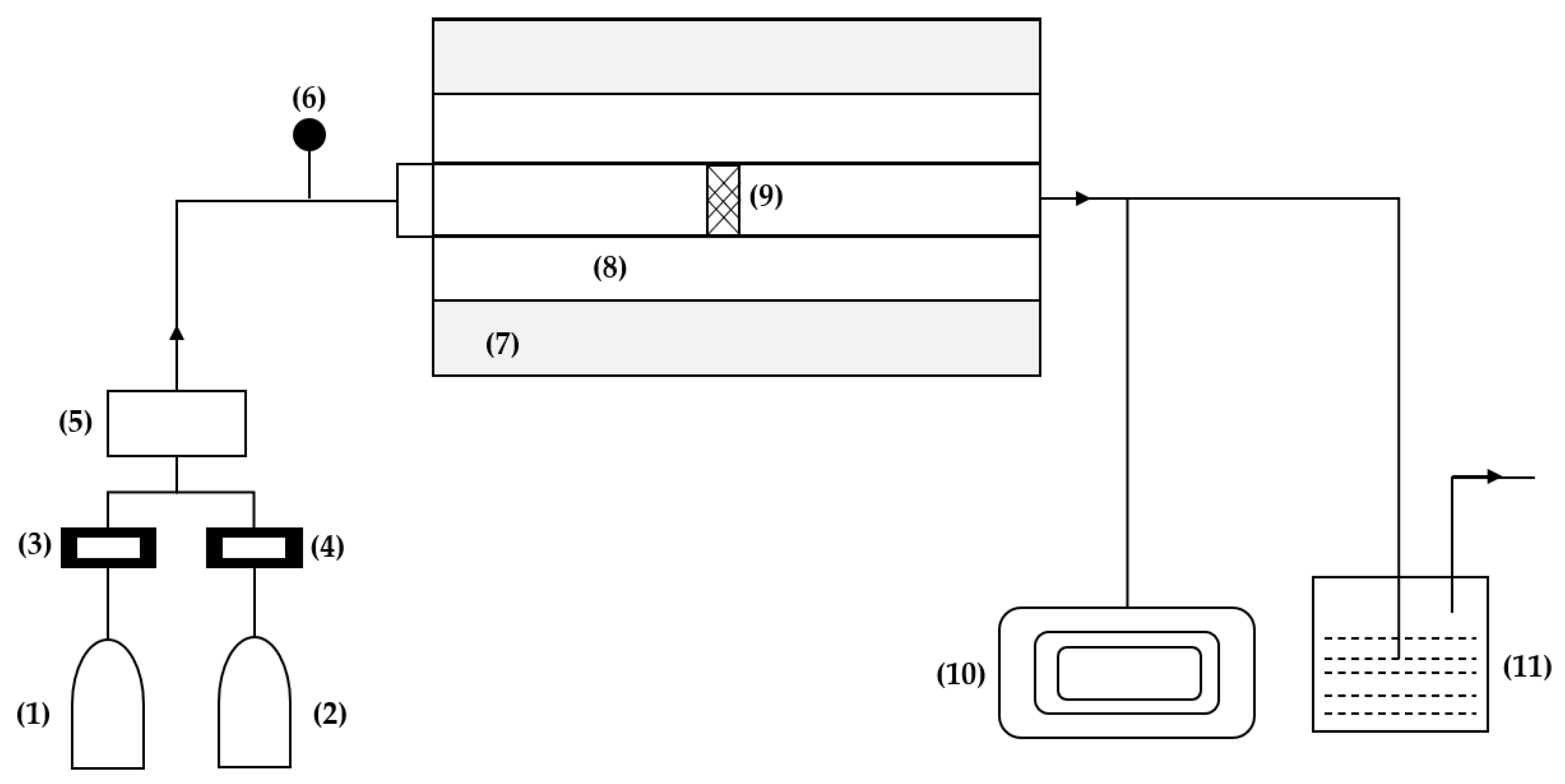
Figure 4. Experimental deposition system: (1) argon, (2) propylene, (3) flow meter, (4) manometer, (5) mixing cylinder, (6) manometer, (7) furnace, (8) graphite reaction chamber, (9) carbon layer, (10) vacuum pump, (11) off-gas treatment device.
3.3. Electrophoretic Deposition
Electrophoretic deposition is a widely used technique that promises cost-effective deposition of nanoparticles with relevant applications, such as obtaining antibacterial properties and improving the biocompatibility of a ceramic compound. It is used to uniformly coat an electrode immersed in a stable suspension. The cathode and anode are subjected to an electric field, inducing the movement of precursor particles to the substrate [47][37]. The electrophoretic deposition can be applied to ceramic, metal, and polymer substrates. Figure 5 illustrates the setup used by Huanyu Li et al. [40][38] for electrophoretic deposition, where doping of nano-silica onto carbon fibers is performed. A carbon fiber anode is immersed in distilled water containing nano-silica colloids, and a graphite cylinder is used as the counter electrode. In this technique, voltage and time parameters can be varied, typically ranging from 0 V to 3 V throughout 0 to 15 min, depending on the desired doping, followed by drying of the specimens.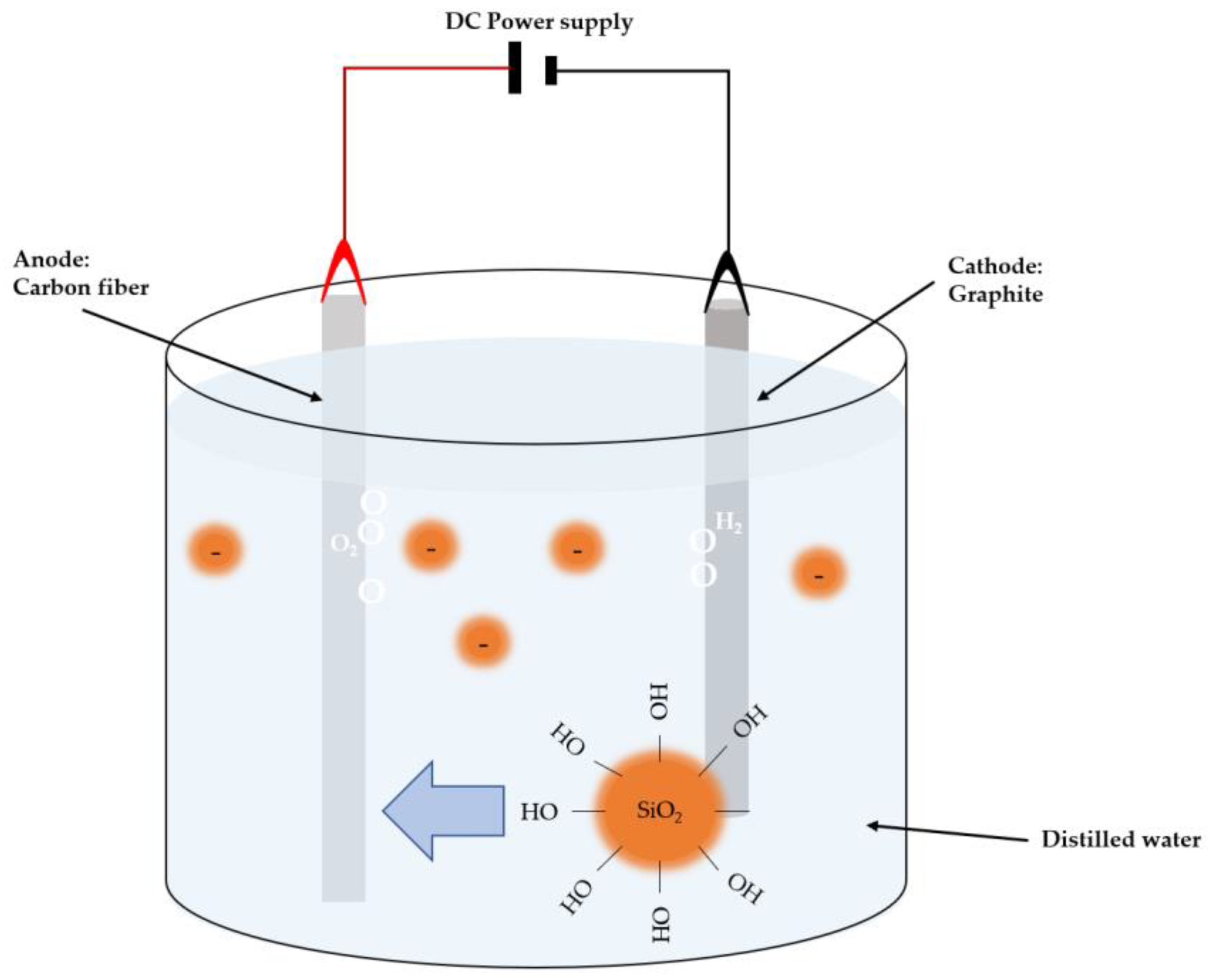
Figure 5. Schematic illustration of EPD configuration for CF surface modification.
4. Deposition of Nanomaterials on Metallic Substrates
The functionalization of metallic substrates has allowed for new applications of these materials in optical, medical, environmental, and other fields. These substrates exhibit different mechanical, optical, electrical, catalytic, and magnetic properties depending on the type of nanoparticle used for functionalization.4.1. Laser Metal Deposition
This technique is mainly based on a fiber laser with a power of ~6000 W that irradiates the substrate while directing the powder of the desired doping material, including metal, ceramic and polymer substrates. Figure 6 shows the laser metal deposition (LMD) process diagram. This technique provides high precision and a rapid deposition rate [48][43].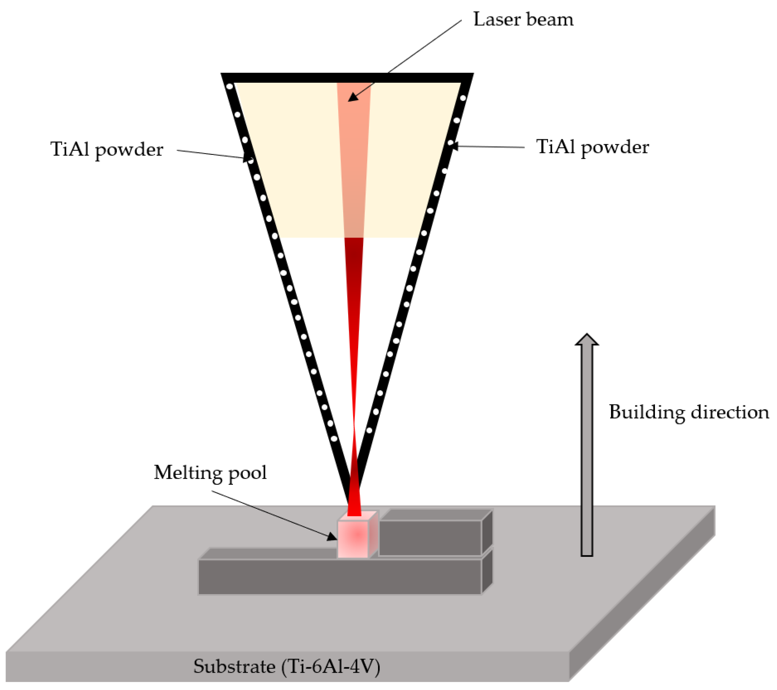
Figure 6. Schematic illustration of the LMD process.
4.2. Electrochemical Deposition
Electrochemical deposition is similar to electrophoretic deposition as it occurs in an electrochemical cell. It is carried out using different configurations with electrodes submerged in an electrolyte mixed with the precursor, which is then subjected to a voltage to induce doping. In the study by C. Augello et al. [50][45], the substrate was immersed in a solution of monomers acting as precursors. When the voltage was applied, the monomers underwent chemical polymerization on the substrate. This method offers advantages such as improving the interfacial bond between the coating material and the substrate.4.3. Atomic Layer Deposition (ALD)
ALD is a particular variant of the CVD technique. In ALD, gas-phase reactants are also introduced into a reaction chamber to form the desired material through surface chemical reactions. The difference is that, in ALD, the precursors are pulsed alternately, one at a time, with an intermediate purge of inert gas [51][46]. This technique is based on sequential and self-limiting surface reactions. Most ALD processes involve binary reaction sequences where two surface reactions occur to form the layer. This method offers advantages such as precise control over film thickness and can be applied to metal and ceramic substrates [52][47]. In the study by Sheng-Hao et al. [53][48], the substrate was deposited in a commercial ALD system with the precursor and H2O at a chamber temperature of 200 °C. The precursor container was heated to 70 °C, and the H2O container was kept at room temperature during the ALD processing. A cycle consisted of six steps: precursor 1/dosing time, soak time, evacuation time; precursor 2/dosing time, soak time. During ALD processing, there is a constant flow of carrier gas. Furthermore, chemical vapor deposition of carbon nano-onions on Fe/Fe3C matrices offers corrosion protection, while atomic layer deposition of nano Sn–O2 on titanium demonstrates biocompatibility. Laser metal deposition with nano-SiCp on AlSi10Mg alloy influenced the microstructure, decreasing SiCp size and intensifying the reaction between SiC and the aluminum matrix. Other notable findings include electrophoretic deposition of chitosan-reinforced Baghdadite ceramic nanoparticles on stainless steel 316 L to improve biological and physical characteristics, electrophoretic deposition of polyaniline (PANI) nanofibers on copper for corrosion protection, and in situ deposition of Pt nanoparticles on nanopore stainless steel for high active hydrogen evolution reaction. These findings contribute to a comprehensive understanding of nanomaterial deposition techniques and their potential applications, facilitating the development of advanced materials with tailored properties in nanotechnology. The CVD stands out as an economical and effective alternative for the deposition of nanomaterials. It allows for the modification of different materials by providing nanostructures on their surface. For example, nitride semiconductors like gallium nitrides and aluminum nitrides can be produced using CVD, forming nanostructures known as quantum confinement points. These nanostructures allow the materials to be utilized in a wide range of optical and microelectronic devices [87][49].References
- Leong, C.Y.; Wahab, R.A.; Lee, S.L.; Ponnusamy, V.K.; Chen, Y.-H. Current Perspectives of Metal-Based Nanomaterials as PhotocatalyticPhotocatalytic Antimicrobial Agents and Their Therapeutic Modes of Action: A Review. Environ. Res. 2023, 227, 115578.
- Bratovcic, A. Different Applications of Nanomaterials and Their Impact on the Environment. Int. J. Mater. Sci. Eng. 2019, 5, 1–7.
- Laux, P.; Riebeling, C.; Booth, A.M.; Brain, J.D.; Brunner, J.; Cerrillo, C.; Creutzenberg, O.; Estrela-Lopis, I.; Gebel, T.; Johanson, G.; et al. Biokinetics of Nanomaterials: The Role of Biopersistence. NanoImpact 2017, 6, 69–80.
- Gaffet, E. Nanomaterials: A Review of the Definitions, Applications, Health Effects. Available online: https://arxiv.org/abs/1106.2206 (accessed on 9 July 2023).
- Allied Market Research Nanomaterials Market Research 2031. Available online: https://www.alliedmarketresearch.com/nano-materials-market (accessed on 9 July 2023).
- Future Market Insights Nanomaterials Market to Exceed a Valuation of US$ 45 Billion by 2032 Attributing to Its Rising Use in Healthcare and Automotive Sectors. Available online: https://finance.yahoo.com/news/nanomaterials-market-exceed-valuation-us-150000849.html (accessed on 10 July 2023).
- Future Market Insights Nanomaterials Market. Available online: https://www.futuremarketinsights.com/reports/nanomaterials-market (accessed on 10 July 2023).
- Patra, J.K.; Baek, K.-H. Green Nanobiotechnology: Factors Affecting Synthesis and Characterization Techniques. J. Nanomater. 2014, 2014, 417305.
- Govindaraman, L.T.; Arjunan, A.; Baroutaji, A.; Robinson, J.; Ramadan, M.; Olabi, A.-G. Nanomaterials Theory and Applications. In Encyclopedia of Smart Materials; Elsevier: Amsterdam, The Netherlands, 2022; pp. 302–314.
- Saleh, T.A. Nanomaterials for Pharmaceuticals Determination. Bioenergetics 2016, 5, 1000226.
- Jeyaraj, M.; Gurunathan, S.; Qasim, M.; Kang, M.-H.; Kim, J.-H. A Comprehensive Review of the Synthesis, Characterization, and Biomedical Application of Platinum Nanoparticles. Nanomaterials 2019, 9, 1719.
- Li, X.; Zhou, Y.; Li, L.; Wang, T.; Wang, B.; Che, R.; Zhai, Y.; Zhang, J.; Li, W. Metal Selenide Nanomaterials for Biomedical Applications. Colloids Surf. B Biointerfaces 2023, 225, 113220.
- European Commission Internal Market, Industry, Entrepreneurship and SMEs: Nanomaterials. Available online: https://single-market-economy.ec.europa.eu/sectors/chemicals/reach/nanomaterials_en (accessed on 10 July 2023).
- Grand View Research Nanomaterials Market Size, Share & Growth. Available online: https://www.grandviewresearch.com/industry-analysis/nanotechnology-and-nanomaterials-market (accessed on 10 July 2023).
- Bondavalli, P.; Pribat, D.; Legagneux, P.; Martin, M.-B.; Hamidouche, L.; Qassym, L.; Feugnet, G.; Trompeta, A.-F.; Charitidis, C.A. Deposition of Graphene and Related Nanomaterials by Dynamic Spray-Gun Method: A New Route to Implement Nanomaterials in Real Applications. J. Phys. Mater. 2019, 2, 032002.
- Harish, V.; Ansari, M.M.; Tewari, D.; Gaur, M.; Yadav, A.B.; García-Betancourt, M.-L.; Abdel-Haleem, F.M.; Bechelany, M.; Barhoum, A. Nanoparticle and Nanostructure Synthesis and Controlled Growth Methods. Nanomaterials 2022, 12, 3226.
- Chaudhary, P.; Fatima, F.; Kumar, A. Relevance of Nanomaterials in Food Packaging and Its Advanced Future Prospects. J. Inorg. Organomet. Polym. Mater. 2020, 30, 5180–5192.
- Yoo, H.; Heo, K.; Ansari, M.H.R.; Cho, S. Recent Advances in Electrical Doping of 2D Semiconductor Materials: Methods, Analyses, and Applications. Nanomaterials 2021, 11, 832.
- Diop, M.M.; Diaw, A.; Mbengue, N.; Ba, O.; Diagne, M.; Niasse, O.A.; Ba, B.; Sarr, J. Optimization and Modeling of Antireflective Layers for Silicon Solar Cells: In Search of Optimal Materials. Mater. Sci. Appl. 2018, 9, 705–722.
- Chen, Y.; Fan, S.W.; Gao, G.Y. Design Ambipolar Conductivity on Wide-Gap Semiconductors: The Case of Al- and Na-Doped CaS. Mater. Sci. Semicond. Process. 2022, 151, 107024.
- Aghababai Beni, A.; Jabbari, H. Nanomaterials for Environmental Applications. Results Eng. 2022, 15, 100467.
- Wu, Q.; Miao, W.; Zhang, Y.; Gao, H.; Hui, D. Mechanical Properties of Nanomaterials: A Review. Nanotechnol. Rev. 2020, 9, 259–273.
- Pokropivny, V.; Lohmus, R.; Hussainova, I.; Pokropivny, A.; Vlassov, S. Introduction in Nanomaterials and Nanotechnology, 1st ed.; University of Tartu, Ed.; University of Tartu: Tartu, Estonia, 2007; Volume 1.
- Dorval Dion, C.A.; Tavares, J.R. Photo-Initiated Chemical Vapor Deposition as a Scalable Particle Functionalization Technology: A Practical Review. Powder Technol. 2013, 239, 484–491.
- Darghlou, S.J.; Kangarlou, H.; Razzazi, V. Effect of Vertical Deposition Angle on Structural and Optical Properties of Tantalum Oxide Nano Layers Deposited by Electron Gun Evaporation. Chin. J. Phys. 2021, 74, 226–238.
- Nagi, C.S.; Ogin, S.L.; Mohagheghian, I.; Crean, C.; Foreman, A.D. Spray Deposition of Graphene Nanoplatelets for Modifying Interleaves in Carbon Fibre Reinforced Polymer Laminates. Mater. Des. 2020, 193, 108831.
- Zhang, S.; Zhang, W.; Lu, G. Ordered ZnO Nanorod Array Films Prepared by Low Cost Electrochemical Deposition and Its Optical Properties. Mater. Lett. 2015, 138, 262–264.
- Jiang, H.; Manolache, S.; Wong, A.C.L.; Denes, F.S. Plasma-Enhanced Deposition of Silver Nanoparticles onto Polymer and Metal Surfaces for the Generation of Antimicrobial Characteristics. J. Appl. Polym. Sci. 2004, 93, 1411–1422.
- Bruno, L.; Urso, M.; Shacham-Diamand, Y.; Priolo, F.; Mirabella, S. Role of Substrate in Au Nanoparticle Decoration by Electroless Deposition. Nanomaterials 2020, 10, 2180.
- Wang, Z.; Zhang, Z. Electron Beam Evaporation Deposition. In Advanced Nano Deposition Methods; Chemical Industry Press: Beijing, China, 2016; pp. 33–58.
- Makhlouf, A.S.H. Current and Advanced Coating Technologies for Industrial Applications. In Nanocoatings and Ultra-Thin Films; Woodhead Publishing Ltd.: Cambridge, UK, 2011; pp. 3–23.
- Saravanavel, G.; Honnali, S.K.; Lourdes, K.S.; John, S.; Gunasekhar, K.R. Study on the Thermoelectric Properties of Al-ZnO Thin-Film Stack Fabricated by Physical Vapour Deposition Process for Temperature Sensing. Sens. Actuators A Phys. 2021, 332, 113097.
- Albu, C.; Eremia, S.A.V.; Veca, M.L.; Avram, A.; Popa, R.C.; Pachiu, C.; Romanitan, C.; Kusko, M.; Gavrila, R.; Radoi, A. Dataset on Large Area Nanocrystalline Graphite Film (NCG) Grown on SiO2 Using Plasma-Enhanced Chemical Vapour Deposition. Data Brief 2019, 24, 103923.
- Said, N.; Khoo, Y.S.; Lau, W.J.; Gürsoy, M.; Karaman, M.; Ting, T.M.; Abouzari-Lotf, E.; Ismail, A.F. Rapid Surface Modification of Ultrafiltration Membranes for Enhanced Antifouling Properties. Membranes 2020, 10, 401.
- Karabiberoğlu, Ş.; Dursun, Z. Au-Pt Bimetallic Nanoparticles Anchored on Conducting Polymer: An Effective Electrocatalyst for Direct Electrooxidation of Sodium Borohydride in Alkaline Solution. Mater. Sci. Eng. B 2023, 288, 116158.
- Kun, H.; Li, J.; Li, K.; Yan, N.; Bian, C.; Guan, Y.; Yang, Y.; Li, H. Effects of Temperature and Pressure on Chemical Vapour Deposition in Micro-Nano Porous Structure in Char Layer of Polymer Composites. Polym. Degrad. Stab. 2022, 196, 109816.
- Thinakaran, S.; Loordhuswamy, A.M.; Venkateshwapuram Rengaswami, G.D. Electrophoretic Deposition of Chitosan/Nano Silver Embedded Micro Sphere on Centrifugal Spun Fibrous Matrices—A Facile Biofilm Resistant Biocompatible Material. Int. J. Biol. Macromol. 2020, 148, 68–78.
- Li, H.; Liebscher, M.; Curosu, I.; Choudhury, S.; Hempel, S.; Davoodabadi, M.; Dinh, T.T.; Yang, J.; Mechtcherine, V. Electrophoretic Deposition of Nano-Silica onto Carbon Fiber Surfaces for an Improved Bond Strength with Cementitious Matrices. Cem. Concr. Compos. 2020, 114, 103777.
- Zhou, X.; Yin, A.; Sheng, J.; Wang, J.; Chen, H.; Fang, Y.; Zhang, K. In Situ Deposition of Nano Cu2O on Electrospun Chitosan Nanofibrous Scaffolds and Their Antimicrobial Properties. Int. J. Biol. Macromol. 2021, 191, 600–607.
- Pooyandeh, S.; Shahidi, S.; Khajehnezhad, A.; Mongkholrattanasit, R. In Situ Deposition of NiO Nano Particles on Cotton Fabric Using Sol–Gel Method- PhotocatalyticPhotocatalytic Activation Properties. J. Mater. Res. Technol. 2021, 12, 1–14.
- Menazea, A.A.; Abdelbadie, S.A.; Ahmed, M.K. Manipulation of AgNPs Coated on Selenium/Carbonated Hydroxyapatite/ε-Polycaprolactone Nanofibrous via Pulsed Laser Deposition for Wound Healing Applications. Appl. Surf. Sci. 2020, 508, 145299.
- Li, Z.S.; Lin, S.; Chen, Z.L.; Shi, Y.D.; Huang, X.M. In Situ Electro-Deposition of Pt Micro-Nano Clusters on the surface of {3−/PAMAM}n Multilayer Composite Films and Their Electrocatalytic Activities Regarding Methanol Oxidation. J. Colloid Interface Sci. 2012, 368, 413–419.
- Zhai, W.; Wu, N.; Zhou, W. Laser Metal Deposition of Low Carbon 410L Stainless Steel and Heat Treatment. Mater. Sci. Eng. A 2023, 872, 144987.
- Zhang, Q.; Sun, W.; Xu, S.; Zhang, X.; Wang, J.; Si, C. Nano-TiB Whiskers Reinforced Ti–6Al–4 V Matrix Composite Fabricated by Direct Laser Deposition: Microstructure and Mechanical Properties. J. Alloys Compd. 2022, 922, 166171.
- Augello, C.; Liu, H. Surface Modification of Magnesium by Functional Polymer Coatings for Neural Applications. Surf. Modif. Magnes. Its Alloys Biomed. Appl. 2015, 2, 335–353.
- Leskelä, M.; Niinistö, J.; Ritala, M. Atomic Layer Deposition. Compr. Mater. Process. 2014, 4, 101–123.
- George, S.M. Atomic Layer Deposition: An Overview. Chem. Rev. 2010, 110, 111–131.
- Hsu, S.-H.; Liao, H.-T.; Chen, R.-S.; Chiu, S.-C.; Tsai, F.-Y.; Lee, M.-S.; Hu, C.-Y.; Tseng, W.-Y. The Influence on Surface Characteristic and Biocompatibility of Nano-SnO2-Modified Titanium Implant Material Using Atomic Layer Deposition Technique. J. Formos. Med. Assoc. 2022, 122, 230–238.
- Bouchkour, Z.; Tristant, P.; Thune, E.; Dublanche-Tixier, C.; Jaoul, C.; Guinebretière, R. Aluminum Nitride Nano-Dots Prepared by Plasma Enhanced Chemical Vapor Deposition on Si(111). Surf. Coat. Technol. 2011, 205, S586–S591.
More