Perovskite solar cells (PSCs) have revolutionized the field of photovoltaics, achieving certified power conversion efficiencies reaching 26% at the laboratory scale. High performance, enhanced stability, and long lifetime are prerequisites for the industrialization and commercialization of this class of third-generation photovoltaic technology. The electron transport layer (ETL) plays a pivotal role in obtaining stable perovskite solar cells with a high power conversion efficiency (PCE). It must be characterized by high transparency to visible light, photostability, and compatibility with the perovskite used. Therefore, a thorough comprehension and optimization of the interaction between perovskite materials and TiO2 ETL underlayers, as well as a special focus on the behavior of the corresponding devices, are necessary.
- perovskite solar cells
- perovskite interface
- electron transport layer
1. Introduction
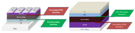
2. Functionalization of ETL/Perovskite Interface
References
- Saliba, M.; Matsui, T.; Domanski, K.; Seo, J.-Y.; Ummadisingu, A.; Zakeeruddin, S.M.; Correa-Baena, J.-P.; Tress, W.R.; Abate, A.; Hagfeldt, A.; et al. Incorporation of rubidium cations into perovskite solar cells improves photovoltaic performance. Science 2016, 354, 206–209.
- Li, Z.; Li, B.; Wu, X.; Sheppard, S.A.; Zhang, S.; Gao, D.; Long, N.J.; Zhu, Z. Organometallic-Functionalized Interfaces for Highly Efficient Inverted Perovskite Solar Cells. Science 2022, 376, 416–420.
- Chen, C.-I.; Wu, S.; Lu, Y.-A.; Lee, C.-C.; Ho, K.-C.; Zhu, Z.; Chen, W.-C.; Chueh, C.-C. Enhanced Near-Infrared Photoresponse of Inverted Perovskite Solar Cells Through Rational Design of Bulk-Heterojunction Electron-Transporting Layers. Adv. Sci. 2019, 6, 1901714.
- Rong, Y.; Hu, Y.; Mei, A.; Tan, H.; Saidaminov, M.I.; Seok, S.I.; McGehee, M.D.; Sargent, E.H.; Han, H. Challenges for Commercializing Perovskite Solar Cells. Science 2018, 361, 1214.
- Correa-Baena, J.P.; Saliba, M.; Buonassisi, T.; Grätzel, M.; Abate, A.; Tress, W.; Hagfeldt, A. Promises and Challenges of Perovskite Solar Cells. Science 2017, 358, 739–744.
- Stranks, S.; Snaith, H.J. Metal-halide perovskites for photovoltaic and light-emitting devices. Nat. Nanotechnol. 2015, 10, 391–402.
- Zheng, X.; Chen, B.; Dai, J.; Fang, Y.; Bai, Y.; Lin, Y.; Wei, H.; Zeng, X.C.; Huang, J. Defect passivation in hybrid perovskite solar cells using quaternary ammonium halide anions and cations. Nat. Energy 2017, 2, 17102.
- Chen, J.; Park, N.-G. Materials and Methods for Interface Engineering toward Stable and Efficient Perovskite Solar Cells. ACS Energy Lett. 2020, 5, 2742–2786.
- Shao, Y.; Yuan, Y.; Huang, J. Correlation of energy disorder and open-circuit voltage in hybrid perovskite solar cells. Nat. Energy 2016, 1, 15001–15006.
- Bu, T.; Li, J.; Zheng, F.; Chen, W.; Wen, X.; Ku, Z.; Peng, Y.; Zhong, J.; Cheng, Y.-B.; Huang, F. Universal passivation strategy to slot-die printed SnO2 for hysteresis-free efficient flexible perovskite solar module. Nat. Commun. 2018, 9, 4609.
- Yang, D.; Yang, R.; Wang, K.; Wu, C.; Zhu, X.; Feng, J.; Ren, X.; Fang, G.; Priya, S.; Liu, S.F. High efficiency planar-type perovskite solar cells with negligible hysteresis using EDTA-complexed SnO2. Nat. Commun. 2018, 9, 3239.
- Yun, A.J.; Kim, J.; Hwang, T.; Park, B. Origins of Efficient Perovskite Solar Cells with Low-Temperature Processed SnO2 Electron Transport Layer. ACS Appl. Energy Mater. 2019, 2, 3554–3560.
- Luo, D.; Yang, W.; Wang, Z.; Sadhanala, A.; Hu, Q.; Su, R.; Shivanna, R.; Trindade, G.F.; Watts, J.F.; Xu, Z.; et al. Enhanced photovoltage for inverted planar heterojunction perovskite solar cells. Science 2018, 360, 1442–1446.
- Raiford, J.A.; Belisle, R.A.; Bush, K.A.; Prasanna, R.; Palmstrom, A.F.; McGehee, M.D.; Bent, S.F. Atomic layer deposition of vanadium oxide to reduce parasitic absorption and improve stability in n–i–p perovskite solar cells for tandems. Sustain. Energy Fuels 2019, 3, 1517–1525.
- Kamat, P.V.; Kuno, M. Halide Ion Migration in Perovskite Nanocrystals and Nanostructures. Acc. Chem. Res. 2021, 54, 520–531.
- Ricciarelli, D.; Kaiser, W.; Mosconi, E.; Wiktor, J.; Ashraf, M.W.; Malavasi, L.; Ambrosio, F.; De Angelis, F. Reaction Mechanism of Photocatalytic Hydrogen Production at Water/Tin Halide Perovskite Interfaces. ACS Energy Lett. 2022, 7, 1308–1315.
- Shin, S.S.; Lee, S.J.; Seok, S.I. Metal Oxide Charge Transport Layers for Efficient and Stable Perovskite Solar Cells. Adv. Funct. Mater. 2019, 29, 1900455.
- Xing, G.; Wu, B.; Chen, S.; Chua, J.; Yantara, N.; Mhaisalkar, S.; Mathews, N.; Sum, T.C. Interfacial Electron Transfer Barrier at Compact TiO2/CH3NH3PbI3 Heterojunction. Small 2015, 11, 3606.
- Jung, K.; Lee, J.; Im, C.; Do, J.; Kim, J.; Chae, W.-S.; Lee, M.-J. Highly Efficient Amorphous Zn2SnO4 Electron-Selective Layers Yielding over 20% Efficiency in FAMAPbI3-Based Planar Solar Cells. ACS Energy Lett. 2018, 3, 2410–2417.
- Zhong, Y.; Hufnagel, M.; Thelakkat, M.; Li, C.; Huettner, S. Role of PCBM in the Suppression of Hysteresis in Perovskite Solar Cells. Adv. Funct. Mater. 2020, 30, 1908920.
- Hussain, S.; Liu, H.L.; Vikraman, D.; Jaffery, S.H.A.; Nazir, G.; Shahzad, F.; Batoo, K.M.; Jung, J.W.; Kang, J.W.; Kim, H.-S. Tuning of electron transport layers using MXene/metal-oxide nanocomposites for perovskite solar cells and X-ray detectors. Nanoscale 2023, 15, 7329–7343.
- Jiang, Y.; Wang, J.; Zai, H.; Ni, D.; Wang, J.; Xue, P.; Li, N.; Jia, B.; Lu, H.; Zhang, Y.; et al. Reducing Energy Disorder in Perovskite Solar Cells by Chelation. J. Am. Chem. Soc. 2022, 144, 5400–5410.
- Wang, C.; Yang, H.; Xia, X.; Wang, X.; Li, F. Suppressing interfacial defect formation derived from in-situ-generated polyethylenimine-based 2D perovskites to boost the efficiency and stability NiOx-based inverted planar perovskite solar cells. Appl. Surf. Sci. 2021, 548, 149276.
- Ho, I.-H.; Huang, Y.-J.; Cai, C.-E.; Liu, B.-T.; Wu, T.-M.; Lee, R.-H. Enhanced Photovoltaic Performance of Inverted Perovskite Solar Cells through Surface Modification of aNiOx-Based Hole-Transporting Layer with Quaternary Ammonium Halide–Containing Cellulose Derivatives. Polymers 2023, 15, 437.
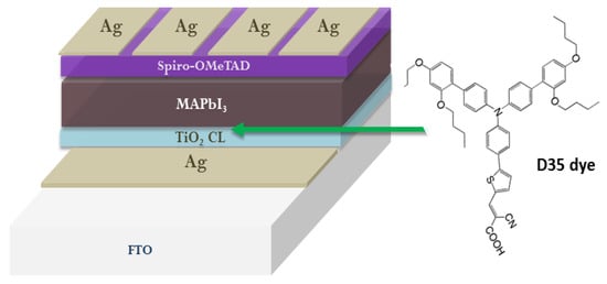
- Balis, N.; Zaky, A.A.; Perganti, D.; Kaltzoglou, A.; Sygellou, L.; Katsaros, F.; Stergiopoulos, T.; Kontos, A.G.; Falaras, P. Dye Sensitization of Titania Compact Layer for Efficient and Stable Perovskite Solar Cells. ACS Appl. Energy Mater. 2018, 1, 6161–6171.
- Zaky, A.A.; Balis, N.; Gkini, K.; Athanasekou, C.; Kaltzoglou, A.; Stergiopoulos, T.; Falaras, P. Dye Engineered Perovskite Solar Cells under Accelerated Thermal Stress and Prolonged Light Exposure. ChemistrySelect 2020, 5, 4454–4462.
- Chouk, R.; Haouanoh, D.; Aguir, C.; Bergaoui, M.; Toubane, M.; Bensouici, F.; Tala-Ighil, R.; Erto, A.; Khalfaoui, M. Dye Sensitized TiO2 and ZnO Charge Transport Layers for Efficient Planar Perovskite Solar Cells: Experimental and DFT Insights. J. Electron. Mater. 2020, 49, 1396–1403.
- Noh, Y.W.; Lee, J.H.; Jin, I.S.; Park, S.H.; Jung, J.W. Enhanced efficiency and ambient stability of planar heterojunction perovskite solar cells by using organic-inorganic double layer electron transporting material. Electrochim. Acta 2019, 294, 337–344.
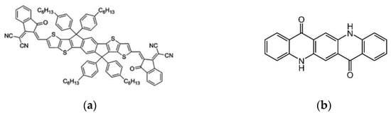
- Qi, Y.; Ndaleh, D.; Meador, W.E.; Delcamp, J.H.; Hill, G.; Pradhan, N.R.; Dai, Q. Interface Passivation of Inverted Perovskite Solar Cells by Dye Molecules. ACS Appl. Energy Mater. 2021, 4, 9525–9533.
- He, Q.; Worku, M.; Liu, H.; Lochner, E.; Robb, A.J.; Lteif, S.; Raaj, J.S.; Winfred, V.; Hanson, K.; Schlenoff, J.B.; et al. Highly Efficient and Stable Perovskite Solar Cells Enabled by Low Cost Industrial Organic Pigment. Angew. Chem. Int. Ed. 2021, 60, 2485.
- Mahmud, M.A.; Elumalai, N.K.; Upama, M.B.; Wang, D.; Ales, V.G. Cesium compounds as interface modifiers for stable and efficient perovskite solar cells. Sol. Energy Mater. Sol. Cells 2018, 174, 172–186.
- Ruankham, P.; Wongratanaphisan, D.; Gardchareon, A.; Phadungdhitidhada, S.; Choopun, S.; Sagawa, T. Full coverage of perovskite layer onto ZnO nanorods via a modified sequential two-step deposition method for efficiency enhancement in perovskite solar cells. Appl. Surf. Sci. 2017, 410, 393–400.
- Zhang, P.; Wu, J.; Zhang, T.; Wang, Y.; Liu, D.; Chen, H.; Ji, L.; Liu, C.; Ahmad, W.; Chen, Z.D.; et al. Perovskite solar cells with ZnO electron-transporting materials. Adv. Mater. 2018, 30, 1703737.
- Huang, A.; Lei, L.; Zhu, J.; Yu, Y.; Liu, Y.; Yang, S.; Bao, S.; Jin, P. Controllable deposition of TiO2 nanopillars at room temperature for high performance perovskite solar cells with suppressed hysteresis. Sol. Energy Mater. Sol. Cells 2017, 168, 172–182.
- Huang, X.; Hu, Z.; Xu, J.; Wang, P.; Wang, L.; Zhang, J.; Zhu, Y. Low-temperature processed SnO2 compact layer by incorporating TiO2 layer toward efficient planar heterojunction perovskite solar cells. Sol. Energy Mater. Sol. Cells 2017, 164, 87–92.
- Ren, X.; Yang, D.; Yang, Z.; Feng, J.; Zhu, X. Solution-processed Nb: SnO2 electron transport layer for efficient planar perovskite solar cells. ACS Appl. Mater. Interfaces 2017, 9, 2421–2429.
- Song, J.; Zheng, E.; Bian, J.; Wang, X.; Tian, W.; Sanehira, Y.; Miyasaka, T. Low temperature SnO2-based electron selective contact for efficient and stable perovskite solar cells. J. Mater. Chem. A. 2015, 3, 10837–10844.
- Eze, V.O.; Seike, Y.; Mori, T. Efficient planar perovskite solar cells using solution processed amorphous WOx/fullerene C60 as electron extraction layers. Org. Electron. 2017, 46, 253–262.
- Pintilie, I.; Stancu, V.; Tomulescu, A.; Radu, R.; Besleaga Stan, C.; Trinca, L.; Pintilie, L. Properties of perovskite ferroelectrics deposited on F doped SnO2 electrodes and the prospect of their integration into perovskite solar cells. Mater. Des. 2017, 135, 112–121.
- Eperon, G.E.; Burlakov, V.M.; Docampo, P.; Goriely, A.; Snaith, H.J. Morphological Control for High Performance, Solution Processed Planar Heterojunction Perovskite Solar Cells. Adv. Funct. Mater. 2014, 24, 151–157.
- Sun, S.Y.; Salim, T.; Mathews, N.; Duchamp, M.; Boothroyd, C.; Xing, G.C.; Sum, T.C.; Lam, Y.M. The origin of high efficiency in low-temperature solution-processable bilayer organometal halide hybrid solar cells. Energy Environ. Sci. 2014, 7, 399–407.
- Wu, M.C.; Chan, S.H.; Jao, M.H.; Su, W.F. Enhanced short-circuit current density of perovskite solar cells using Zn-doped TiO2 as electron transport layer. Sol. Energy Mater. Sol. Cells 2016, 157, 447–453.
- Wojciechowski, K.; Fang, S.D.; Abate, A.; Sadoughi, G.; Sadhanala, A.; Kopidakis, N.; Rumbles, G.; Li, C.Z.; Friend, R.H.; Jen, A.K.Y.; et al. Heterojunction Modification for Highly Efficient Organic-Inorganic Perovskite Solar Cells. ACS Nano 2014, 8, 12701–12709.
- Heo, J.H.; Han, H.J.; Kim, D.; Ahn, T.K.; Im, S.H. Hysteresis-less inverted CH3NH3PbI3 planar perovskite hybrid solar cells with 18.1% power conversion efficiency. Energy Environ. Sci. 2015, 8, 1602–1608.
- Murugadoss, G.; Tanaka, S.; Mizuta, G.; Kanaya, S.; Nishino, H.; Umeyama, T.; Imahori, H.; Ito, S. Light stability tests of methylammonium and formamidinium Pb-halide perovskite for solar cell applications. Jpn. J. Appl. Phys. 2015, 54, 08KF08.
- Zhou, H.; Chen, Q.; Li, G.; Luo, S.; Song, T.-B.; Duan, H.-S.; Hong, Z.; You, J.; Liu, Y.; Yang, Y. Interface engineering of highly efficient perovskite solar cells. Science 2014, 345, 542–546.
- Sidhik, S.; Cerdan Pasarán, A.; Esparza, D.; López Luke, T.; Carriles, R.; De la Rosa, E. Improving the optoelectronic properties of mesoporous TiO2 by cobalt doping for high-performance hysteresis-free perovskite solar cells. ACS Appl. Mater. Interfaces 2018, 10, 3571–3580.
- Giordano, F.; Abate, A.; Correa Baena, J.P.; Saliba, M.; Matsui, T.; Im, S.H.; Zakeeruddin, S.M.; Nazeeruddin, M.K.; Hagfeldt, A.; Graetzel, M. Enhanced electronic properties in mesoporous TiO2 via lithium doping for high-efficiency perovskite solar cells. Nat. Commun. 2016, 7, 10379.
- Ranjitha, A.; Thambidurai, M.; Shini, F.; Muthukumarasamy, N.; Velauthapillai, D. Effect of doped TiO2 film as electron transport layer for inverted organic solar cell. Mater. Sci. Energy Technol. 2019, 2, 385–388.
- Su, T.-S.; Wei, T.-C. Co-Electrodeposition of Sn-Doped TiO2 Electron-Transporting Layer for Perovskite Solar Cells. Phys. Status Solidi A 2020, 217, 1900491.
- Wu, T.; Zhen, C.; Zhu, H.; Wu, J.; Jia, C.; Wang, L.; Liu, G.; Park, N.-G.; Cheng, H.-M. Gradient Sn-Doped Heteroepitaxial Film of Faceted Rutile TiO2 as an Electron Selective Layer for Efficient Perovskite Solar Cells. ACS Appl. Mater. Interfaces 2019, 11, 19638–19646.
- Gu, X.; Wang, Y.; Zhang, T.; Liu, D.; Zhang, R.; Zhang, P.; Wu, J.; Chen, Z.D.; Li, S. Enhanced electronic transport in Fe3+-doped TiO2 for high efficiency perovskite solar cells. J. Mater. Chem. C 2017, 5, 10754–10760.
- Xu, Z.; Yin, X.; Guo, Y.; Pu, Y.; He, M. Ru-Doping in TiO2 electron transport layers of planar heterojunction perovskite solar cells for enhanced performance. J. Mater. Chem. C 2018, 6, 4746–4752.
- Wang, S.; Liu, B.; Zhu, Y.; Ma, Z.; Liu, B.; Miao, X.; Ma, R.; Wang, C. Enhanced performance of TiO2-based perovskite solar cells with Ru-doped TiO2 electron transport layer. Sol. Energy 2018, 169, 335–342.
- Chen, B.-X.; Rao, H.-S.; Li, W.-G.; Xu, Y.-F.; Chen, H.-Y.; Kuang, D.-B.; Su, C.-Y. Achieving high-performance planar perovskite solar cell with Nb-doped TiO2 compact layer by enhanced electron injection and efficient charge extraction. J. Mater. Chem. A 2016, 4, 5647–5653.
- Wu, M.-C.; Chan, S.-H.; Lee, K.-M.; Chen, S.-H.; Jao, M.-H.; Chen, Y.-F.; Su, W.-F. Enhancing the efficiency of perovskite solar cells using mesoscopic zinc-doped TiO2 as the electron extraction layer through band alignment. J. Mater. Chem. A 2018, 6, 16920–16931.
- Lv, M.; Lv, W.; Fang, X.; Sun, P.; Lin, B.; Zhang, S.; Xu, X.; Ding, J.; Yuan, N. Performance enhancement of perovskite solar cells with a modified TiO2 electron transport layer using Zn-based additives. RSC Adv. 2016, 6, 35044–35050.
- Ranjan, R.; Prakash, A.; Singh, A.; Singh, A.; Garg, A.; Gupta, R.K. Effect of tantalum doping in a TiO2 compact layer on the performance of planar spiro-OMeTAD free perovskite solar cells. J. Mater. Chem. A 2018, 6, 1037–1047.
- Wang, J.; Qin, M.; Tao, H.; Ke, W.; Chen, Z.; Wan, J.; Qin, P.; Xiong, L.; Lei, H.; Yu, H.; et al. Performance enhancement of perovskite solar cells with Mg-doped TiO2 compact film as the hole-blocking layer. Appl. Phys. Lett. 2015, 106, 121104.
- Zhang, H.; Shi, J.; Xu, X.; Zhu, L.; Luo, Y.; Li, D.; Meng, Q. Mg-doped TiO2 boosts the efficiency of planar perovskite solar cells to exceed 19%. J. Mater. Chem. A 2016, 4, 15383–15389.
- Acchutharaman, K.R.; Santhosh, N.; Senthil Pandian, M.; Ramasamy, P. Improved optoelectronic properties of rutile TiO2 nanorods through strontium doping for the economical and efficient perovskite solar cells. Mater. Res. Bull. 2023, 160, 112141.
- Wu, M.-C.; Liao, Y.-H.; Chan, S.-H.; Lu, C.-F.; Su, W.-F. Enhancing organolead halide perovskite solar cells performance through interfacial engineering using Ag-doped TiO2 hole blocking layer. Sol. RRL 2018, 2, 1800072.
- Ke, W.; Fang, G.; Wang, J.; Qin, P.; Tao, H.; Lei, H.; Liu, Q.; Dai, X.; Zhao, X. Perovskite solar cell with an efficient TiO2 compact film. ACS Appl. Mater. Interfaces 2014, 6, 15959–15965.
- Liang, J.; Chen, Z.; Yang, G.; Wang, H.; Ye, F.; Tao, C.; Fang, G. Achieving High Open-Circuit Voltage on Planar Perovskite Solar Cells via Chlorine-Doped Tin Oxide Electron Transport Layers. ACS Appl. Mater. Interfaces 2019, 11, 23152–23159.
- Arman, S.Y.; Omidvar, H.; Tabaian, S.H.; Sajjadnejad, M.; Fouladvand, S.; Afshar, S. Evaluation of nanostructured S-doped TiO2 thin films and their photoelectrochemical application as photoanode for corrosion protection of 304 stainless steel. Surf. Coat. Technol. 2014, 251, 162–169.
- Abd Mutalib, M.; Ahmad Ludin, N.; Su’ait, M.S.; Davies, M.; Sepeai, S.; Mat Teridi, M.A.; Mohamad Noh, M.F.; Ibrahim, M.A. Performance-Enhancing Sulfur-Doped TiO2 Photoanodes for Perovskite Solar Cells. Appl. Sci. 2022, 12, 429.
- Chen, S.-H.; Chan, S.-H.; Lin, Y.-T.; Wu, M.-C. Enhanced power conversion efficiency of perovskite solar cells based on mesoscopic Ag-doped TiO2 electron transport layer. Appl. Surface Sci. 2019, 469, 18–26.
- Wang, Z.; Zhang, Z.; Xie, L.; Wang, S.; Yang, C.; Fang, C.; Hao, F. Recent Advances and Perspectives of Photostability for Halide Perovskite Solar Cells. Adv. Opt. Mater. 2022, 10, 2101822.
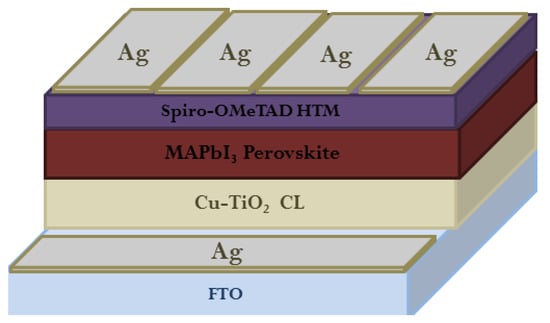
- Zaky, A.A.; Christopoulos, E.; Gkini, K.; Arfanis, M.K.; Sygellou, L.; Kaltzoglou, A.; Stergiou, A.; Tagmatarchis, N.; Balis, N.; Falaras, P. Enhancing efficiency and decreasing photocatalytic degradation of perovskite solar cells using a hydrophobic copper-modified titania electron transport layer. Appl. Catal. B Environ. 2021, 284, 119714.
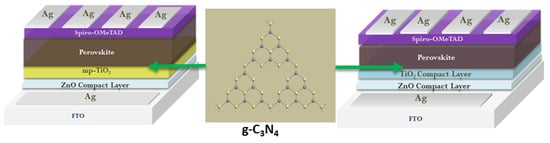
- Liu, Z.; Wu, S.; Yang, X.; Zhou, Y.; Jin, J.; Sun, J.; Zhao, L.; Wang, S. The dual interfacial modification of 2D g-C3N4 for high-efficiency and stable planar perovskite solar cells. Nanoscale Adv. 2020, 2, 5396–5402.
- Gkini, K.; Martinaiou, I.; Botzakaki, M.; Tsipas, P.; Theofylaktos, L.; Dimoulas, A.; Katsaros, F.; Stergiopoulos, T.; Krontiras, C.; Georga, S.; et al. Energy band tuning induced by g-C3N4 interface engineering for efficient and stable perovskite solar cells. Mater. Today Commun. 2022, 32, 103899.