Among all the lead-free perovskite materials, lead-free double perovskite has emerged as a very promising candidate to address both the stability and toxicity issues in lead-based perovskites. Theoretically, lead-free double perovskite can be designed and synthesized by replacing Pb
2+ with a low- or non-toxic metal ion. To maintain charge neutrality, two Pb
2+ cations can usually be replaced by one monovalent metal cation M(I) and a trivalent metal cation M(III) to form the double perovskite with a general formula of A
2M(I)M(III)X
6, where M(I) = Na
+, K
+, Rb
+, Cu
+, Ag
+, Au
+, In
+, and Tl
+, and M(III) = Bi
3+, Sb
3+, In
3+, Au
3+, Tl
3+, and Fe
3+. Two Pb
2+ ions can also be replaced by one tetravalent metal cation M(IV) to form the vacancy-ordered double perovskite with a general formula of A
2M(IV)X
6, where A = MA
+, FA
+, and Cs
+, M(IV) = Sn
4+, Ge
4+, Ti
4+, Pd
4+, Hf
4+, Te
4+, Zr
4+, and Cr
4+, and X = Cl
−, Br
−, and I
−. The A
2M(I)M(III)X
6 compounds are historically known as elpasolites after the mineral elpasolite, K
2NaAlF
6. The first reported synthesis of an elpasolite was Cs
2Au(I)Au(III)Cl
6 in 1922
[3]. Since the 1970s, researchers have been exploring the mixed valence state in elpasolites. In 2003, Guloy et al. successfully synthesized the first 2D perovskite A
2[(Au(I)I
2)(Au(III)I
4)(I
3)
2] (A = 1.8 octanodiammonium or 1,7-heptadione)
[4]. After extensive experiments, Hemamala et al. reported the synthesis of Cs
2AgBiBr
6 in 2016
[5]. Subsequently, various applications based on A
2M(I)M(III)X
6 perovskite have been widely developed. The origin of A
2M(IV)X
6 perovskite can be traced back to the synthesis of A
2TeX
6 (A = K
+, Na
+, and X = Cl
−, Br
−, I
−) in 1834
[6]. Before the 1920s, researchers mainly studied its synthesis, elemental analysis, and crystal morphology. In 2014, A
2M(IV)X
6-type perovskite was first applied in a photovoltaic device. Regarding the development of a double perovskite-based photodetector, in 2017, Tang et al. first reported the application of ultraviolet detection and X-ray detection using the lead-free double perovskites Cs
2AgInCl
6 and Cs
2AgBiBr
6, respectively. Since then, double perovskite photodetectors have made great progress. In addition to A
2M(IV)X
6, vacancy-ordered double perovskites, such as Cs
2SnI
6, Cs
2PdBr
6, etc., have also been successfully implemented for the fabrication of UV photodetectors.
2. Challenges and Perspective for Lead-Free Double Perovskite-Based PDs
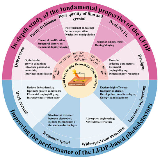
As mentioned in the previous section, lead-free double perovskite photodetectors have received a lot of research attention in recent years and have achieved impressive progress. Despite the tremendous progress in photodetection, there are still many challenges in the future direction of this field, which may hinder the development of lead-free double perovskite and limit its potential applications. Researchers systematically summarize the challenges faced by the use of various types of lead-free double perovskite to fabricate higher-performance photodetectors, and
reswe
archers propose the corresponding solutions, as summarized in
Figure 1 and discussed as follows:
Figure 1. Summary of the challenges and viable strategies of the lead-free double perovskite photodetectors.
(1) In-depth understanding of the fundamental material properties of the lead-free double perovskite is needed. Compared with the well-studied lead-based perovskite, lead-free double perovskite, as a new branch of perovskite materials, is undoubtedly underinvested and many aspects have not been effectively or deeply investigated. To explore the potential of lead-free double perovskite, researchers need to investigate more deeply its potential mechanism, crystal structure, and optoelectronic properties.
ResWe
archers summarize five material challenges that limit the wide application of double perovskite in optoelectronics. First, compared to the conventional lead-based perovskite, double perovskite has more deep-level defect states in the lattice and bulk phases, which reduces its carrier mobility and lifetime. To understand the mechanism of defect traps in the structure, the basic charge carrier dynamics need to be studied in detail. The growth condition needs to be carefully tuned to obtain high-quality perovskite absorbers. Meanwhile, the methods of the defect passivation and surface modification of lead-free perovskite should be explored. For example, the incorporation of non-volatile Lewis-base molecules such as urea and thiourea into the perovskite precursor solution can regulate crystal growth and cause single crystals to precipitate along grain boundaries to passivate defects
[7][86].
Second, for some lead-free double perovskites with indirect bandgaps, such as Bi-based, Sb-based, and Ti-based, they require phonon emission or absorption to maintain momentum, which lead to their relatively low absorption coefficients
[8][87]. Bandgap engineering can modulate the optoelectronic properties of lead-free double perovskite to make the transition from indirect bandgap to direct bandgap. The engineering strategy mainly consists of elemental doping/alloying and tuning the ordering parameters. Doping and alloying are the most powerful methods for adjusting the optical, electrical, and structural properties of perovskite
[9][88]. For example, through alloying with In
3+ or Sb
3+, the indirect bandgap of bulk Cs
2AgBiBr
6 (2.12 eV) has been altered to 2.27 and 1.86 eV, respectively, which is caused by the different atomic configurations of In and Sb. However, most of the In and Sb alloyed samples show reduced PL intensity, suggesting the presence of relatively deep defect states. The ordered-disorder parameters can be intentionally adjusted through growth regulation or external pressure treatment, resulting in changes in the bandgap
[9][88]. Direct bandgaps can be also achieved from some low-dimension structures such as the (BA)
4AgBiBr
8 [10][89] and (AE2T)
2AgBiI
8 [11][90]. In addition, doping VA group elements (Sb
3+, Bi
3+) in the Cs
2NaInCl
6 material can significantly improve the light absorption intensity of the material in the near-ultraviolet region, which can be applied to wide-spectrum photodetection.
[12][91]
Third, for double perovskite compounds with direct but parity-forbidden transition gaps, such as Cs
2AgInCl
6, Cs
2AgTlCl
6, Cs
2NaInCl
6, and Cs
2TiBr
6, they have poor absorption ability for photons with energies close to the bandgap. Chemical modification, structural distortion or elemental doping can be used to eliminate or break the optical transition selection rules and make them more suitable for photoelectrical applications. For example, alloying Na
+ into Cs
2AgInCl
6 can efficiently break the parity-forbidden transition of the host material
[13][92].
Fourth, the preparation of dense and uniform high-quality thin films is a major challenge for almost all lead-free double perovskite detectors. For Bi
3+-based, Sn
4+-based, In
3+-based, Au
3+-based, and Sb
3+-based double perovskite, their precursor materials are mostly insoluble in organic solvents, thus making it difficult to obtain pure-phase films when preparing films by the spin-coating method.
RWe
searchers sh should explore more effective synthesis strategies to prepare high-quality lead-free double perovskite with optimized morphologies. Among them, proper post-thermal annealing treatment of spin-coated films is an effective option. In addition, using vacuum thermal evaporation to prepare double perovskite thin films is also feasible. For example, the self-powered UV photodetector, which is based on Cs
2AgBiBr
6 thin film prepared by sequential vacuum evaporation method, has obtained a high on/off ratio of 6.6 × 10
3 and a fast response time of 6.13/28.02 μs
[14][85]. In addition, the synthesis of pure-phase and large-size single crystals is also crucial for the development of lead-free double perovskite detectors. Compared with thin films, bulk single crystals display the advantages of fewer defects and high stability. For Sb
3+-based double perovskite with a high formation energy, the synthesis of pure-phase single crystals remains to be explored. Accordingly,
rwe
searchers should deepen
theour understanding of the crystallization mechanism involved in the synthesis process, which can help to improve the morphology of the films and single crystals, thus optimizing the device performance.
Finally, for some double perovskites which have very weak or no PL emission, such as Fe
3+-based, Au
3+-based, and Ti
4+-based
[15][93] double perovskites,
rwe
searchers need to understand the possible reasons behind these properties such as the indirect bandgap, and the parity-forbidden direct/indirect transition, and then solve the problems using strategies such as doping, alloying, and tailoring the dimensionality. In the meanwhile, it is also essential to invest more efforts into the exploration of new materials with other structures. For example, the lead-free stable oxide double perovskite A
2M(III)M(V)O
6 (A = Ca, Sr, Ba; M(V) = V
5+, Nb
5+, or Ta
5+), which is transformed from prototype perovskite oxide CaTiO
3, has been used as an absorbing layer material for photodetectors. Among them, a self-powered ITO/BBNO/Ag photodetector based on Ba
2Bi
1.5Nb
0.5O
6 (Eg = 1.37 eV) has shown an optical response in the range of 365–760 nm and exhibited a photocurrent of 59.2 mA cm
−2 and a response of 78.8 mA W
−1 [16][94]. Another structurally similar calcium niobate Ca
2Nb
2.5Ta
0.5O
10 nanosheet is also used as the photoactive layer of the detector, and the device shows a switching ratio of 5.6 × 10
4 and a responsiveness of up to 469.5 A W
−1 at 1 V bias and 295 nm illumination
[17][95]. In addition to the above oxide perovskite, the A
3M(I)M(III)X
7 2D materials also deserve more in-depth study. Very recently, researchers have conducted a detailed study of Cs
3AgBiBr
7 based on the first principles. The results show that the material exhibits significant light absorption in the UV range, despite its low carrier mobility
[18][96]. Moreover, the photodetector based on (n-propylammonium)
2CsAgBiBr
7 single crystals exhibits a large on/off ratio (≈10
4) and a high detection rate (5.3 × 10
11 Jones) at 405 nm light
[19][97]. Their study provides a potential avenue for the design of various perovskite-based photodetectors.
(2) The device performance needs to be further improved. The ideal photodetector should have excellent spectral response range tunability, high responsivity, high sensitivity, low noise, and high stability. Looking into the future, research on how to improve the performance of lead-free double perovskite photodetectors can start from four aspects, including reducing dark current, increasing response speed, fabricating the wide-spectrum photodetector, and engineering the interface of the devices.
First, a lower dark current is a prerequisite for high detectivity. For semiconductor-based photodetectors, the dark current is closely related to the defect density of the materials. However, the crystal defects of lead-free double perovskite are much more numerous than those of lead-based perovskite. For example, the Bi
Ag and halogen vacancies in Bi
3+-based double perovskite and In
Ag in In
3+-based double perovskite are deep electron traps, and these unnecessary deep-level defects strongly affect the carrier density and transport. In the meanwhile, the direct contact between the perovskite layer and the functional layer can cause interface recombination loss, and the combined effects of these factors will lead to a higher dark current in the device. Optimizing the growth conditions or metal ion doping can suppress internal defects in the crystal, while introducing a passivation layer on the surface of perovskite can eliminate the surface defects. These strategies can effectively reduce the dark current of the device and improve the detectivity. For example, doping Rb
+ in the Cs
2AgBiBr
6 crystal can improve its response to X-rays due to the extended carrier lifetime, significant reduction of dark current, and polarization formation
[20][98].
Second, in optical communication and time-of-flight imaging applications, the high response speed of detectors is essential. In theory, reducing the time required for carrier diffusion and charge collection helps to obtain high-speed photodetectors. When designing lead-free double perovskite-based photodetectors, the strategy of shortening the distance between electrodes can improve charge collection efficiency. For detectors with vertical structures, reducing the thickness of the semiconductor layer can achieve a rapid response of the device.
Third, the research of wide-spectrum photodetectors based on lead free double perovskite will be an important research field for future photodetectors. The narrow bandgap characteristic of perovskite is the primary condition for achieving wide spectral detection. For Sb
3+-based, Ti
4+-based, Fe
3+-based, Au
3+-based, and Sn
4+-based double perovskite, their bandgaps are relatively small, making them suitable candidates for manufacturing wide spectral detectors. For Bi
3+-based, In
3+-based, and other large-bandgap double perovskite, energy band engineering is an effective way to adjust their bandgaps and design suitable carrier leap modes. Another commonly used strategy for achieving broadband detection (in the visible and near-infrared regions) is to integrate perovskite with low-bandgap polymers or organic small molecules, such as CyPF
6, Cy1BF
4 [21][99], NDI-DPP
[22][100], PTB7-Th
[23][101], and so on. For example, a broadband detector can be fabricated by combining perovskite with low-bandgap PDPPTDTPT, which shows a spectral response range of 350 nm to 1050 nm and an ultrafast response rate of 5 ns at a wavelength of 800 nm
[24][102].
Finally, to achieve high-performance photodetectors, interface engineering is needed to improve the charge separation and extraction rates
[25][103]. In optoelectronic devices, solution-based prepared perovskite films have many pinholes and surface defects, and the perovskite materials are usually sensitive to the surface conditions of adjacent layers, which requires the introduction of appropriate insertion layers to alleviate the impact of these unfavorable factors on device performance
[26][104]. Introducing functionalized interlayers can promote favorable interface charge dynamics and minimize the carrier loss of interfacial dipoles, ultimately improving device performance. For example, F4-TCNQ layer (2,3,5,6-tetrafluoro-7,7,8,8-tetracyanoquinodimethane) was introduced between NiO
x/perovskite layers, and it can increase the hole concentration and work function of NiO
x HTL and thus can improve hole extraction and carrier mobility
[27][105]. Functionalized interlayers, such as the ALD-MO
x interlayer mentioned before, can also significantly optimize the quality of perovskite films. In addition, a suitable interface layer facilitates the ideal energy band alignment between the perovskite and the transport layers. Currently, the ETLs used for perovskite photodetectors are usually metal oxides such as ZnO, TiO
2, and SnO
2. However, at the ETL and perovskite interface,
rwe
searchers usually observe non-radiative recombination and low electron extraction efficiency, so it is necessary to introduce an additional interface layer to alleviate these problems. For example, ZrCl
4 can modify the TiO
2 ETL by eliminating the offset between the conduction band edge of the TiO
2 transport layer and the absorber and improving the charge extraction efficiency; thus, perovskite solar cells based on modified ETL achieved a much higher stable efficiency
[28][106]. Regarding interface engineering, future research can focus on developing multifunctional molecular interface materials that can simultaneously passivate the defects, enhance the device carrier extraction, and extend the device lifetime
[29][107].
RWe
searchers believe that the performance of lead-free double perovskite-based photodetectors will improve gradually and move closer to commercialization as more and more researchers are involved.
Based on the above discussions, although the performance of lead-free double perovskite photodetectors may be inferior to that of lead halide devices, there is no doubt that lead-free double perovskite has unlimited potential for applications in optoelectronic devices such as photodetectors. With a deeper understanding of the fundamental physical and optical properties of lead-free double perovskite,
rwe
searchers can completely achieve photodetectors with stable performance, environmental friendliness, and high commercial value. The technology of lead-free perovskite photodetectors is young and promising, and we believe that its developmental path will become more and more open and bright.