Reducing the economic and environmental impact of industrial process may be achieved by the smartisation of different components. In this work, tube smartisation is presented via direct fabrication of a copper (Cu)-based resistive temperature detector (RTD) on their outer surfaces. The testing was carried out between room temperature and 250 °C. For this purpose, copper depositions were studied using mid-frequency (MF) and high-power impulse magnetron sputtering (HiPIMS). Stainless steel tubes with an outside inert ceramic coating were used after giving them a shot blasting treatment. The Cu deposition was performed at around 425 °C to improve adhesion as well as the electrical properties of the sensor. To generate the pattern of the Cu RTD, a photolithography process was carried out. The RTD was then protected from external degradation by a silicon oxide film deposited over it by means of two different techniques: sol–gel dipping technique and reactive magnetron sputtering.
1. Introduction
In an industry that is increasingly moving towards a digital form of business, the need to be connected to its production processes is increasing. In the Industry 4.0 era, the acquisition of the information regarding the status of these processes is highly valued. In sectors as diverse as chemical, power generation, or food, the critical parameters of both the process and the equipment must be monitored during a large part of the production process
[1][2][3][4][5][6][1,2,3,4,5,6]. For a long time, the interest of companies in these and other sectors has focused on knowing the state of the fluids that circulate inside the pipes throughout their plants and equipment. Continuous monitoring prevents critical system failures, avoids leaks and energy losses, and thus helps keep costs down
[7][8][9][10][7,8,9,10]. Meanwhile, the interest of the companies supplying this equipment has been to offer this service, justified by the interest it arouses.
However, most of the monitoring methods on the market are limited by their size or their high degree of invasion in critical processes. For this reason, in recent years, sensorisation and monitoring have evolved towards less invasive and more embedded methods
[11][12][13][11,12,13]. Their benefits include maintaining the integrity of the pipes, thus ensuring greater safety, and ultimately lower installation and maintenance costs
[14][15][14,15]. Among the existing methods (ultrasound, Eddy current, thermography, etc.) thin-layer sensors have the advantage of being able to be installed in areas which are difficult to access, in addition to presenting a faster response to changes in the system
[16][17][18][16,17,18].
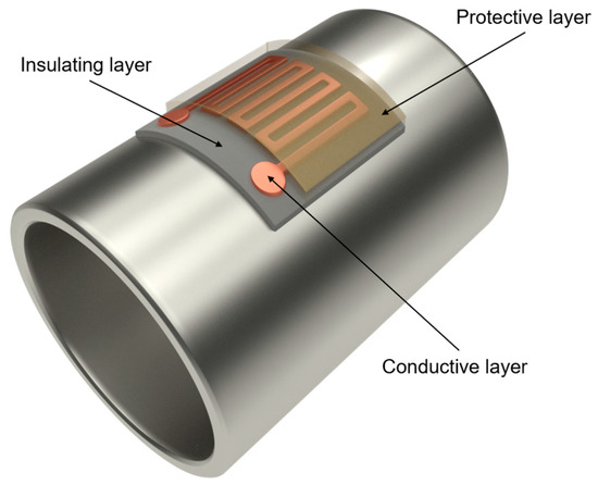
As is known from the literature, a resistive temperature detector (RTD) is a device that changes its electrical resistance value according to the temperature, and it can be mainly classified in three categories: wire-wound, coiled elements, and thin-film. These sensors usually present better accuracy compared with other temperature sensors such as thermocouples. In the case of a sensor based on a thin-film RTD, this can be composed of various thin layers. A typical example of a multilayer sensor for a tube may have the following configuration (Figure 1):
Figure 1. Layout of the temperature sensor.
-
A layer of electrical insulator on the surface of the stainless-steel tube. Its function is to avoid electrical contact between the sensor layer and the tube.
-
An electrically conductive or sensing layer, which is the RTD itself. This metallic layer has a varied electrical resistance as the temperature changes.
-
A protective layer to protect the sensor layer from degradation phenomena such as high-temperature oxidation.
Therefore, in the context of this work, the RTD designation will refer to the sensor layer; that is, the copper layer. Meanwhile, the device made up of multiple layers will be defined as the temperature sensor.
Concerning the sensing layer, platinum is commonly used as a sensing material due to its excellent corrosion resistance and electrical response with good linearity for wide ranges of temperature
[19][20][21][22][23][19,20,21,22,23], but its use implies a high economic impact in its industrial production. As a cheaper alternative, other materials have been studied, such as nickel
[24][25][26][27][24,25,26,27] or aluminium
[28][29][28,29]. In some of these studies, transfer processes of the pattern to a curved substrate have been carried out, requiring complex methods and several materials.
In the current contribution, a copper RTD for ceramic-coated stainless-steel tubes is introduced. In the past, few works reporting Cu-based
[30][31][30,31] and combined Ti–Cu
[32] and Cu–Ni
[33] systems have been published, although the temperature range covered in those works is significantly lower. Details on the fabrication of a copper layer and a simple method patterning are provided, as well as the results of electrical tests carried out on a home-made prototype.
2. Design of the Sensor Layer
An RTD needs an electrical circuit through which electrons circulate, usually made of a metal that will see its electrical resistance changed with the variation in temperature. By measuring this electrical resistance change, it is possible to measure the variation in temperature. In the case of metals, the electrical resistance increases with increasing temperature
[34].
The model that currently best explains the behaviour of metals in solid structures is the band theory, being based on molecular orbitals and approximating the quantum state of a solid. Having a high number of valence orbitals, the energy levels together are considered to form continuous bands. Thus, two types of bands are differentiated: valence bands, where all the valence electrons of the atoms are found; and the conduction bands, where free electrons are found and responsible for conducting the electric current. In the case of a conductive material, these two bands will overlap or the gap between them will be minimal, allowing the electrons to jump between the bands. As the temperature of the metallic solid increases, the number of phonons generated within the material increases and they collide with the electrons, causing them to scatter. At the macroscopic level, this leads to an increase in the electrical resistivity of the material.
It is known that the resistance at room temperature (20–25 °C) of a circuit depends on its resistivity at that temperature (ρ), and the geometric parameters of the circuit (l: length, A: cross-section), for a uniform material and a constant cross-section:
For a wide temperature range, the following linear relationship between resistance and temperature holds, where
α is the temperature coefficient of resistance: