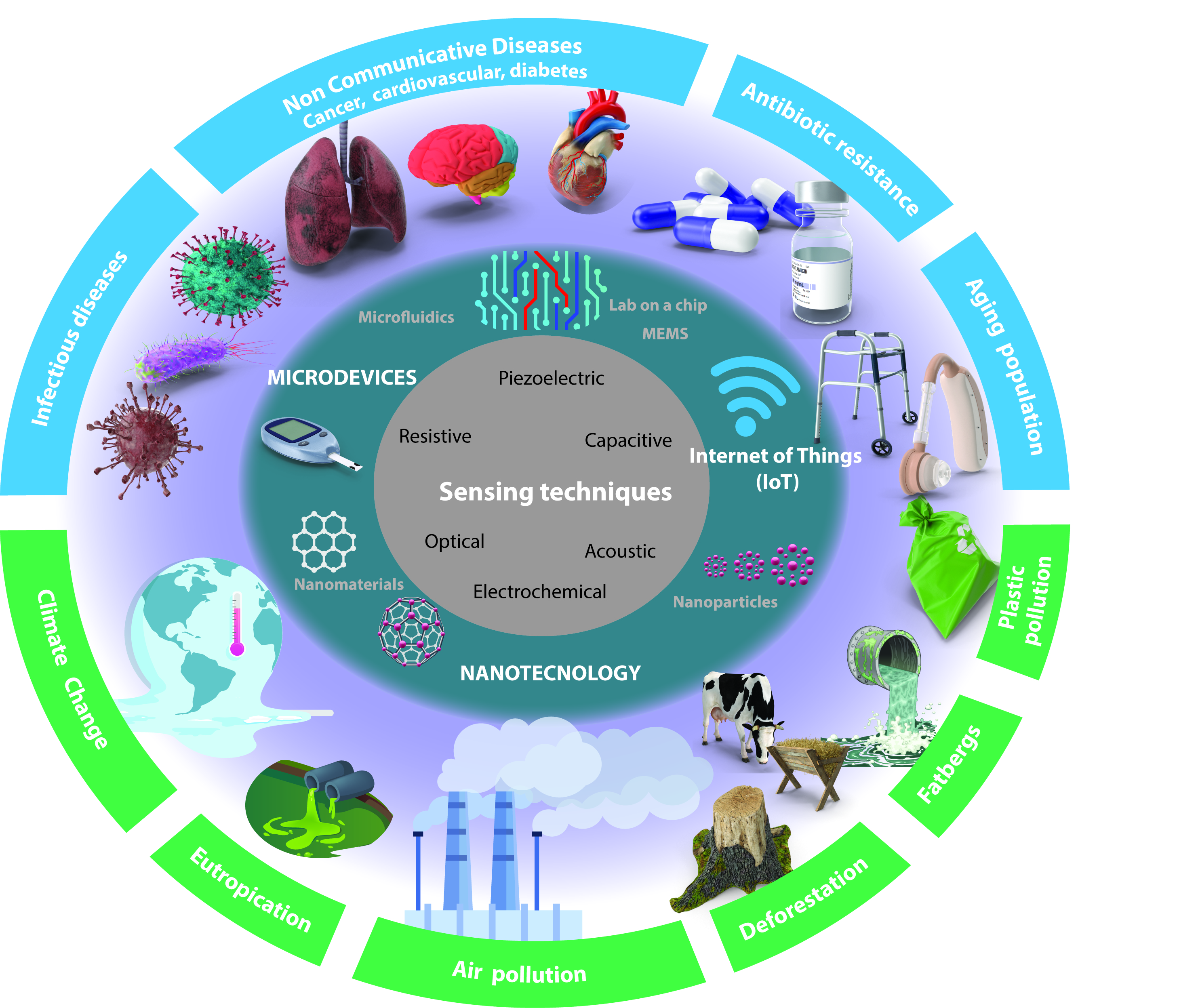
Micro- and nanotechnology-enabled sensors have made remarkable advancements in the fields of biomedicine and the environment, enabling the sensitive and selective detection and quantification of diverse analytes. In biomedicine, these sensors have facilitated disease diagnosis, drug discovery, and point-of-care devices. In environmental monitoring, they have played a crucial role in assessing air, water, and soil quality, as well as ensured food safety. Despite notable progress, numerous challenges persist. This review article addresses recent developments in micro- and nanotechnology-enabled sensors for biomedical and environmental challenges, focusing on enhancing basic sensing techniques through micro/nanotechnology. Additionally, it explores the applications of these sensors in addressing current challenges in both biomedical and environmental domains. The article concludes by emphasizing the need for further research to expand the detection capabilities of sensors/devices, enhance sensitivity and selectivity, integrate wireless communication and energy-harvesting technologies, and optimize sample preparation, material selection, and automated components for sensor design, fabrication, and characterization.
- microtechnology
- nanotechnology
- sensors
- biomedical
- enviromental
- non communicative
- diabetes
- cardiovascular
- cancer
- mental health
- plastic pollution
- eutrophication
- deforestation
- air pollution
- climate change
- fatberg
1. Introduction
2. Innovations Enabled by Nanotechnology in Sensing Techniques
2.1. Resistive Sensing
2.2. Capacitive Sensing
2.3. Piezoelectricity Sensing

2.4. Thermoelectricity Sensing
2.5. Acoustic Sensing
2.6. Electrochemical Sensing
2.7. Optical Sensing
2.7.1. Photodetection Sensing
2.7.2. Plasmonic Nanosensors

2.7.3. Photonic Crystals
References
- Rasmi, Y.; Saloua, K.S.; Nemati, M.; Choi, J.R. Recent Progress in Nanotechnology for COVID-19 Prevention, Diagnostics and Treatment. Nanomaterials 2021, 11, 1788.
- Pal, M.; Khan, R. Biosensor platforms for detection of cardiovascular disease risk biomarkers. In Functional Polysaccharides for Biomedical Applications; Elsevier: Amsterdam, The Netherlands, 2019; pp. 397–431.
- Kristoffersson, A.; Lindén, M. Wearable Sensors for Monitoring and Preventing Noncommunicable Diseases: A Systematic Review. Information 2020, 11, 521.
- Ndebele, R.T.; Yao, Q.; Shi, Y.N.; Zhai, Y.Y.; Xu, H.L.; Lu, C.T.; Zhao, Y.Z. Progress in the Application of Nano- and Micro-based Drug Delivery Systems in Pulmonary Drug Delivery. BIO Integr. 2022, 3, 71–83.
- Wan, H.; Zhuang, L.; Pan, Y.; Gao, F.; Tu, J.; Zhang, B.; Wang, P. Biomedical sensors. In Biomedical Information Technology; Elsevier: Amsterdam, The Netherlands, 2020; pp. 51–79.
- Botturi, A.; Ozbayram, E.G.; Tondera, K.; Gilbert, N.I.; Rouault, P.; Caradot, N.; Gutierrez, O.; Daneshgar, S.; Frison, N.; Akyol, C.; et al. Combined sewer overflows: A critical review on best practice and innovative solutions to mitigate impacts on environment and human health. Crit. Rev. Environ. Sci. Technol. 2021, 51, 1585–1618.
- Zhang, P.; Guo, Z.; Ullah, S.; Melagraki, G.; Afantitis, A.; Lynch, I. Nanotechnology and artificial intelligence to enable sustainable and precision agriculture. Nat. Plants 2021, 7, 864–876.
- Orlando, M.; Molla, G.; Castellani, P.; Pirillo, V.; Torretta, V.; Ferronato, N. Microbial Enzyme Biotechnology to Reach Plastic Waste Circularity: Current Status, Problems and Perspectives. Int. J. Mol. Sci. 2023, 24, 3877.
- Hasan, M.N.; Nafea, M.; Nayan, N.; Mohamed Ali, M.S. Thermoelectric Generator: Materials and Applications in Wearable Health Monitoring Sensors and Internet of Things Devices. Adv. Mater. Technol. 2022, 7, 2101203.
- Iyer, S.; Zhao, L.; Mohan, M.P.; Jimeno, J.; Siyal, M.Y.; Alphones, A.; Karim, M.F. mm-Wave Radar-Based Vital Signs Monitoring and Arrhythmia Detection Using Machine Learning. Sensors 2022, 22, 3106.
- Moabelo, K.L.; Martin, D.R.; Fadaka, A.O.; Sibuyi, N.R.S.; Meyer, M.; Madiehe, A.M. Nanotechnology-Based Strategies for Effective and Rapid Detection of SARS-CoV-2. Materials 2021, 14, 7851.
- Santos, B.S.; Cunha, J.L.; Carvalho, I.C.; Costa, J.M.; Longo, B.C.; Galinari, G.C.; Diniz, P.H.; Mendes, G.M.; Fonseca, F.G.; Abrahão, J.S.; et al. Nanotechnology meets immunology towards a rapid diagnosis solution: The COVID-19 outbreak challenge. RSC Adv. 2022, 12, 31711–31728.
- Campos, E.V.R.; de Oliveira, J.L.; Abrantes, D.C.; Rogério, C.B.; Bueno, C.; Miranda, V.R.; Monteiro, R.A.; Fraceto, L.F. Recent Developments in Nanotechnology for Detection and Control of Aedes aegypti-Borne Diseases. Front. Bioeng. Biotechnol. 2020, 8, e00102.
- Marzocchi, U.; Revsbech, N.P. Sulfate biosensor for environmental applications. Limnol. Oceanogr. Methods 2022, 20, 674–681.
- Peydayesh, M. Nanofiltration Membranes: Recent Advances and Environmental Applications. Membranes 2022, 12, 518.
- Saleem, H.; Zaidi, S.J.; Ismail, A.F.; Goh, P.S. Advances of nanomaterials for air pollution remediation and their impacts on the environment. Chemosphere 2022, 287, 132083.
- Sharma, C.; Dhiman, R.; Rokana, N.; Panwar, H. Nanotechnology: An Untapped Resource for Food Packaging. Front. Microbiol. 2017, 8, e01735.
- Kulkarni, M.B.; Ayachit, N.H.; Aminabhavi, T.M. Recent Advances in Microfluidics-Based Electrochemical Sensors for Foodborne Pathogen Detection. Biosensors 2023, 13, 246.
- Hua, Z.; Yu, T.; Liu, D.; Xianyu, Y. Recent advances in gold nanoparticles-based biosensors for food safety detection. Biosens. Bioelectron. 2021, 179, 113076.
- Ziani, K.; Ioniță-Mîndrican, C.B.; Mititelu, M.; Neacșu, S.M.; Negrei, C.; Moroșan, E.; Drăgănescu, D.; Preda, O.T. Microplastics: A Real Global Threat for Environment and Food Safety: A State of the Art Review. Nutrients 2023, 15, 617.
- Choi, G.; Murphy, E.; Guan, W. Microfluidic Time-Division Multiplexing Accessing Resistive Pulse Sensor for Particle Analysis. ACS Sens. 2019, 4, 1957–1963.
- Pollard, M.; Maugi, R.; Platt, M. Multi-resistive pulse sensor microfluidic device. Analyst 2022, 147, 1417–1424.
- Suhito, I.R.; Koo, K.M.; Kim, T.H. Recent Advances in Electrochemical Sensors for the Detection of Biomolecules and Whole Cells. Biomedicines 2020, 9, 15.
- Daniel, M.; Mathew, G.; Anpo, M.; Neppolian, B. MOF based electrochemical sensors for the detection of physiologically relevant biomolecules: An overview. Coord. Chem. Rev. 2022, 468, 214627.
- Nocerino, V.; Miranda, B.; Tramontano, C.; Chianese, G.; Dardano, P.; Rea, I.; De Stefano, L. Plasmonic Nanosensors: Design, Fabrication, and Applications in Biomedicine. Chemosensors 2022, 10, 150.
- Mondal, B.; Zeng, S. Recent Advances in Surface Plasmon Resonance for Biosensing Applications and Future Prospects. In Nanophotonics in Biomedical Engineering; Springer: Singapore, 2021; pp. 21–48.
- Lin, B.; Liu, H.; Huang, C.; Xiao, X.; Pedersen-Bjergaard, S.; Shen, X. Versatile Integration of Liquid-Phase Microextraction and Fluorescent Aptamer Beacons: A Synergistic Effect for Bioanalysis. Anal. Chem. 2021, 93, 14323–14333.
- Moutsiopoulou, A.; Broyles, D.; Dikici, E.; Daunert, S.; Deo, S.K. Molecular Aptamer Beacons and Their Applications in Sensing, Imaging, and Diagnostics. Small 2019, 15, 1902248.
- Zheng, W.W.; Yang, L.T.; Zhou, H.; Zhang, Z.Y.; Wang, X.Y.; Wu, J.Y.; Lu, X.C.; Chen, J.; Duan, C.W.; Chen, K.M. A novel aptamer beacon for rapid screening of recombinant cells and in vivo monitoring of recombinant proteins. Appl. Microbiol. Biotechnol. 2023, 107, 553–567.
- Zhao, L.; Wang, Q.; Yin, Y.; Yang, Y.; Cui, H.; Dong, Y. Evolution of Interferon-Gamma Aptamer with Good Affinity and Analytical Utility by a Rational In Silico Base Mutagenesis Post-SELEX Strategy. Molecules 2022, 27, 5725.
- Sun, Y.; Jiang, Q.; Chen, F.; Cao, Y. Paper-based electrochemical sensor. Electrochem. Sci. Adv. 2022, 2, e2100057.
- Smith, S.; Madzivhandila, P.; Ntuli, L.; Bezuidenhout, P.; Zheng, H.; Land, K. Printed Paper—Based Electrochemical Sensors for Low-Cost Point-of-Need Applications. Electrocatalysis 2019, 10, 342–351.
- Hou, Y.; Lv, C.C.; Guo, Y.L.; Ma, X.H.; Liu, W.; Jin, Y.; Li, B.X.; Yang, M.; Yao, S.Y. Recent Advances and Applications in Paper-Based Devices for Point-of-Care Testing. J. Anal. Test. 2022, 6, 247–273.
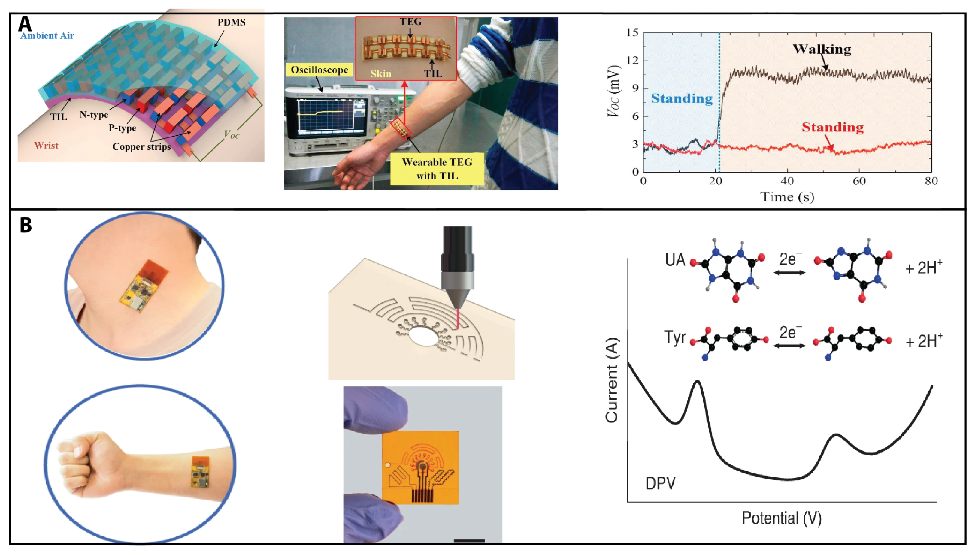
- Yang, Y.; Song, Y.; Bo, X.; Min, J.; Pak, O.S.; Zhu, L.; Wang, M.; Tu, J.; Kogan, A.; Zhang, H.; et al. A laser-engraved wearable sensor for sensitive detection of uric acid and tyrosine in sweat. Nat. Biotechnol. 2020, 38, 217–224.
- Singh, S.; Gill, A.A.S.; Nlooto, M.; Karpoormath, R. Prostate cancer biomarkers detection using nanoparticles based electrochemical biosensors. Biosens. Bioelectron. 2019, 137, 213–221.
- Kaushik, A.M.; Hsieh, K.; Mach, K.E.; Lewis, S.; Puleo, C.M.; Carroll, K.C.; Liao, J.C.; Wang, T. Droplet-Based Single-Cell Measurements of 16S rRNA Enable Integrated Bacteria Identification and Pheno-Molecular Antimicrobial Susceptibility Testing from Clinical Samples in 30 min. Adv. Sci. 2021, 8, 2003419.
- Singh, S.; Numan, A.; Cinti, S. Point-of-Care for Evaluating Antimicrobial Resistance through the Adoption of Functional Materials. Anal. Chem. 2022, 94, 26–40.
- Vasala, A.; Hytönen, V.P.; Laitinen, O.H. Modern Tools for Rapid Diagnostics of Antimicrobial Resistance. Front. Cell. Infect. Microbiol. 2020, 10, e00308.
- Cañadas-Ortega, M.; Gómez-Cruz, C.; Vaquero, J.J.; Muñoz-Barrutia, A. The contribution of microfluidics to the fight against tuberculosis. Nanotechnol. Rev. 2021, 11, 40–54.
- Postek, W.; Pacocha, N.; Garstecki, P. Microfluidics for antibiotic susceptibility testing. Lab A Chip 2022, 22, 3637–3662.
- Parsley, N.C.; Smythers, A.L.; Hicks, L.M. Implementation of Microfluidics for Antimicrobial Susceptibility Assays: Issues and Optimization Requirements. Front. Cell. Infect. Microbiol. 2020, 10, e547177.
- Moheimani, R.; Gonzalez, M.; Dalir, H. An Integrated Nanocomposite Proximity Sensor: Machine Learning-Based Optimization, Simulation, and Experiment. Nanomaterials 2022, 12, 1269.
- Arroyo, P.; Gómez-Suárez, J.; Suárez, J.I.; Lozano, J. Low-Cost Air Quality Measurement System Based on Electrochemical and PM Sensors with Cloud Connection. Sensors 2021, 21, 6228.
- Liu, Y.; Yao, L.; He, L.; Liu, N.; Piao, Y. Electrochemical enzyme biosensor bearing biochar nanoparticle as signal enhancer for bisphenol a detection in water. Sensors 2019, 19, 1619.
- de Almeida, D.S.; Martins, L.D.; Aguiar, M.L. Air pollution control for indoor environments using nanofiber filters: A brief review and post-pandemic perspectives. Chem. Eng. J. Adv. 2022, 11, 100330.
- Wang, H.; Yin, F.; Li, Z.; Su, W.; Li, D. Advances of microfluidic lung chips for assessing atmospheric pollutants exposure. Environ. Int. 2023, 172, 107801.
- Elli, G.; Hamed, S.; Petrelli, M.; Ibba, P.; Ciocca, M.; Lugli, P.; Petti, L. Field-Effect Transistor-Based Biosensors for Environmental and Agricultural Monitoring. Sensors 2022, 22, 4178.
- Samreen, T.; Rasool, S.; Kanwal, S.; Riaz, S.; Sidra-Tul-Muntaha; Nazir, M.Z. Role of Nanotechnology in Precision Agriculture. In Proceedings of the The 1st International Precision Agriculture Pakistan Conference 2022 (PAPC 2022)—Change the Culture of Agriculture, Rawalpindi, Pakistan, 22–24 September 2022; MDPI: Basel, Switzerland, 2022; p. 17.
- Faraji Rad, Z. Microneedle Technologies for Food and Crop Health: Recent Advances and Future Perspectives. Adv. Eng. Mater. 2023, 25, 2201194.
- Nakamura, H. Developmental Studies on Practical Enzymatic Phosphate Ion Biosensors and Microbial BOD Biosensors, and New Insights into the Future Perspectives of These Biosensor Fields; Intechopen: London, UK, 2022.
- Bhattacharyya, P.; Acharyya, D.; Dutta, K. Resistive and Capacitive Measurement of Nano-Structured Gas Sensors; Springer Nature: Cham, Switzerland, 2019; pp. 25–62.
- Feng, P.; Yuan, Y.; Zhong, M.; Shao, J.; Liu, X.; Xu, J.; Zhang, J.; Li, K.; Zhao, W. Integrated Resistive-Capacitive Strain Sensors Based on Polymer—Nanoparticle Composites. ACS Appl. Nano Mater. 2020, 3, 4357–4366.
- Han, Z.; Liu, J.; Liu, Z.; Pan, W.; Yang, Y.; Chen, X.; Gao, Y.; Duan, X. Resistive pulse sensing device with embedded nanochannel (nanochannel-RPS) for label-free biomolecule and bionanoparticle analysis. Nanotechnology 2021, 32, 295507.
- Sharma, R.K.; Agrawal, I.; Dai, L.; Doyle, P.; Garaj, S. DNA Knot Malleability in Single-Digit Nanopores. Nano Lett. 2021, 21, 3772–3779.
- Pollard, M.; Hunsicker, E.; Platt, M. A Tunable Three-Dimensional Printed Microfluidic Resistive Pulse Sensor for the Characterization of Algae and Microplastics. ACS Sens. 2020, 5, 2578–2586.
- Chaloeipote, G.; Samarnwong, J.; Traiwatcharanon, P.; Kerdcharoen, T.; Wongchoosuk, C. High-performance resistive humidity sensor based on Ag nanoparticles decorated with graphene quantum dots. R. Soc. Open Sci. 2021, 8, 210407.
- Duan, Y.; He, S.; Wu, J.; Su, B.; Wang, Y. Recent Progress in Flexible Pressure Sensor Arrays. Nanomaterials 2022, 12, 2495.
- Ma, Z.; Zhang, Y.; Zhang, K.; Deng, H.; Fu, Q. Recent progress in flexible capacitive sensors: Structures and properties. Nano Mater. Sci. 2022, in press.
- Mishra, R.B.; El-Atab, N.; Hussain, A.M.; Hussain, M.M. Recent Progress on Flexible Capacitive Pressure Sensors: From Design and Materials to Applications. Adv. Mater. Technol. 2021, 6, 2001023.
- Kim, Y.; Oh, J.H. Recent Progress in Pressure Sensors for Wearable Electronics: From Design to Applications. Appl. Sci. 2020, 10, 6403.
- Cao, J.; Zhang, X. Modulating the percolation network of polymer nanocomposites for flexible sensors. J. Appl. Phys. 2020, 128, 220901.
- Pohanka, M. The Piezoelectric Biosensors: Principles and Applications, a Review. Int. J. Electrochem. Sci. 2017, 12, 496–506.
- Fu, Y.; Luo, J.; Nguyen, N.; Walton, A.; Flewitt, A.; Zu, X.; Li, Y.; McHale, G.; Matthews, A.; Iborra, E.; et al. Advances in piezoelectric thin films for acoustic biosensors, acoustofluidics and lab-on-chip applications. Prog. Mater. Sci. 2017, 89, 31–91.
- Pan, C.; Zhai, J.; Wang, Z.L. Piezotronics and Piezo-phototronics of Third Generation Semiconductor Nanowires. Chem. Rev. 2019, 119, 9303–9359.
- Du, Y.; Du, W.; Lin, D.; Ai, M.; Li, S.; Zhang, L. Recent Progress on Hydrogel-Based Piezoelectric Devices for Biomedical Applications. Micromachines 2023, 14, 167.
- Hu, Z.; Li, J.; Wei, X.; Wang, C.; Cao, Y.; Gao, Z.; Han, J.; Li, Y. Enhancing Strain-Sensing Properties of the Conductive Hydrogel by Introducing PVDF-TrFE. ACS Appl. Mater. Interfaces 2022, 14, 45853–45868.
- Choi, J.; Kwon, D.; Kim, K.; Park, J.; Orbe, D.D.; Gu, J.; Ahn, J.; Cho, I.; Jeong, Y.; Oh, Y.; et al. Synergetic Effect of Porous Elastomer and Percolation of Carbon Nanotube Filler toward High Performance Capacitive Pressure Sensors. ACS Appl. Mater. Interfaces 2020, 12, 1698–1706.
- Peng, S.; Wang, D.; Lu, J.; He, M.; Xu, C.; Li, Y.; Zhu, S. A Review on Organic Polymer-Based Thermoelectric Materials. J. Polym. Environ. 2017, 25, 1208–1218.
- Sattar, M.; Yeo, W.H. Recent Advances in Materials for Wearable Thermoelectric Generators and Biosensing Devices. Materials 2022, 15, 4315.
- Gutiérrez Moreno, J.J.; Cao, J.; Fronzi, M.; Assadi, M.H.N. A review of recent progress in thermoelectric materials through computational methods. Mater. Renew. Sustain. Energy 2020, 9, 16.
- Jia, P.Z.; Xie, J.P.; Chen, X.K.; Zhang, Y.; Yu, X.; Zeng, Y.J.; Xie, Z.X.; Deng, Y.X.; Zhou, W.X. Recent progress of two-dimensional heterostructures for thermoelectric applications. J. Phys. Condens. Matter 2023, 35, 073001.
- Yang, S.; Qiu, P.; Chen, L.; Shi, X. Recent Developments in Flexible Thermoelectric Devices. Small Sci. 2021, 1, 2100005.
- Massetti, M.; Jiao, F.; Ferguson, A.J.; Zhao, D.; Wijeratne, K.; Würger, A.; Blackburn, J.L.; Crispin, X.; Fabiano, S. Unconventional Thermoelectric Materials for Energy Harvesting and Sensing Applications. Chem. Rev. 2021, 121, 12465–12547.
- Wang, Y.; Shi, Y.; Mei, D.; Chen, Z. Wearable thermoelectric generator for harvesting heat on the curved human wrist. Appl. Energy 2017, 205, 710–719.
- Ding, H.; Shu, X.; Jin, Y.; Fan, T.; Zhang, H. Recent advances in nanomaterial-enabled acoustic devices for audible sound generation and detection. Nanoscale 2019, 11, 5839–5860.
- Wei, L.; Kuai, X.; Bao, Y.; Wei, J.; Yang, L.; Song, P.; Zhang, M.; Yang, F.; Wang, X. The Recent Progress of MEMS/NEMS Resonators. Micromachines 2021, 12, 724.
- Kähler, H.; Platz, D.; Schmid, S. Surface acoustic wave coupling between micromechanical resonators. Commun. Phys. 2022, 5, 118.
- Gong, S.; Yap, L.W.; Zhu, Y.; Zhu, B.; Wang, Y.; Ling, Y.; Zhao, Y.; An, T.; Lu, Y.; Cheng, W. A Soft Resistive Acoustic Sensor Based on Suspended Standing Nanowire Membranes with Point Crack Design. Adv. Funct. Mater. 2020, 30, 1910717.
- Zhang, Q.; Ji, C.; Lv, L.; Zhao, D.; Ji, J.; Zhuo, K.; Yuan, Z.; Zhang, W.; Sang, S. A Flexible, Acoustic Localized Sensor with Mass Block–Beam Structure Based on Polydimethylsiloxane—Silver Nanowires. Soft Robot. 2021, 8, 352–363.
- Tonezzer, M. Detection of Mackerel Fish Spoilage with a Gas Sensor Based on One Single SnO2 Nanowire. Chemosensors 2020, 9, 2.
- Sartori, A.F.; Belardinelli, P.; Dolleman, R.J.; Steeneken, P.G.; Ghatkesar, M.K.; Buijnsters, J.G. Inkjet-Printed High-Q Nanocrystalline Diamond Resonators. Small 2019, 15, 1803774.
- Baranwal, J.; Barse, B.; Gatto, G.; Broncova, G.; Kumar, A. Electrochemical Sensors and Their Applications: A Review. Chemosensors 2022, 10, 363.
- Jin, Z.; Liu, Y.; Fan, W.; Huang, W. Integrating Flexible Electrochemical Sensor into Microfluidic Chip for Simulating and Monitoring Vascular Mechanotransduction. Small 2020, 16, 1903204.
- Meskher, H.; Mustansar, H.C.; Thakur, A.K.; Sathyamurthy, R.; Lynch, I.; Singh, P.; Han, T.K.; Saidur, R. Recent trends in carbon nanotube (CNT)-based biosensors for the fast and sensitive detection of human viruses: A critical review. Nanoscale Adv. 2023, 5, 992–1010.
- Shoaib, A.; Darraj, A.; Khan, M.E.; Azmi, L.; Alalwan, A.; Alamri, O.; Tabish, M.; Khan, A.U. A Nanotechnology-Based Approach to Biosensor Application in Current Diabetes Management Practices. Nanomaterials 2023, 13, 867.
- de Campos, A.M.; Silva, R.R.; Calegaro, M.L.; Raymundo-Pereira, P.A. Design and Fabrication of Flexible Copper Sensor Decorated with Bismuth Micro/Nanodentrites to Detect Lead and Cadmium in Noninvasive Samples of Sweat. Chemosensors 2022, 10, 446.
- Ghaffari, R.; Rogers, J.A.; Ray, T.R. Recent progress, challenges, and opportunities for wearable biochemical sensors for sweat analysis. Sens. Actuator Chem. 2021, 332, 129447.
- Gao, F.; Liu, C.; Zhang, L.; Liu, T.; Wang, Z.; Song, Z.; Cai, H.; Fang, Z.; Chen, J.; Wang, J.; et al. Wearable and flexible electrochemical sensors for sweat analysis: A review. Microsyst. Nanoeng. 2023, 9, 1.
- Li, Z.; Liu, C.; Sarpong, V.; Gu, Z. Multisegment nanowire/nanoparticle hybrid arrays as electrochemical biosensors for simultaneous detection of antibiotics. Biosens. Bioelectron. 2019, 126, 632–639.
- Zumpano, R.; Polli, F.; D’Agostino, C.; Antiochia, R.; Favero, G.; Mazzei, F. Nanostructure-Based Electrochemical Immunosensors as Diagnostic Tools. Electrochem 2021, 2, 10–28.
- Bertel, L.; Miranda, D.A.; García-Martín, J.M. Nanostructured Titanium Dioxide Surfaces for Electrochemical Biosensing. Sensors 2021, 21, 6167.
- Sinha, A.; Dhanjai; Tan, B.; Huang, Y.; Zhao, H.; Dang, X.; Chen, J.; Jain, R. MoS2 nanostructures for electrochemical sensing of multidisciplinary targets: A review. TrAC Trends Anal. Chem. 2018, 102, 75–90.
- Sabaté del Río, J.; Henry, O.Y.F.; Jolly, P.; Ingber, D.E. An antifouling coating that enables affinity-based electrochemical biosensing in complex biological fluids. Nat. Nanotechnol. 2019, 14, 1143–1149.
- Hui, R. Photodetectors. In Introduction to Fiber-Optic Communications; Elsevier: Amsterdam, The Netherlands, 2020; pp. 125–154.
- Li, Z.; Xu, K.; Wei, F. Recent progress in photodetectors based on low-dimensional nanomaterials. Nanotechnol. Rev. 2018, 7, 393–411.
- Yadav, P.K.; Ajitha, B.; Kumar Reddy, Y.A.; Sreedhar, A. Recent advances in development of nanostructured photodetectors from ultraviolet to infrared region: A review. Chemosphere 2021, 279, 130473.
- Ghosh, J.; Sellin, P.J.; Giri, P.K. Recent advances in lead-free double perovskites for X-ray and photodetection. Nanotechnology 2022, 33, 312001.
- Li, C.; Li, J.; Li, Z.; Zhang, H.; Dang, Y.; Kong, F. High-Performance Photodetectors Based on Nanostructured Perovskites. Nanomaterials 2021, 11, 1038.
- Tian, W.; Sun, H.; Chen, L.; Wangyang, P.; Chen, X.; Xiong, J.; Li, L. Low-dimensional nanomaterial/Si heterostructure-based photodetectors. InfoMat 2019, 1, 140–163.
- Yoo, T.J.; Kim, W.S.; Chang, K.E.; Kim, C.; Kwon, M.G.; Jo, J.Y.; Lee, B.H. High Gain and Broadband Absorption Graphene Photodetector Decorated with Bi2Te3 Nanowires. Nanomaterials 2021, 11, 755.
- Soler, M.; Huertas, C.S.; Lechuga, L.M. Label-free plasmonic biosensors for point-of-care diagnostics: A review. Expert Rev. Mol. Diagn. 2019, 19, 71–81.
- Huertas, C.S.; Bonnal, S.; Soler, M.; Escuela, A.M.; Valcárcel, J.; Lechuga, L.M. Site-Specific mRNA Cleavage for Selective and Quantitative Profiling of Alternative Splicing with Label-Free Optical Biosensors. Anal. Chem. 2019, 91, 15138–15146.
- Schasfoort, R.B.M. Introduction to Surface Plasmon Resonance. In Handbook of Surface Plasmon Resonance; The Royal Society of Chemistry: London, UK, 2017; pp. 1–26.
- Soler, M.; Lechuga, L.M. Principles, technologies, and applications of plasmonic biosensors. J. Appl. Phys. 2021, 129, 111102.
- Park, J.H.; Cho, Y.W.; Kim, T.H. Recent Advances in Surface Plasmon Resonance Sensors for Sensitive Optical Detection of Pathogens. Biosensors 2022, 12, 180.
- Huo, Z.; Li, Y.; Chen, B.; Zhang, W.; Yang, X.; Yang, X. Recent advances in surface plasmon resonance imaging and biological applications. Talanta 2023, 255, 124213.
- Knoerzer, M.; Szydzik, C.; Ren, G.; Huertas, C.S.; Palmer, S.; Tang, P.; Nguyen, T.G.; Bui, L.; Boes, A.; Mitchell, A. Optical frequency comb based system for photonic refractive index sensor interrogation. Opt. Express 2019, 27, 21532.
- Zhang, B.Y.; Yin, P.; Hu, Y.; Szydzik, C.; Khan, M.W.; Xu, K.; Thurgood, P.; Mahmood, N.; Dekiwadia, C.; Afrin, S.; et al. Highly accurate and label-free discrimination of single cancer cell using a plasmonic oxide-based nanoprobe. Biosens. Bioelectron. 2022, 198, 113814.
- Shen, Y.; Tissot, A.; Serre, C. Recent progress on MOF-based optical sensors for VOC sensing. Chem. Sci. 2022, 13, 13978–14007.
- Daher, M.G. Supersensitive biosensor based on a photonic crystal nanostructure for blood sugar level monitoring with ultra-high quality factor and low detection limit. Optik 2023, 275, 170581.
- Boes, A.; Chang, L.; Langrock, C.; Yu, M.; Zhang, M.; Lin, Q.; Lončar, M.; Fejer, M.; Bowers, J.; Mitchell, A. Lithium niobate photonics: Unlocking the electromagnetic spectrum. Science 2023, 379.