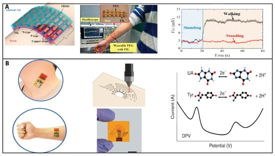
Figure 3. Thermoelectric sensing and electrochemical sensing. (
A) Wearable thermoelectric generators (TEGs) are attracting interest due to their ability to self-power these electronic devices or sensors by harvesting human body heat. Wang et al. developed a numerical model to investigate the performance of wearable TEGs on the curved human wrist. (
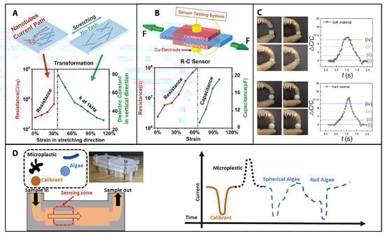
B) Combining microfluidics and laser-engraved fabrication methods, Yang et al. developed a wearable sensor for sensitive detection of uric acid and tyrosine in sweat.
2.5. Acoustic Sensing
Acoustic sensing refers to the use of technology to detect, analyze, and measure sound waves or acoustic signals in various environments and is used to detect a wide range of sounds, from human speech and music to machinery noise and environmental sounds. Acoustic sensing technology typically consists of a sensor that can detect sound waves and can convert them into an electrical signal, which is then processed and analyzed using specialized software or hardware. The sensor may be a microphone or a more complex device, such as an acoustic resonator or a piezoelectric sensor.
Recent advances in nanomaterial-enabled acoustic devices have greatly improved the sensitivity, tunability, and other limitations of conventional acoustic sensors; however, further exploration of flexible acoustic devices is a key priority and will have a great impact on the advancement of intelligent robot–human interaction and flexible electronics
[75]. Wei et al. presented a review of nanomechanical resonators, which are able to detect very small changes in acoustic waves
[76]. The coupling of micro- or nanomechanical resonators via a shared substrate is intensively exploited to build systems for fundamental studies. This can be exploited to realize high-quality phonon cavities, an alternative to acoustic radiation shielding, acoustic superlenses, waveguides, vibration attenuation, mass sensing, and phononic graphene
[77].
Other applications use nanowire-based acoustic sensors, which are a type of sensor that incorporates nanowires. A soft resistive acoustic sensor based on suspended nanowires has also been developed for future wearable voice recognition devices, cochlear implants, and human–machine interfaces
[78]. A flexible, localized acoustic sensor with a mass block-beam using silver nanowires coated on polydimethylsiloxane (PDMS) has also been designed to test the sound source orientation
[79]. Nanowire-based sensors have been studied in the context of 1D nanostructures, nanowire synthesis for sensing, and composite nanowire materials to determine the freshness status of mackerel fish (
Scomber scombrus) in a quick and noninvasive way
[80]. In terms of fabrication, nanocrystalline diamonds are ideal materials for manufacturing various microelectromechanical devices and mass sensors due to their high-frequency working range and excellent material properties. Recently, a low-cost method to fabricate diamond-based micro-resonators using a modified home/office desktop inkjet printer was used to locally deposit nanodiamond ink as
50–60
μ m spots
[81].
2.6. Electrochemical Sensing
Electrochemical sensing is a technique that uses electrochemical principles to detect and measure the concentration of a specific chemical species in a sample. Electrochemical sensors typically consist of a three-electrode cell: an interrogating electrode, a reference electrode, and a counter electrode. A signal is generated within the electrochemical cell and then measured and analyzed by a potentiostat
[82]. Nanotechnology has brought significant progress to the field of electrochemical sensing by enabling the development of highly sensitive and selective sensors with improved performance characteristics.
One of the main advantages of nanotechnology in electrochemical sensing is the ability to increase the surface area of the electrode, which enhances the sensitivity and selectivity of the sensor. This can be achieved by using nanomaterials such as carbon nanotubes, graphene, and metal nanoparticles to modify the electrode surface
[82].
Nanotechnology has also enabled the development of new sensing mechanisms, such as surface-enhanced Raman spectroscopy (SERS) and electrochemiluminescence (ECL), which offer high sensitivity and selectivity for certain analytes
[18].
Recent advancements in electrochemical sensors include the development of microfluidic-based electrochemical sensors for sensing foodborne pathogens
[18], advances in electrochemical sensing platforms enabling the detection of biomolecules and whole cells
[23], and the integration of a flexible electrochemical sensor into a microfluidic chip for simulating and monitoring vascular mechanotransduction
[83].
For other applications, various nanomaterials, such as carbon nanotubes, graphene, and metal nanoparticles, have been integrated into electrochemical sensors to enhance their performance, such as sensitivity, selectivity, and stability
[24][84][85][24,84,85].
For wearable applications, electrochemical sensors have been developed using microfluidics and nanotechnology to monitor various physiological parameters, such as glucose, lactate, and pH in real time and even lead and cadmium from a sample sweat
[86]. These sensors are noninvasive and comfortable to wear, and some can transmit data wirelessly to a smartphone or a cloud server, as discussed by
[87][88][87,88].
On the other hand, paper-based electrochemical sensors have been developed using microfluidics and nanotechnology for point-of-care diagnosis in resource-limited settings. These sensors are low-cost and portable and can detect various analytes, such as glucose, cholesterol, and DNA. Recent advancement are ePADs (electrochemical paper-based analytical devices), including several preparation methods
[31] and printed paper-based electrochemical sensors for low-cost point-of-care disease and environmental diagnostics
[32]. The development of electrochemical and optical detection methods based on microfluidic paper-based analytical devices (
Pads) for point-of-care testing applications is discussed by Hou et al.
[33]. Combining microfluidics and laser-engraved fabrication methods, Yang et al. developed a wearable sensor for the sensitive detection of uric acid and tyrosine in sweat
[34]. See
Figure 3B.
Lastly, multiplexed electrochemical sensors have been developed using microfluidics to detect multiple analytes simultaneously. These sensors can be used for the high-throughput screening of samples and can reduce the cost and time required for analysis
[88]. Multiplexing sensing refers to the simultaneous detection of multiple analytes using a single sensor platform. This approach offers several advantages, such as reduced analysis time, increased throughput, and cost-effectiveness compared to traditional single-analyte detection methods
[34]. Multi-analyte electrochemical detection can enhance the efficiency of analyzing multiple food safety hazards. However, interference and cross-reactions among analytes can impede simultaneous detection by electrochemical sensors. This interference can arise from similar analytes, interferences between channels, and low detection sensitivity. To address these challenges, different nanostructuring options can be employed. These include incorporating nanoparticles to enhance electrocatalytic properties, utilizing nanostructured electrodes to improve sensitivity and selectivity, depositing nanostructured films or coatings to enhance selectivity and stability, incorporating nanopores or nanochannels for controlled analyte diffusion, and employing nanostructured catalysts to enhance electrochemical reactions. These nanostructuring approaches mitigate interference and improve the performance of electrochemical sensors in the simultaneous detection of analytes
[89][90][91][92][89,90,91,92]. Some recent advancements in multiplexing sensing include the development of an antifouling coating that enables affinity-based electrochemical biosensing in complex biological fluids
[93].
Overall, these advancements in electrochemical sensors hold promise for a wide range of applications in healthcare, environmental monitoring, food safety, and many other areas.
2.7. Optical Sensing
Optical sensing refers to the process of detecting and measuring light or other forms of electromagnetic radiation using specialized sensors or devices. Optical sensing works by detecting changes in the intensity, wavelength, polarization, phase, or direction of light or other forms of electromagnetic radiation. Common types of optical sensors include photodiodes, phototransistors, photovoltaic cells, and charge-coupled devices (CCDs).
2.7.1. Photodetection Sensing
A photodetector (PD) is an optoelectronic device that converts incident light or other electromagnetic radiation in the UV, visible, and infrared spectral regions into electrical signals
[94]. Nanotechnology has brought recent progress to photodetection sensing by enabling the development of low-dimensional photodetectors
[95] and nanostructured photodetector technology for UV sensing and pollution detection
[96]. There are also recent developments in lead-free double perovskites for X-ray and UV-vis photodetection
[97].
Graphene and semiconductor nanocrystals have been used in the development of photodetectors due to their unique optical and electronic properties, such as high absorption coefficients and high charge carrier mobility. In this context, nanostructured materials have been developed, such as perovskites, which have a long carrier lifetime, high carrier mobility, and facile synthesis
[98]. Low-dimensional semiconductor/Si hybrid heterostructures provide a great platform for fabricating high-performance photodetectors
[99]. Various absorber materials, such as quantum dots (QDs), plasmonic metal nanoparticles, perovskites, and organic materials, have been investigated to improve broadband absorption
[100].
2.7.2. Plasmonic Nanosensors
Microdevices and nanotechnology have had a significant impact on the field of optical sensing by enabling the development of more sensitive and selective sensors with higher resolution and faster response times. The use of nanoscale materials, advanced fabrication methods, and surface plasmon resonance (SPR) in plasmonic nanosensors has enabled the development of highly sensitive and selective sensing technologies for a wide range of applications, including biomedical diagnostics, environmental monitoring, and food safety
[101][102][101,102].
SPR is a phenomenon that occurs when light interacts with a thin metal film or nanoparticle at a specific angle, causing the conduction electrons in the metal to oscillate and generate an electromagnetic field known as a surface plasmon. This electromagnetic field is highly sensitive to changes in the refractive index of the surrounding environment, making SPR a popular technique for sensing applications
[103].
Plasmonic biosensors use evanescent waves to detect analytes such as proteins, nucleic acids, pathogens, and drugs without the need for labeling. This label-free detection provides exceptional sensitivity in a real-time one-step format
[104].
Plasmonic nanosensors take advantage of the SPR phenomenon to detect changes in the environment. By functionalizing metal nanoparticles with specific biomolecules or chemical groups, plasmonic nanosensors can detect the presence of specific analytes or molecules in a sample. The interaction between the analyte and the functionalized nanoparticles causes a shift in the SPR signal, which can be measured to determine the concentration or presence of the analyte
[25].
Recent advancements in surface plasmon resonance (SPR) include the development of highly sensitive pathogen biosensing techniques
[105]. There have been significant developments in SPR sensing devices for the detection of various chemical and biological molecules
[26]. A review by Huo et al. describes the principle of SPR imaging and discusses recent developments in prism-coupled and non-prism-coupled SPRI techniques in detail
[106].
Knoezer et al. demonstrated how an optical frequency comb can be used to enhance the functionality of an integrated photonic biosensor platform by sampling the spectral response of a Mach–Zehnder interferometer and arranging the sample response to periodic intervals to combine them into a single measurement of the interferometer phase, resulting in a lower limit of detection of 3.7 × 10
RIU
[107].
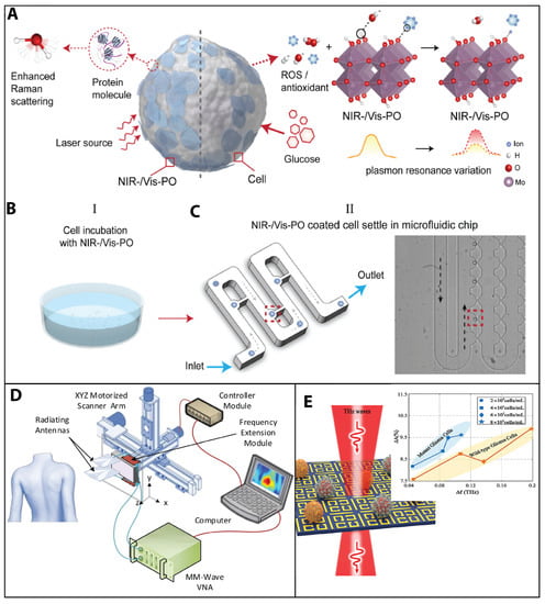
In another application, a dual-functional nanoprobe based on dopant-driven plasmonic oxides was recently developed, demonstrating a maximum accuracy above
90% in distinguishing single THP-1 cells (related to leukemia) from peripheral blood mononuclear cells (PBMCs) and human embryonic kidney (HEK) 293 cells from the human macrophage cell line U937 based on their surface-enhanced Raman spectroscopy (SERS) patterns
[108]. See
Figure 4A.
Lastly, in terms of the tunability of materials, nanoscale materials are commonly used in plasmonic nanosensors to tune the plasmonic properties of the material and increase sensitivity. Researchers can control the size, shape, and composition of nanoparticles to optimize sensor performance, and the high surface-area-to-volume ratio of nanoscale materials allows for their functionalization. Two-dimensional nanomaterials such as graphene and transition metal dichalcogenides have been studied for their potential to improve SPR sensor performance with increased sensitivity and narrower full-width half-maxima
[26]. Similarly, metal–organic frameworks provide many attractive features, including tailorable porosity, high surface areas, good chemical/thermal stability, and various host–guest interactions, making them appealing candidates for volatile organic compound capture and sensing
[109].
Figure 4. Optical sensing and electromagnetic wave technology. (
A–
C) Single-cell analysis using a dual-functional nanoprobe based on dopant-driven plasmonic oxides, which enables the identification of a single THP-1 (related to leukemia) cells from peripheral blood mononuclear cells (PBMCs) and human embryonic kidney cells from human macrophage cells based on their surface-enhanced Raman spectroscopy (SERS) patterns. (
B,
C) (I) Cells are coated with PO (plasmonic oxide) via incubation. (II) Illustration (
left) and optical image (
right) of the PO-coated cells infused into a microfluidic chip and settled separately in the small grooves (highlighted in red). (
D) Millimeter-wave technology. Schematic of the developed ultra-wideband millimeter-wave imaging system for real-time in vivo skin cancer imaging, achieving an overall synthetic bandwidth of 98 GHz. At each scanning step, two sub-band antennas are placed in front of the target, transmit their signals in their respective sub-band frequency ranges, and record the backscattered signals. (
E) Metamaterial-inspired biosensors using THz detection and a label-free biosensing approach for molecular classification of glioma cells. A metamaterial biosensor consisting of cut wires and split-ring resonators is used to realize polarization-independent electromagnetically induced transparency (EIT) at THz frequencies. The theoretical sensitivity of the biosensor was evaluated up to 496.01 GHz/RIU. The measured results indicated that mutant and wild-type glioma cells can be distinguished directly by observing variations in both the EIT resonance frequency and magnitude at any cell concentration without antibody introduction.
2.7.3. Photonic Crystals
Photonic crystals are periodic structures with a periodicity on the order of the wavelength of light. By controlling the periodicity and composition of photonic crystals, it is possible to create sensors that are highly sensitive to changes in the refractive index of a sample. For example, photonic crystal sensors have been used to detect small changes in the concentration of glucose in blood samples
[110][112]. The sensor is able to perform at an ultrahigh sensitivity of 4200 nm/RIU, is a low-cost, tunable design, enables real-accurate detection, and has a simple structure, which is supportive of an industrial design using low-cost product nanofabrication techniques. On the other hand, Boes et al. presented an excellent review of lithium niobate, showing its capabilities to open a new-generation field in sensor development due to its virtues, such as a large dynamic range
[111][113]. Additionally, integrated photonics on thin-film lithium niobate holds great promise for realizing low-cost and scaled optical solutions for communication, sensing, and computation
[111][113].
Overall, nanotechnology has allowed for the development of optical sensors with higher sensitivity, selectivity, and resolution, making them valuable tools for a wide range of applications, from biomedical diagnostics to environmental monitoring.