Voltage surge protection devices (SPDs) or surge arresters rely on metal oxide varistors (MOVs) to safeguard electrical equipment in consumer electronics and industrial electric power systems against the destructive temporary overvoltages (TOVs) resulting from transient switching surges or lightning strikes. The primary function of voltage-sensitive MOVs in SPDs is to prevent the damage caused by high-energy transients by clamping or eliminating them when a surge occurs. These MOVs are mounted in parallel with the components that they are designed to protect.
- metal oxides
- ceramic materials
- ZnO-V2O5-based varistors
- powder metallurgy route
- functional properties
1. Introduction
Table 1.
Critical parameters and functions of MOV devices (adapted from
[52]
).
| ||||||||||
|
| |||||||||
|
|
|
|
Parameter | Function | Comments | Reference | ||||||||
|---|---|---|---|---|---|---|---|---|---|---|---|
Nonlinear coefficient (α) | Protective level | Typical α values in the low-current region are 20–70. | |||||||||
Nonlinear voltage (V) | Voltage rating | It is the threshold or breakdown voltage (VB) at a current of 1 mA. | |||||||||
Leakage current (IL) | Watt loss/operating voltage | DC IL values ≤ 100 μA for small-sized MOV discs, and ≤200 μA for large-sized MOV discs equipping electric power and telecommunication SPDs; AC IL = IR + IC. | |||||||||
Lifetime | Stability | Generated power (PG) < dissipated power (PD). | [52] | ||||||||
Energy absorption capability (E) | Survival of the electrical components | E depends on the size of MOV discs; a high surface-to-volume ratio of the MOV discs leads to a high E. |
Reliable MOVs have to exhibit high nonlinearity (α) and energy absorption capability, a low leakage current (IL) or leakage current density (JL), and long-term stability [56]. Low IL and JL values can avoid thermal runaway, while satisfactory stability and aging behavior are preserved, besides reduced electric power consumption [5]. However, we do not expect MOVs with the highest nonlinearity to have the highest energy absorption capability [56]. Furthermore, high EB can improve surge protection and ensure the reduction of the device size in HV power systems. Nonetheless, the EB increase can decrease the nonlinearity (α) and increase IL and JL. Therefore, state-of-the-art studies of ZnO-based varistors commonly report values of α < 60, JL > 1 μA/cm2, and EB of 2–5 kV/cm [5].
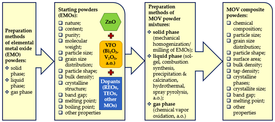
2. Preparation Methods of Elemental MOs and Composite Powders for MOVs
Preparation Methods of EMO and MOV Powders | Advantages | Disadvantages | ||||||
|---|---|---|---|---|---|---|---|---|
|
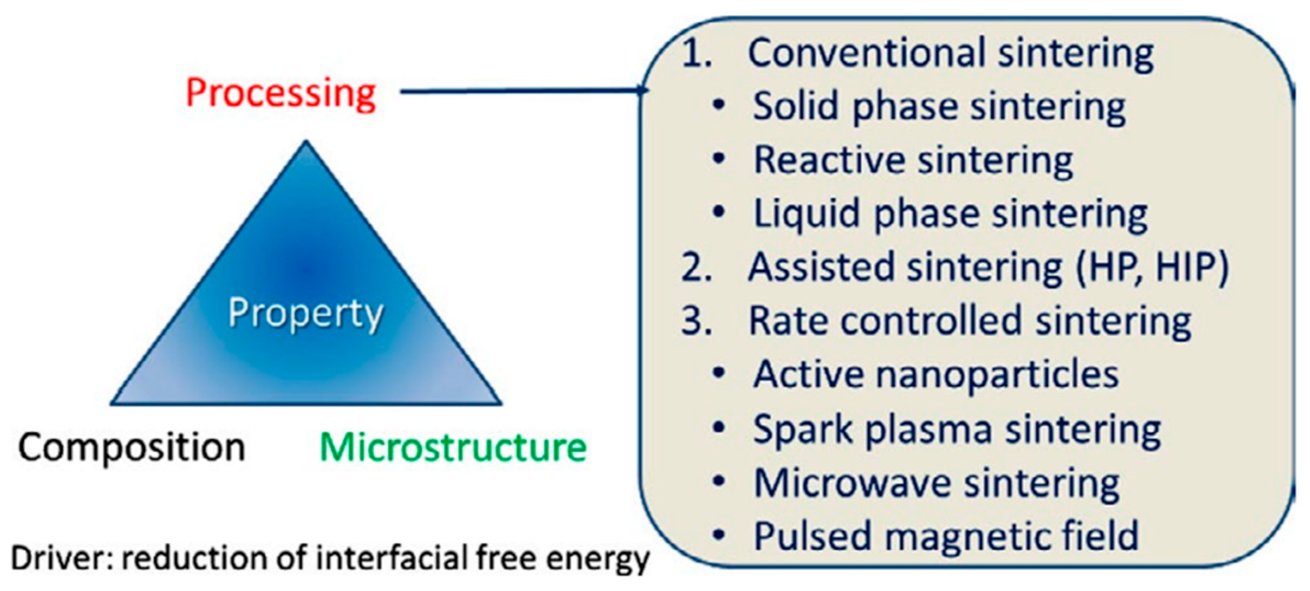
3. Preparation Methods and Major Assessment Criteria of ZnO-Based MOVs
- ➢
-
conventional sintering (CS), which includes solid-phase sintering (CS-SPS), reactive sintering (CS-RS), and liquid-phase sintering (CS-LPS);
- ➢
-
assisted sintering involving hot pressing (HP) or hot isostatic pressing (HIP);
- ➢
-
rate-controlled sintering (RCS) by using (i) active nanoparticles (NPs); (ii) spark plasma sintering (SPS), which is an electric-field-assisted process; (iii) microwave sintering (MWS), or (iv) pulsed magnetic field (PMF) processes.
-
4. Liquid-Phase Sintering (LPS) of ZnO-Bi2O3- and ZnO-V2O5-Based Systems
5. Polymorphisms of Bi2O3 and V2O5
6. Crystallographic Defects and Doping of ZnO
Crystallographic defects are essential characteristics in designing MO semiconductors, such as ZnO, TiO2, SnO2, In2O3, and so on [95][96]. In multicomponent ZnO-based varistors, bulk, surface, and interfacial defects can occur between ZnO and multiple MO additives. The interfacial defects are similar to the surface defects, and can be composed of point defects (vacancies and foreign metal doping), volume defects (voids and disorders), or end of line defects (screw or edge dislocations), as well as planar defects (GBs and twin boundaries) [95]. Grain boundaries are the most commonly reported planar defects in ZnO, along with point defects. The primary native defects found in ZnO are Zn vacancies (VZnO), O vacancies (VO), Zn interstitials (Zni), O interstitials (Oi), Zn antisites (ZnO), and O antisites (OZn). In Zn antisites, Zn can substitute for O, while, in O antisites, O can substitute for Zn. Kröger–Vink notation is the standard notation for defects in ionic crystals, and an example of defect formation in ZnO-V2O5-based systems is given in reference [97]. A ZnO semiconductor usually has an n-type structure in which negatively charged electrons (e−) are the majority charge carriers, while positively charged holes (h+) are the minority charge carriers. The n-type conductivity of semiconductors is caused by structural point defects (vacancies and interstitials) and extended defects (surface conduction, dislocations, stacking faults, and grain boundaries) [98]. The factors related to the dopants, such as their formation and ionization energy, and the solubility of dopants, define the effects of MO doping on ZnO semiconductors [99]. In multicomponent ZnO-based varistors, each introduced dopant in the host lattice of the ZnO crystal structure can act as a donor (e.g., Y ions from Y2O3, Mn ions from Mn3O4) [23][35][100] or an acceptor (e.g., Mn ions from MnO2) [100], or both (e.g., Mn ions with various valence states) [100], depending on the ionic radius and relative valency of the guest (dopant) metal ions and host (ZnO) ions [11]. Adding insoluble MOs such as Bi2O3, In2O3, Cr2O3, NiO, Nb2O5, and Ta2O5, among others, and REOs (e.g., Dy2O3, La2O3, Gd2O3, Nd2O3, Er2O3, Y2O3, Sm2O3, etc.) with a larger ionic radius than that of ZnO can generate varistor behavior in ZnO-based systems. This addition causes the metal oxides to segregate at the ZnO GB regions and create donor states to enhance electron conduction among n-type ZnO grains [101][102]. MOs with lower ionic radii than that of ZnO, such as CoO, Mn3O4, MnO2, V2O5, Ga2O3, and others, are also added to ZnO-based systems to improve their electrical properties. This is achieved by forming more donor states, which enhances electron conduction and increases the nonlinearity of the varistors. The reduction of the leakage current occurs by decreasing the number of defects in the MOVs caused by the reduced ionic radii of the MO dopants. In ZnO-based MOVs, the nonlinear behavior is attributed to the presence of GBs in the polycrystalline ceramic materials. The GBs act as barriers for current flow and can be considered as a network of DSBs and/or ohmic contacts. The composition and distribution of metal impurities and dopants at the GBs affect the potential barrier height and width, which, in turn, determines the electrical properties of the varistors. The difference between the ZnO-V2O5 and ZnO-Bi2O3 systems in GBs lies in the distribution of the dopant, either vanadium (V5+) or bismuth (Bi3+), within the ZnO-based varistor material. In the ZnO-V2O5 system, vanadium (V5+) is incorporated into the GBs in such a way that leads to the formation of donor states, since the ionic radius of V2O5 (0.054 nm) is lower than that of ZnO containing Zn2+ (0.06 nm) [103]. These donor states can trap electrons, leading to a nonlinear response of the ZnO-V2O5 varistor material to an applied voltage. On the other hand, in the ZnO-Bi2O3 system, bismuth (Bi3+) is distributed more uniformly throughout the GBs since the ionic radius of Bi2O3 (0.103 nm) is larger than that of ZnO containing Zn2+ (0.06 nm) [103]. Therefore, the resulting ZnO-Bi2O3 varistor material has a different nonlinear response. To control the ZnO grain growth during sintering and improve the performance of MOVs, binary ZnO-Bi2O3 systems are doped with grain growth modifiers or spinel-forming dopants such as Sb2O3, SnO2, TiO2, In2O3, Mn3O4, Al2O3, and Sb2O5, among others, with oxidation states (+III, +IV, +V) greater than +II of ZnO with Zn2+ ions [44][50][73][104][105][106]. These dopants enhance the donor states and reduce the barrier height at the GBs, which further improves the electrical performance of MOVs. The introduction of spinel-forming dopants into the ZnO crystal structure results in growth defects, such as inversion boundaries (IBs), which show inverted c-axis polarity across distinct crystal planes in ZnO grains [44][50][73][104][107]. Nonetheless, IBs do not form in pure ZnO crystal [50]. Researchers have reported two main IB nucleation mechanisms for ZnO-based varistors doped with IB-forming dopants [73][104]. The first IB nucleation mechanism occurs for dopants with a +III oxidation state and is governed by Zn vacancy (VZn) diffusion. On the other hand, all IB-forming dopants exhibit the second IB nucleation mechanism, which is based on surface nucleation and growth. This mechanism is governed by the chemisorption of the IB-forming dopants on Zn-deficient (0001) basal surfaces of the wurtzite ZnO crystal structure [73]. The solid-state reaction between ZnO and IB-forming dopants generates IBs at lower temperatures and activation energies than those of the spinel phase origination. Low content (e.g., 0.1 mol.%) of IB-forming dopants creates a small number of IB nuclei and a coarse-grained microstructure. Conversely, high content (≥2 mol.%) of IB-forming dopants creates an increased number of IB nuclei and a fine-grained microstructure [73]. The existence of IBs in commercial ZnO-based varistors results in enhanced varistor properties [107]. These IBs cross virtually every ZnO grain feature, predominantly the C− planes in the GBs, and improve the I-V characteristics. Higher reactivity between the Bi2O3-rich liquid phase and the solid ZnO phase in the vicinity of the IB-forming dopant can improve ZnO grain growth in ZnO-Bi2O3-based systems. The IB-forming dopant/Bi2O3 ratio determines the phase equilibrium and the temperature of Bi2O3-rich liquid-phase generation. However, the effect of IB-forming dopants in ZnO-V2O5-based systems is scarcely addressed.7. Electrical Properties of the Selected ZnO-Based Systems
Figure 3, Figure 4 and Figure 5 present the variations in the breakdown field (EB), nonlinear coefficient (α) in the low-current region, and leakage current density (JL) with the sintering temperature of MOVs from ZnO-0.5 mol.% V2O5-based systems.
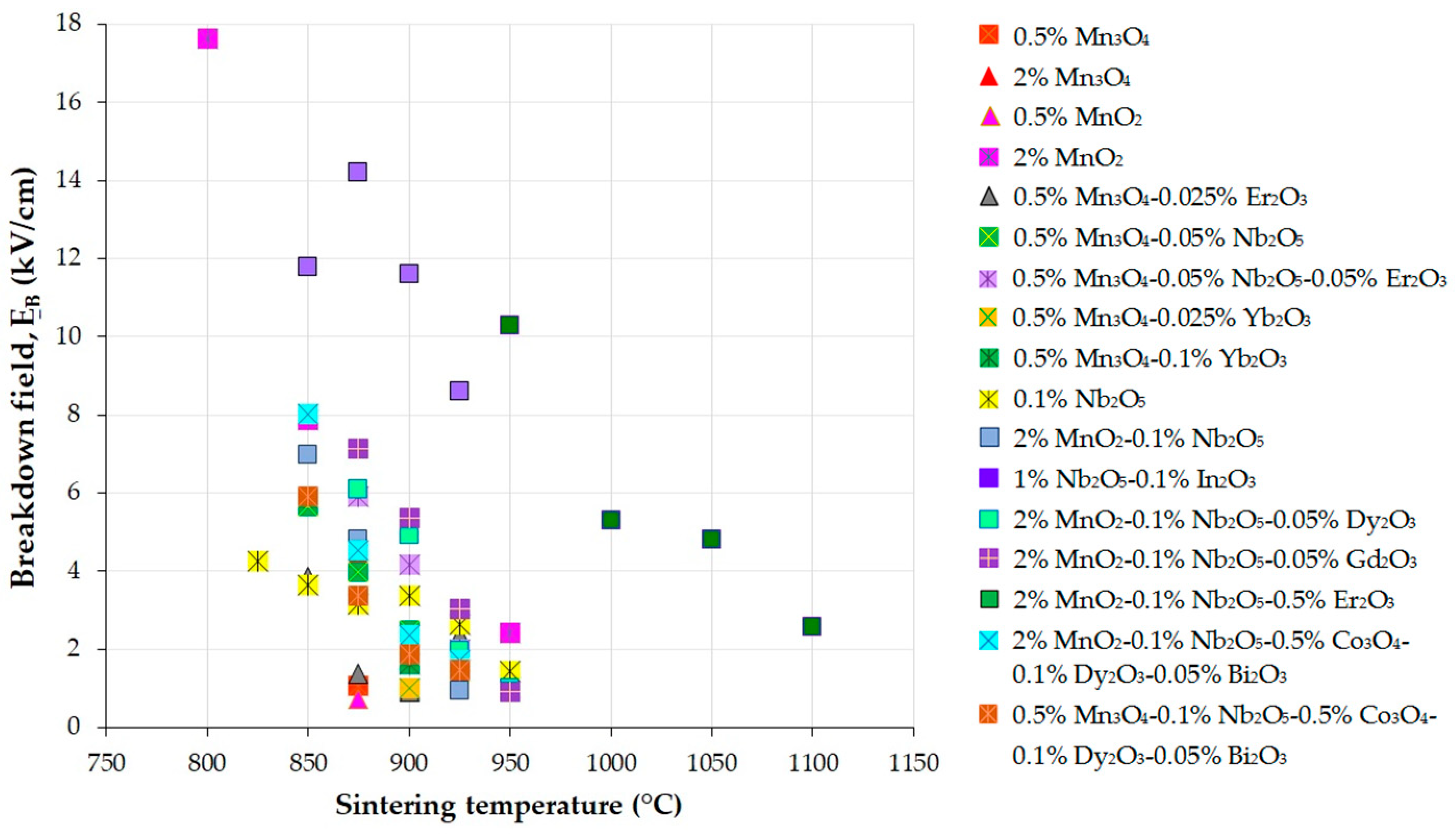
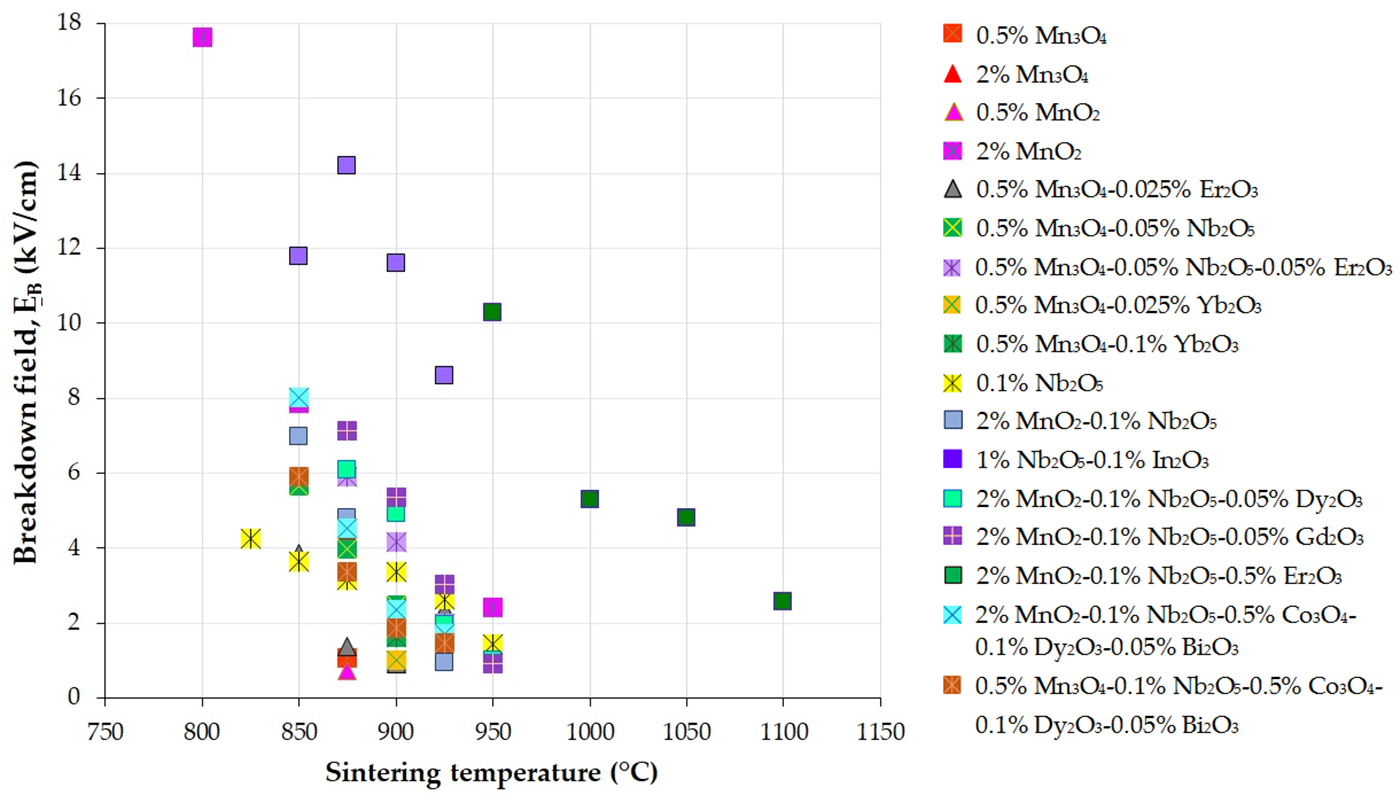
Figure 3. Variation in the breakdown field (EB) with the sintering temperature of MOVs from the ZnO-0.5 mol.% V2O5-based systems doped with various MOs (mol.%). The data plotted in the figure were collected from references [24][33][41][82][100][108][109][110][111][112][113][114][115][116].
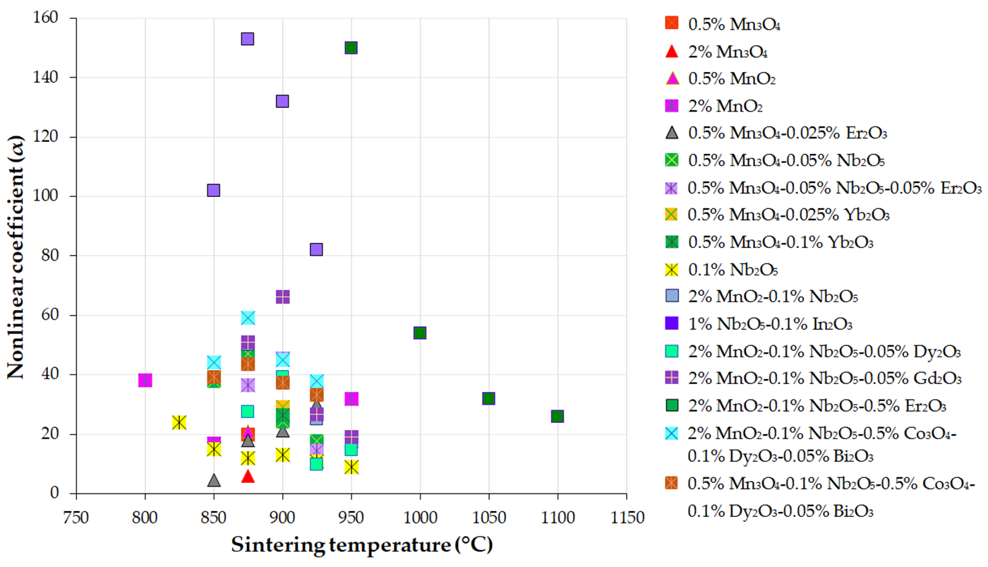
Figure 4. Variation in the nonlinear coefficient (α) in the low-current region with the sintering temperature of MOVs from the ZnO-0.5 mol.% V2O5-based systems doped with various MOs (mol.%). The data plotted in the figure were collected from references [24][33][41][82][100][108][109][110][111][112][113][114][115][116].
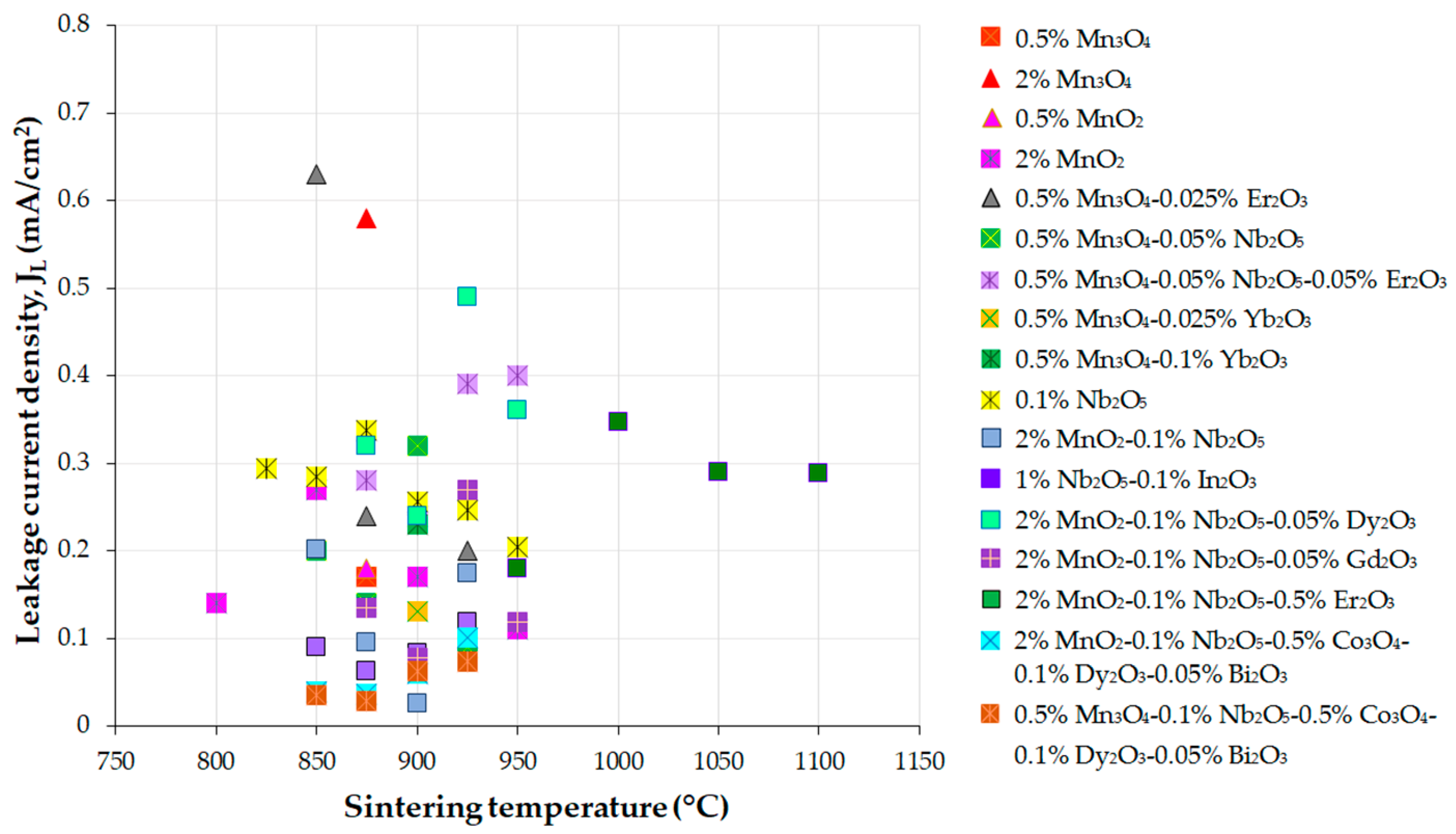
 Figure 5. Variation in the leakage current density (JL) with the sintering temperature of MOVs from the ZnO-0.5 mol.% V2O5-based systems doped with various MOs (mol.%). The data plotted in the figure were collected from references [24][33][41][82][100][108][109][110][111][112][113][114][115][116].
The decrease in EB with an increase in sintering temperature (Figure 3) is attributed to the reduction in the number of GBs across the thickness of the MOV disc due to the increase in the mean ZnO grain size and the corresponding decrease in the breakdown voltage drop per GB [33][35][41][81][109][117][118]. In contrast, the increase in EB is caused by the decrease in the mean ZnO grain size, leading to an increase in the number of GBs [119].
The nonlinearity (α) of the MOVs from the ZnO-based systems is greatly dependent on the electrical potential barrier height (ΦB) at the GBs. ΦB is expressed as the absolute value of the difference between the Fermi energy levels in the GB (EFB) and the ZnO grains (EFG) (EFB < EFG) [5].
During the sintering process of ZnO-based systems, point defects occur at the GBs, which relocate the EFB to a higher position in the band gap energy (Eg). This shift in EFB creates DSBs (depletion zones at either side of the GBs), resulting in the formation of potential barriers [5][46]. Furthermore, changes in the sintering temperature can modify the interface state density (Ns) at the GBs, causing the defect ions (native or additive donors) to move toward the GBs and generate more active GBs [113].
Doping ZnO grains with small amounts of MOs (e.g., MnO2, Mn2O3, In2O3, Sb2O3, Cr2O3, etc.), in ZnO-based systems, can increase the Fermi energy levels in the ZnO grains (EFG), causing a shift in the band gap energy (Eg). This leads to an improvement in ΦB, resulting in better nonlinearity (higher α) and a lower IL or JL compared to pure n-type ZnO semiconductors with a direct Eg of ~3.37–3.4 eV at RT [2][96][120], which exhibit very low nonlinearity and almost equal Fermi energy levels in the GBs and ZnO grains [5].
The enhancement in nonlinearity (α) with increasing sintering temperature (Figure 4) was attributed to the variation in the Schottky barrier height, which changes with the electronic states at the GBs during sintering when defect ions are promoted near the GBs [112]. Therefore, the decrease in the ΦB at the GBs led to the reduction in the α values as the sintering temperature varied [113].
Table 3 demonstrates that ZnO-V2O5 systems with lower amounts of MO additives exhibit comparable or even superior electrical characteristics to the selected ZnO-Bi2O3-based systems when sintered at lower temperatures. This suggests that manufacturers can use less MO dopants and lower sintering temperatures to produce high-performance ZnO-V2O5-based varistors, leading to savings in raw materials and energy costs [73].
Table 3. Critical electrical parameters of MOV devices from several ZnO-V2O5-based systems with good varistor properties compared to those of some relevant ZnO-Bi2O3-based systems.
Figure 5. Variation in the leakage current density (JL) with the sintering temperature of MOVs from the ZnO-0.5 mol.% V2O5-based systems doped with various MOs (mol.%). The data plotted in the figure were collected from references [24][33][41][82][100][108][109][110][111][112][113][114][115][116].
The decrease in EB with an increase in sintering temperature (Figure 3) is attributed to the reduction in the number of GBs across the thickness of the MOV disc due to the increase in the mean ZnO grain size and the corresponding decrease in the breakdown voltage drop per GB [33][35][41][81][109][117][118]. In contrast, the increase in EB is caused by the decrease in the mean ZnO grain size, leading to an increase in the number of GBs [119].
The nonlinearity (α) of the MOVs from the ZnO-based systems is greatly dependent on the electrical potential barrier height (ΦB) at the GBs. ΦB is expressed as the absolute value of the difference between the Fermi energy levels in the GB (EFB) and the ZnO grains (EFG) (EFB < EFG) [5].
During the sintering process of ZnO-based systems, point defects occur at the GBs, which relocate the EFB to a higher position in the band gap energy (Eg). This shift in EFB creates DSBs (depletion zones at either side of the GBs), resulting in the formation of potential barriers [5][46]. Furthermore, changes in the sintering temperature can modify the interface state density (Ns) at the GBs, causing the defect ions (native or additive donors) to move toward the GBs and generate more active GBs [113].
Doping ZnO grains with small amounts of MOs (e.g., MnO2, Mn2O3, In2O3, Sb2O3, Cr2O3, etc.), in ZnO-based systems, can increase the Fermi energy levels in the ZnO grains (EFG), causing a shift in the band gap energy (Eg). This leads to an improvement in ΦB, resulting in better nonlinearity (higher α) and a lower IL or JL compared to pure n-type ZnO semiconductors with a direct Eg of ~3.37–3.4 eV at RT [2][96][120], which exhibit very low nonlinearity and almost equal Fermi energy levels in the GBs and ZnO grains [5].
The enhancement in nonlinearity (α) with increasing sintering temperature (Figure 4) was attributed to the variation in the Schottky barrier height, which changes with the electronic states at the GBs during sintering when defect ions are promoted near the GBs [112]. Therefore, the decrease in the ΦB at the GBs led to the reduction in the α values as the sintering temperature varied [113].
Table 3 demonstrates that ZnO-V2O5 systems with lower amounts of MO additives exhibit comparable or even superior electrical characteristics to the selected ZnO-Bi2O3-based systems when sintered at lower temperatures. This suggests that manufacturers can use less MO dopants and lower sintering temperatures to produce high-performance ZnO-V2O5-based varistors, leading to savings in raw materials and energy costs [73].
Table 3. Critical electrical parameters of MOV devices from several ZnO-V2O5-based systems with good varistor properties compared to those of some relevant ZnO-Bi2O3-based systems.
MOV System Type | State | Pp, Ts/DT | EB | α | IL | JL | MOV Producers | Reference | ||||||||||||||||||
|---|---|---|---|---|---|---|---|---|---|---|---|---|---|---|---|---|---|---|---|---|---|---|---|---|---|---|
ZnO-V2O5-based systems | ||||||||||||||||||||||||||
ZnO-0.5% V2O5-0.5% Mn3O4 | Initial | 80 MPa, | 1.07 | 20 | − | 0.170 | Semiconductor Ceramics | [100] | ||||||||||||||||||
Stressed | 0.96 | 11 | − | 0.480 | ||||||||||||||||||||||
ZnO-0.5% V2O5-0.5% Mn3O4 | Initial | 80 MPa, | 0.72 | 27 | − | 0.042 | [100] | |||||||||||||||||||
Stressed | 0.99 | 20 | − | 0.210 | ||||||||||||||||||||||
ZnO-0.5% V2O5-0.5% Mn3O4-0.1% Yb2O3 | Initial | 100 MPa, | 1.64 | 26.3 | − | 0.230 | [24] | |||||||||||||||||||
Stressed | 1.65 | 25.2 | − | − | ||||||||||||||||||||||
ZnO-0.5% V2O5-1% Nb2O5-0.1% In2O3 | Initial | 500 MPa, | 14.2 ± 0.1 | 153 ± 7 | − | 0.062 | Variable Energy | [41] | ||||||||||||||||||
Initial | 500 MPa, | 11.6 ± 0.2 | 132 ± 8 | − | 0.083 | |||||||||||||||||||||
ZnO-0.5% V2O5-0.5% Mn3O4-0.05% Bi2O3 | Initial | 100 MPa, | 6.027 | 31 | − | 0.043 | Semiconductor Ceramics | [81] | ||||||||||||||||||
ZnO-0.5% V2O5-0.5% Mn3O4-0.1% Bi2O3 | Initial | 3.357 | 24.9 | − | 0.052 | |||||||||||||||||||||
ZnO-Bi2O3-based systems | ||||||||||||||||||||||||||
ZnO-1% Bi2O3-1% Sb2O3-0.75% MnO2-1% Co2O3-0.5% Cr2O3-1% Sb2O3, 1.2% SiO2-0.2% Al2O3-0.005-0.02% In2O3 | Initial | ~39 MPa | 3.56–4.34 | 52–60 | − | 0.002–0.004 | State Key Laboratory of Control and Simulation of Power System and Generation Equipment, | [40] | ||||||||||||||||||
ZnO-0.5% Bi2O3-1% Sb2O3-0.5% CoO-0.5% MnO2-0.5% Cr2O3 | Initial | ~33 MPa | 1.35 | 50 | − | − | Matsushita Electric | [3] | ||||||||||||||||||
Initial | 1100 °C/1 min and 850 °C/1 h | 10.7 | 40 | 58 | − | PPG-CEM, Federal University of | [121] | |||||||||||||||||||
Commercial ZNR 10K 270 | Initial | NA | 0.22 | ≤11 | − | 0.070 | Matsushita Electric | [122] | ||||||||||||||||||
Commercial ZNR 10K 470 | Initial | NA | 0.42 | ≤25 | − | 0.013 | ||||||||||||||||||||
Commercial GEMOV 27Z 1 | Initial | NA | 0.27 | ≤16 | − | 0.035 | General Electric Co., USA | |||||||||||||||||||
Commercial (ZnO-Bi2O3 + MO dopants) | Initial | 1095 °C/2.5 h | 1.85 | 27 | 17 | − | Unknown producer | [76] | ||||||||||||||||||
ZnO-Bi2O3-Sb2O3-Co3O4-Mn2O3-NiO-B2O3-Al2O3 | Initial | 95 MPa, | 1.79 | 56 | 3.4 | − | Tridelta Parafoudres S.A. and UMR CNRS-UPSINP, France | [76] | ||||||||||||||||||
8. Strategies to Improve the Characteristics of MOVs
The size of grains and the number of grain boundaries (GBs) in the microstructures of MOVs, along with the intergranular effects, play a crucial role in altering the varistor properties [123][124][125]. However, controlling the grain size and grain size distribution in multicomponent ZnO-based varistors is a challenging task due to the many interdependent MO dopants needed to achieve the desired varistor characteristics [73]. The ZnO grain size determines the electrical breakdown (EB) of MOVs for a specific formulation and thickness of the MOV disc [124]. The number of GBs across the thickness of an MOV disc increases with the reduction in grain size during sintering, which improves the EB. These factors are essential to consider when designing MOVs using ZnO-based systems. The optimum ratio between dopant content (DC) and GB area (S) is a key performance indicator (KPI) in evaluating the electrical properties of MOVs. However, determining the optimal DC/S ratio usually requires experimentation. When the sintering temperature or dwell time is inadequate, the mean ZnO grain size (dZnO) decreases, leading to an increase in the GB area, while an increase in dZnO leads to a decrease in the GB area. An efficient strategy for improving the non-ohmic behavior of multiternary ZnO-based systems consists of developing novel compositions with appropriate types and content of VFO and MO dopants, using adequate PM processing parameters. A better microstructure can be achieved by reducing the ZnO grain size, obtaining a narrow ZnO grain size distribution, and improving the uniformity and long-term stability of electrical potential barriers (DSBs) across the GBs [30][124][126][127]. The use of IB-forming dopants can tailor the microstructure and the electronic and optical characteristics of ZnO-based systems, benefiting from enhanced functional properties at reduced costs [73]. When selecting the optimal sintering conditions for the manufacturing of ZnO-V2O5-based varistors, it is crucial to consider the effect of V2O5 volatility. This factor can significantly impact various characteristics, including the microstructure, the growth of the ZnO grain size, secondary phase formation, sintered density, and GB parameters. The concentration of metal ions in the MO dopants is a critical factor that determines the formation of GB barriers (DSBs) in ZnO-based varistors [102][128]. A suitable concentration of dopants distributed uniformly along the GBs can enhance the varistor performance. Conversely, an uneven or excessive concentration of dopants may destroy the GB barriers and structure, leading to a decline in varistor performance. The precise control of the MO dopant content is essential to achieving the desired properties in MOVs. Defect engineering, such as self-doping with specific point defects or doping with transition, rare element (RE), or other metal ions is a practical approach to develop high-performance ZnO-based varistors with enhanced electrical properties and prolonged stability [30][96]. By introducing controlled imperfections into the crystal lattice of ZnO from MOV compositions, the band gap and electronic arrangement can be tuned, and the content and mobility (µ) of charge carriers can be improved by restraining mobile Zni and simultaneously increasing the VO density. The degradation rate of the MOVs from the ZnO-based systems can be reduced when the Zni density is lower, since Zni represents the major intrinsic point defect species that generates the electrical degradation of MOVs under DC or AC electrical and thermal stresses [129][130]. Additionally, the Zni density is an effective parameter for investigating the electrical degradation of ZnO-based varistors at a macroscopic level. Therefore, microstructural aspects, such as the grain size, number of GBs, electrical potential barriers (DSBs), and defects in the ZnO crystal structure, are considered in the degradation and failure mechanisms of MOVs to explain their protective roles [125].9. Conclusions
- Powder metallurgy techniques are used to prepare advanced ceramic materials from ball-milled composite powders for metal oxide varistors (MOVs) from the ZnO-V2O5 systems with comparable or superior properties to ZnO-Bi2O3 systems, but with fewer dopants.
- ZnO-V2O5-based systems with 0.25–2 mol.% V2O5 and MO additives sintered in air over 800 °C contain a primary phase of ZnO with a hexagonal wurtzite structure and several secondary phases (e.g., Zn3(VO4)2, ZnV2O4, Zn2V2O7, RE-related phases, etc.) that influence the grain growth behavior of ZnO and the performance of MOVs.
- MOVs from the ZnO-based systems doped with 0.5–2 mol.% V2O5, 2 mol.% MnO2 or 0.5 mol.% Mn3O4, and 0.025–0.5 mol.% MOs (Bi2O3, In2O3, Sb2O3, TEOs, and REOs) exhibit a homogeneous microstructure, high density, and superior varistor properties.
- By refining and homogenizing the microstructure of MOVs, the number of grain boundaries (GBs) increases across the thickness of the MOV disc, improving the electrical properties and stability of MOVs by elevating the Schottky barrier height (ΦB) in the GBs.
- MOVs doped with a small amount (0.025–0.5 mol.%) of grain growth inhibitors (REOs, Bi2O3, and In2O3) demonstrate satisfactory electrical properties, including a low leakage current density (JL) of 0.02–0.2 mA/cm2, a high nonlinear coefficient (α) of 22–153, and a high breakdown field (EB) of 2–14 kV/cm.
- Studies on the grain growth kinetics during the liquid-phase sintering (LPS) of ZnO-V2O5 systems have indicated that doped MOVs exhibit a higher kinetic grain growth exponent and apparent activation energy when compared to undoped ZnO ceramics.
- Overall, high-performance MOVs from ZnO-V2O5-based systems have great potential for practical applications.
References
- Karim, A.N.M.; Begum, S.; Hashmi, M.S.J. Role of surface to volume ratio of zinc oxide arrester blocks on the energy absorption capability. IOP Conf. Ser. Earth Environ. Sci. 2013, 16, 012008.
- He, H. Metal oxide semiconductors and conductors. In Solution Processed Metal Oxide Thin Films for Electronic Applications; Cui, Z., Korotcenkov, G., Eds.; Elsevier: Amsterdam, The Netherlands, 2020; pp. 7–30.
- Matsuoka, M. Nonohmic properties of zinc oxide ceramics. Jpn. J. Appl. Phys. 1971, 10, 736–746.
- Chen, B.; Wang, B.; Gao, P.; Zhang, P.; Chen, H. Effects of raw particle size and annealing on microstructure, electrical and mechanical behaviors of ZnO-based varistors. J. Alloys Compd. 2021, 872, 159638.
- Tian, T.; Zheng, L.; Podlogar, M.; Zeng, H.; Bernik, S.; Xu, K.; Ruan, X.; Shi, X.; Li, G. Novel ultrahigh-performance ZnO-based varistor ceramics. ACS Appl. Mater. Interfaces 2021, 13, 35924–35929.
- Li, S.; Li, J.; Liu, W.; Lin, J.; He, J.; Cheng, P. Advances in ZnO varistors in China during the past 30 years—Fundamentals, processing, and applications. IEEE Electr. Insul. Mag. 2015, 31, 35–44.
- Pianaro, S.A.; Bueno, P.R.; Longo, E.; Varela, J.A. A new SnO2-based varistor system. J. Mater. Sci. Lett. 1995, 14, 692–694.
- Lungu, M.V.; Pătroi, D.; Marinescu, V.; Caramitu, A.; Marin, M.; Tălpeanu, D.; Lucaci, M.; Godeanu, P. Preparation and study of the optical, electrical and dielectric characteristics of some disc-shaped tin dioxide-based varistors. Rom. J. Phys. 2022, 67, 610.
- Liao, X.; Peng, F.; Pu, Y.; Cao, S.; Zhu, D. Effects of Dy2O3 on the electrical properties of a (Nb2O5-Dy2O3-SiO2) Co-doped TiO2 varistor. J. Electron. Mater. 2021, 50, 1963–1979.
- Kang, K.; Zhu, H.; Zhu, G.; Deng, S. Influence of annealing atmosphere on varistor property of TiO2–Nb2O5–SrCO3 ceramics. Mater. Sci. Appl. 2021, 12, 461–474.
- He, J. Metal Oxide Varistors: From Microstructure to Macro-Characteristics; Wiley-VCH Verlag GmbH & Co. KGaA: Weinheim, Germany, 2019.
- Chen, G.; Li, J.; Chen, X.; Kang, X.; Yuan, C. Sintering temperature dependence of varistor properties and impedance spectroscopy behavior in ZnO based varistor ceramics. J. Mater. Sci. Mater. Electron. 2015, 26, 2389–2396.
- Zhao, M.; Wang, Y.; Sun, T.; Song, H. Effect of bismuth and vanadium as the varistor forming element in ZnO-based ceramics. J. Mater. Sci. Mater. Electron. 2020, 31, 8206–8211.
- Mirzayi, M.; Hekmatshoar, M.H. Effect of V2O5 on electrical and microstructural properties of ZnO ceramics. Phys. B Condens. Matter. 2013, 414, 50–55.
- Hng, H.-H.; Knowles, K.M.; Midgley, P.A. Zinc vanadates in vanadium oxide-doped zinc oxide varistors. J. Am. Ceram. Soc. 2001, 84, 435–441.
- Cao, W.; Xie, X.; Wang, Y.; Chen, M.; Qiao, Y.; Wang, P.; Zhang, Y.; Liu, J. Effect of Pr6O11 doping on the microstructure and electrical properties of ZnO varistors. Ceram. Int. 2019, 45, 24777–24783.
- Zhang, L.; Liu, W.; Gao, J.; Kong, F.; Li, Y.; Li, S. Effects of the Er2O3 doping on the microstructure and electrical properties of ZnO–Bi2O3 based varistor ceramics. Ceram. Int. 2021, 47, 32349–32356.
- Roy, S.; Roy, T.K.; Das, D. Grain growth kinetics of Er2O3 doped ZnO-V2O5 based varistor ceramics. Ceram. Int. 2019, 45, 24835–24850.
- Nahm, C.-W. Er2O3 doping effect on electrical properties of ZnO-V2O5-MnO2-Nb2O5 varistor ceramics. J. Am. Ceram. Soc. 2011, 94, 3227–3229.
- Nahm, C.-W. Major effects on electrical properties of ZnO–V2O5–MnO2–Nb2O5 ceramics with small Gd2O3 doping changes. J. Alloys Compd. 2013, 578, 132–135.
- Nahm, C.-W. Effect of Dy2O3 doping on microstructure, electrical and dielectric properties of ZnO–V2O5-based varistor ceramics. J. Mater. Sci. Mater. Electron. 2015, 26, 10217–10224.
- Zhao, M.; Li, X.; Li, T.; Shi, Y.; Li, B. Effect of Y2O3, Nd2O3 or Sm2O3 on the microstructure and electrical properties of ZnVMnNbO varistor ceramics. J. Mater. Sci. Mater. Electron. 2019, 30, 450–456.
- Nahm, C.-W. Yttrium doping effect on varistor properties of zinc-vanadium-based ceramics. J. Korean Ceram. Soc. 2018, 55, 504–509.
- Nahm, C.-W. Effect of Yb2O3 addition on varistor properties and aging characteristics of ZnO–V2O5–Mn3O4 system. J. Mater. Sci. Mater. Electron 2018, 29, 2958–2965.
- Roy, T.K.; Bhattacharyya, T.K.; Thakur, S.K. Role of sintering temperature on microstructure and nonlinear electrical properties of 0.1 mol.% Nb2O5 added ZnO–V2O5 varistor ceramics. J. Mater. Sci. Mater. Electron. 2019, 30, 5640–5651.
- Guo, M.; Wang, Y.; Wu, K.; Zhang, L.; Zhao, X.; Lin, Y.; Li, J. Revisiting the effects of Co2O3 on multiscale defect structures and relevant electrical properties in ZnO varistors. High Voltage 2020, 5, 241–248.
- Hng, H.-H.; Knowles, K.M. Microstructure and current-voltage characteristics of multicomponent vanadium-doped zinc oxide varistors. J. Am. Ceram. Soc. 2004, 83, 2455–2462.
- Bai, H.; Li, S.; Zhao, Y.; Xu, Z.; Chu, R.; Hao, J.; Chen, C.; Li, H.; Gong, Y.; Li, G. Influence of Cr2O3 on highly nonlinear properties and low leakage current of ZnO–Bi2O3 varistor ceramics. Ceram. Int. 2016, 42, 10547–10550.
- Jiang, H.; Ren, X.; Lao, X.; Kong, A.; Zhong, M.; Sun, Y.; Wu, Y.; Yao, Z.; Shi, L. Effect of NiO doping on grain growth and electrical properties of ZnO-based varistors. J. Eur. Ceram. Soc. 2022, 42, 3898–3904.
- Guo, M.; Zhao, X.; Shi, W.; Zhang, B.; Wu, K.; Li, J. Simultaneously improving the electrical properties and long-term stability of ZnO varistor ceramics by reversely manipulating intrinsic point defects. J. Eur. Ceram. Soc. 2022, 42, 162–168.
- Saadeldin, M.M.; Desouky, O.A.; Ibrahim, M.; Khalil, G.E.; Helali, M.Y. Investigation of structural and electrical properties of ZnO varistor samples doped with different additives. NRIAG J. Astron. Geophys. 2018, 7, 201–207.
- Pandey, S.; Kumar, D.; Parkash, O. Electrical impedance spectroscopy and structural characterization of liquid-phase sintered ZnO–V2O5–Nb2O5 varistor ceramics doped with MnO. Ceram. Int. 2016, 42, 9686–9696.
- Nahm, C.-W. Effect of sintering temperature on varistor properties and aging characteristics of ZnO–V2O5–MnO2 ceramics. Ceram. Int. 2009, 35, 2679–2685.
- Wu, J.; Li, T.; Qi, T.; Qin, Q.; Li, G.; Zhu, B.; Wu, R.; Xie, C. Influence of dopants on electrical properties of ZnO-V2O5 varistors deduced from AC impedance and variable-temperature dielectric spectroscopy. J. Electron. Mater. 2012, 41, 1970–1977.
- El-Rabaie, S.; Khafagy, A.H.; Dawoud, M.T.; Attia, M.T. Mechanical, microstructure and electrical properties of ternary ZnO–V2O5–Mn3O4 varistor with sintering temperature. Bull. Mater. Sci. 2015, 38, 773–781.
- Nahm, C.-W. Impulse aging behavior of ZnO-V2O5-based varistors with Nb2O5 addition. J. Am. Ceram. Soc. 2011, 94, 1305–1308.
- Singh, J.; Virpal Sharma, S.; Singh, R.C. Effect of Fe2O3 doping on structural properties of ZnO-V2O5 based varistor system. AIP Conf. Proc. 2017, 1832, 120021.
- Xie, P.; Hu, J. Influence of sintering temperature and ZrO2 dopants on the microstructure and electrical properties of zinc oxide varistors. IEEE Access 2019, 7, 140126–140133.
- Xiao, X.; Zheng, L.; Cheng, L.; Tian, T.; Ruan, X.; Podlogar, M.; Bernik, S.; Li, G. Influence of WO3-doping on the microstructure and electrical properties of ZnO-Bi2O3 varistor ceramics sintered at 950 °C. J. Am. Ceram. Soc. 2015, 98, 1356–1363.
- Meng, P.; Hu, J.; Zhao, H.; He, J. High voltage gradient and low residual-voltage ZnO varistor ceramics tailored by doping with In2O3 and Al2O3. Ceram. Int. 2016, 42, 19437–19440.
- Roy, T.K. High nonlinearity in 0.1 mol.% In2O3 added ZnO–V2O5 based varistors prepared at different sintering temperatures. Ceram. Int. 2021, 47, 35152–35159.
- Cheng, K.; Zhao, H.; Zhou, Y.; Xie, Q. B2O3- and Y2O3-doped ZnO varistor ceramics: Enhanced voltage gradient and nonlinear properties for UHV. Mater. Sci. Semicond. Process. 2021, 123, 105590.
- Bai, H.; Zhang, M.; Xu, Z.; Chu, R.; Hao, J.; Li, H.; Gong, Y.; Li, G. The effect of SiO2 on electrical properties of low-temperature-sintered ZnO-Bi2O3-TiO2-Co2O3-MnO2-based ceramics. J. Am. Ceram. Soc. 2017, 100, 1057–1064.
- Bernik, S.; Daneu, N.; Rečnik, A. Inversion boundary induced grain growth in TiO2 or Sb2O3 doped ZnO-based varistor ceramics. J. Eur. Ceram. Soc. 2004, 24, 3703–3708.
- Bernik, S.; Daneu, N. Characteristics of SnO2-doped ZnO-based varistor ceramics. J. Eur. Ceram. Soc. 2001, 21, 1879–1882.
- Danzer, R.; Kaufmann, B.; Supancic, P. Failure of high power varistor ceramic components. J. Eur. Ceram. Soc. 2020, 40, 3766–3770.
- Kularatna, N.; Ross, A.S.; Fernando, J.; James, S. Components used in surge protection circuits. In Design of Transient Protection Systems; Kularatna, N., Ross, A.S., Fernando, J., James, S., Eds.; Elsevier: Amsterdam, The Netherlands, 2019; pp. 29–42.
- Diwald, O. Zinc oxide nanoparticles for varistors. In Metal Oxide Nanoparticles; Diwald, O., Berger, T., Eds.; Wiley: Hoboken, NJ, USA, 2021; pp. 783–807.
- Hasse, L.; Konczakowska, A.; Smulko, J. Classification of high-voltage varistors into groups of differentiated quality. Microelectron. Reliab. 2009, 49, 1483–1490.
- Rečnik, A.; Bernik, S.; Daneu, N. Microstructural engineering of ZnO-based varistor ceramics. J. Mater. Sci. 2012, 47, 1655–1668.
- Eda, K. Zinc oxide varistors. IEEE Electr. Insul. Mag. 1989, 5, 28–30.
- Gupta, T.K. Application of zinc oxide varistors. J. Am. Ceram. Soc. 1990, 73, 1817–1840.
- Simo, A.; Frigura-Iliasa, F.M.; Frigura-Iliasa, M.; Andea, P.; Musuroi, S. Service limits for metal oxide varistors having cylindrical symmetry as function of the ambient temperature. Symmetry 2022, 14, 1351.
- Pillai, S.C.; Kelly, J.M.; Ramesh, R.; McCormack, D.E. Advances in the synthesis of ZnO nanomaterials for varistor devices. J. Mater. Chem. C 2013, 1, 3268.
- Begum, S.; Karim, A.N.M.; Fawzia, S.; Hashmi, M.S.J. Alternative process and design opportunities for ZnO-based surge arrester: An investigation oriented roadmap. In Encyclopedia of Materials: Electronics; Haseeb, A.S.M.A., Ed.; Elsevier: Amsterdam, The Netherlands, 2023; Volume 3, pp. 464–483.
- Huda, D.; El Baradie, M.A.; Hashmi, M.S.J.; Puyane, R. Study of electrical characteristics and microstructure of zinc oxide varistor through rate-controlled sintering. J. Mater. Sci. 1998, 33, 271–278.
- Frigura-Iliasa, F.; Musuroi, S.; Sorandaru, C.; Vatau, D. Case study about the energy absorption capacity of metal oxide varistors with thermal coupling. Energies 2019, 12, 536.
- Chu, S.-Y.; Yan, T.-M.; Chen, S.-L. Analysis of ZnO varistors prepared by the sol–gel method. Ceram. Int. 2000, 26, 733–737.
- Yang, R.; Qu, X.; Wang, M. Sol–gel synthesis of Ba-doped ZnO nanoparticles and its use in varistor ceramics. Micro Nano Lett. 2018, 13, 1506–1509.
- Porcayo-Calderon, J.; Ramos-Hernandez, J.J.; Arrieta-Gonzalez, C.D.; Chacon-Nava, J.G.; Gonzalez-Rodriguez, J.G.; Porcayo-Palafox, E.; Sanchez-Carrillo, M.; Flores-De los Rios, J.P.; Martinez-Gomez, L. Synthesis by hydrothermal treatment of ZnO-based varistors doped with rare earth oxides and their characterization by impedance spectroscopy. Crystals 2020, 10, 1134.
- Strachowski, T.; Baran, M.; Małek, M.; Kosturek, R.; Grzanka, E.; Mizeracki, J.; Romanowska, A.; Marynowicz, S. Hydrothermal synthesis of zinc oxide nanoparticles using different chemical reaction stimulation methods and their influence on process kinetics. Materials 2022, 15, 7661.
- Hembram, K.; Rao, T.N.; Srinivasa, R.S.; Kulkarni, A.R. High performance varistors prepared from doped ZnO nanopowders made by pilot-scale flame spray pyrolyzer: Sintering, microstructure and properties. J. Eur. Ceram. Soc. 2015, 35, 3535–3544.
- Polarz, S.; Roy, A.; Merz, M.; Halm, S.; Schröder, D.; Schneider, L.; Bacher, G.; Kruis, F.E.; Driess, M. Chemical vapor synthesis of size-selected zinc oxide nanoparticles. Small 2005, 1, 540–552.
- Sousa, V.C.; Segadães, A.M.; Morelli, M.R.; Kiminami, R.H.G.A. Combustion synthesized ZnO powders for varistor ceramics. Int. J. Inorg. Mater. 1999, 1, 235–241.
- Kelleher, M.C. ZnO varistors—the ideal microstructure and characteristics, and methods investigated and developed to achieve these. In Encyclopedia of Materials: Electronics; Haseeb, A.S.M.A., Ed.; Elsevier: Amsterdam, The Netherlands, 2023; Volume 3, pp. 392–418.
- Tan, D.Q. Superior performing nano-enabled metal oxide varistors. Int. J. Ceram. Eng. Sci. 2019, 1, 136–143.
- Hassazadeh, M.; Puyane, R.; Malpiece, F. Ecological design up-grade of a zinc oxide varistor suitable for distribution polymeric surge arresters. In Proceedings of the 18th International Conference and Exhibition on Electricity Distribution (CIRED 2005), Turin, Italy, 6–9 June 2005; Volume 2005, p. v1-50.
- Bernik, S. Low-temperature sintering of ZnO-Bi2O3-based varistor ceramics for enhanced microstructure development and current-voltage characteristics. Ceram. Silik. 2017, 62, 8–14.
- Arefin, M.L.; Raether, F.; Dolejš, D.; Klimera, A. Phase formation during liquid phase sintering of ZnO ceramics. Ceram. Int. 2009, 35, 3313–3320.
- Kaufmann, B.; Billovits, T.; Supancic, P. Observation of an electrical breakdown at ZnO Schottky contacts in varistors. J. Eur. Ceram. Soc. 2021, 41, 1969–1974.
- Sendi, R.K. Structural, nonlinear electrical characteristics, and stability against DC-accelerated aging stress behavior of Er-doped 20 nm ZnO–Bi2O3–Mn2O3-based varistors. Microsc. Res. Tech. 2021, 84, 2236–2243.
- Xie, P.; Wang, Z.; Wu, K. Evolution of intrinsic and extrinsic electron traps at grain boundary during sintering ZnO based varistor ceramics. Materials 2022, 15, 1098.
- Daneu, N.; Bernik, S.; Rečnik, A. Inversion boundary induced grain growth in ZnO ceramics: From atomic-scale investigations to microstructural engineering. J. Phys. Conf. Ser. 2011, 326, 012003.
- Kim, J.; Kimura, T.; Yamaguchi, T. Effect of bismuth of oxide content on the sintering of zinc oxide. J Am. Ceram. Soc. 1989, 72, 1541–1544.
- Xu, D.; Cheng, X.; Yan, X.; Xu, H.; Shi, L. Sintering process as relevant parameter for Bi2O3 vaporization from ZnO-Bi2O3-based varistor ceramics. Trans. Nonferrous Met. Soc. China 2009, 19, 1526–1532.
- Izoulet, A.; Guillemet-Fritsch, S.; Estournès, C.; Morel, J. Microstructure control to reduce leakage current of medium and high voltage ceramic varistors based on doped ZnO. J. Eur. Ceram. Soc. 2014, 34, 3707–3714.
- Choi, S.-K.; Jung, H.-H.; Kang, S.-M. The correlation between surge energy capability and Bi2O3 volatilization in ZnO varistors. J. Ceram. Soc. Japan 2018, 126, 236–240.
- Zhu, F.; Liu, C.; Li, J.; Zheng, D.; Pang, C.; Fei, Z. Effect of Zn7Sb2O12 pre-synthesis on microstructure and properties of ZnO varistor ceramics. AIP Adv. 2022, 12, 065214.
- Dugar, J.; Ikram, A.; Pušavec, F. Evaluation of chip formation mechanisms in the turning of sintered ZnO electro-ceramics. Processes 2021, 9, 1422.
- Chen, T.; Zu, H.; Gao, C.; Ke, C.; Zhou, D.; Hu, Y.; Zheng, Z.; Fu, Q. Preparation and electrical properties of ZnO-Bi2O3-based multilayer varistors with base metal nickel inner electrodes. J. Am. Ceram. Soc. 2017, 100, 3024–3032.
- Nahm, C.-W. Effect of Bi2O3 doping on microstructure and electrical properties of ZnO–V2O5–Mn3O4 semiconducting ceramics. J. Mater. Sci. Mater. Electr. 2017, 28, 903–908.
- Nahm, C.-W. Aging Characteristics of ZnO–V2O5-based varistors for surge protection reliability. Microelectron. Reliab. 2014, 54, 2836–2842.
- Hng, H.H.; Knowles, K.M. Characterisation of Zn3(VO4)2 phases in V2O5-doped ZnO varistors. J. Eur. Ceram. Soc. 1999, 19, 721–726.
- Pandey, S.; Kumar, D.; Parkash, O. Investigation of the electrical properties of liquid-phase sintered ZnO–V2O5 based varistor ceramics using impedance and dielectric spectroscopy. J. Mater. Sci. Mater. Electron. 2016, 27, 3748–3758.
- Kurzawa, M.; Rychlowska-Himmel, I.; Bosacka, M.; Blonska-Tabero, A. Reinvestigation of phase equilibria in the V2O5 system. J. Therm. Anal. Calorim. 2001, 64, 1113–1119.
- Wu, J.; Qi, T.; Li, T.T.; Qin, Q.W.; Li, G.Q.; Zhu, B.L.; Xiang, Z.D.; Xie, C.S. The AC impedance and variable temperature dielectric spectroscopic analysis of MnO2 doped and un-doped ZnO–V2O5 ceramics. J. Mater. Sci. Mater. Electron. 2012, 23, 1143–1150.
- Qu, X.; Sun, W.-J.; Wang, M.-H.; Chen, Y.; Zhang, H.-P. Microstructures and electrical properties of ZnO–V2O5–MnO2 varistors with low-temperature sintering. J. Mater. Sci. Mater. Elect. 2017, 28, 1909–1913.
- Klinkova, L.A.; Nikolaichik, V.I.; Barkovskii, N.V.; Fedotov, V.K. Thermal stability of Bi2O3. Russ. J. Inorg. Chem. 2007, 52, 1822–1829.
- Mielcarek, W.; Gubański, A.; Paściak, G.; Prociów, K.; Warycha, J.; Wrobel, J.M. The effect of bismuth oxide polymorph forms on degradation processes in ZnO varistors. Ceram. Int. 2013, 39, 8219–8226.
- He, J.; Cheng, C.; Hu, J. Electrical degradation of double-Schottky barrier in ZnO varistors. AIP Adv. 2016, 6, 030701.
- Cao, W.; Guo, Y.; Su, J.; Liu, J. Effect of sintering temperature on the microstructural evolution of ZnO varistors. J. Electron. Mater. 2023, 52, 1266–1273.
- Parija, A.; Waetzig, G.R.; Andrews, J.L.; Banerjee, S. Traversing energy landscapes away from equilibrium: Strategies for accessing and utilizing metastable phase space. J. Phys. Chem. C 2018, 122, 25709–25728.
- Tadeu Cestarolli, D.; Maria Guerra, E. Vanadium pentoxide (V2O5): Their obtaining methods and wide applications. In Transition Metal Compounds—Synthesis, Properties, and Application; Haider, S., Haider, A., Eds.; IntechOpen: London, UK, 2021.
- Shvets, P.; Dikaya, O.; Maksimova, K.; Goikhman, A. A review of Raman spectroscopy of vanadium oxides. J. Raman Spectrosc. 2019, 50, 1226–1244.
- Bai, S.; Zhang, N.; Gao, C.; Xiong, Y. Defect engineering in photocatalytic materials. Nano Energy 2018, 53, 296–336.
- Gurylev, V.; Perng, T.P. Defect engineering of ZnO: Review on oxygen and zinc vacancies. J. Eur. Ceram. Soc. 2021, 41, 4977–4996.
- Yüksel, P.; Hardal, G.; Kınacı, B. Influence of V2O5 and B2O3 addition on the sintering behaviour and physical properties of ZnO ceramics. Process. Appl. Ceram. 2022, 16, 48–54.
- Ayoub, I.; Kumar, V.; Abolhassani, R.; Sehgal, R.; Sharma, V.; Sehgal, R.; Swart, H.C.; Mishra, Y.K. Advances in ZnO: Manipulation of defects for enhancing their technological potentials. Nanotechnol. Rev. 2022, 11, 575–619.
- Zhang, S.B.; Wei, S.-H.; Zunger, A. Intrinsic n-type versus p-type doping asymmetry and the defect physics of ZnO. Phys. Rev. B 2001, 63, 075205.
- Nahm, C.-W. Effect of Mn doping on electrical properties and accelerated ageing behaviours of ternary ZVM varistors. Bull. Mater. Sci. 2011, 34, 1385–1391.
- Beynet, Y.; Izoulet, A.; Guillemet-Fritsch, S.; Chevallier, G.; Bley, V.; Pérel, T.; Malpiece, F.; Morel, J.; Estournès, C. ZnO-based varistors prepared by spark plasma sintering. J. Eur. Ceram. Soc. 2015, 35, 1199–1208.
- Ahmed, Z.W.; Khadim, A.I.; ALsarraf, A.H.R. The effect of doping with some rare earth oxides on electrical features of ZnO varistor. Energy Procedia 2019, 157, 909–917.
- Shannon, R.D. Revised effective ionic radii and systematic studies of interatomic distances in halides and chalcogenides. Acta Cryst. A 1976, 32, 751–767.
- Rečnik, A.; Daneu, N.; Bernik, S. Nucleation and growth of basal-plane inversion boundaries in ZnO. J. Eur. Ceram. Soc. 2007, 27, 1999–2008.
- Vahidi, H.; Syed, K.; Guo, H.; Wang, X.; Wardini, J.L.; Martinez, J.; Bowman, W.J. A review of grain boundary and heterointerface characterization in polycrystalline oxides by (scanning) transmission electron microscopy. Crystals 2021, 11, 878.
- Rečnik, A.; Daneu, N.; Walther, T.; Mader, W. Structure and chemistry of basal-plane inversion boundaries in antimony oxide-doped zinc oxide. J. Am. Ceram. Soc. 2001, 84, 2657–2668.
- Scheiber, D.; Popov, M.N.; Supancic, P.; Spitaler, J. Understanding and controlling inversion boundaries in ZnO. Acta Mater. 2022, 229, 117804.
- Park, J.-H.; Nahm, C.-W. Sintering effect on electrical properties and aging behavior of quaternary ZnO–V2O5–Mn3O4–Nb2O5 ceramics. J. Mater. Sci. Mater. Electron. 2015, 26, 168–175.
- Nahm, C.-W. Effect of sintering temperature on nonlinearity and surge degradation characteristics of Mn3O4/Nb2O5/Er2O3-doped ZnO–V2O5-based varistors. J. Korean Ceram. Soc. 2020, 57, 65–72.
- Nahm, C.W. Effect of small changes in sintering temperature on varistor properties and degradation behavior of V–Mn–Nb–Gd co-doped zinc oxide ceramics. Trans. Nonferrous Met. Soc. China 2015, 25, 1176–1184.
- Roy, S.; Das, D.; Roy, T.K. Nonlinear electrical properties of ZnO-V2O5 based rare earth (Er2O3) added varistors. J. Electron. Mater. 2019, 48, 5650–5661.
- Nahm, C.-W. Sintering effect on electrical properties and pulse aging behavior of (V2O5-Mn3O4-Er2O3)-doped zinc oxide varistor ceramics. J. Rare Earths 2014, 32, 29–36.
- Nahm, C.-W. Effect of sintering process on electrical properties and ageing behavior of ZnO–V2O5–MnO2–Nb2O5 varistor ceramics. J. Mater. Sci. Mater. Electron. 2012, 23, 457–463.
- Nahm, C.-W. Microstructure and varistor properties of ZVMND ceramics with sintering temperature. Trans. Electr. Electron. Mater. 2015, 16, 221–225.
- Nahm, C.-W. Effects of low-temperature sintering on varistor properties and stability of VMCDNB-doped zinc oxide ceramics. J. Korean Ceram. Soc. 2019, 56, 84–90.
- Nahm, C.-W. Effect of low-temperature sintering on electrical properties and aging behavior of ZVMNBCD varistor ceramics. Korean. J. Mater. Res. 2020, 30, 502–508.
- Roy, S.; Roy, T.K.; Das, D. Microstructure and current-voltage characteristics of erbium oxide doped multicomponent zinc oxide varistors. IOP Conf. Ser. Mater. Sci. Eng. 2018, 338, 012046.
- Khafagy, A.-M.H.; El-Rabaie, S.M.; Dawoud, M.T.; Attia, M.T. Microhardness, microstructure and electrical properties of ZVM ceramics. J. Adv. Ceram. 2014, 3, 287–296.
- Nahm, C.-W. Microstructure, electrical and dielectric properties, and impulse clamping characteristics of ZnO–V2O5–Mn3O4 semiconducting ceramics modified with Er2O3. J. Mater. Sci. Mater. Electron. 2013, 24, 4129–4136.
- Ribić, V.; Rečnik, A.; Komelj, M.; Kokalj, A.; Branković, Z.; Zlatović, M.; Branković, G. New inversion boundary structure in Sb-doped ZnO predicted by DFT calculations and confirmed by experimental HRTEM. Acta Mater. 2020, 199, 633–648.
- Gunnewiek, R.F.K.; Kiminami, R.H.G.A. Two-step microwave sintering of nanostructured ZnO-based varistors. Ceram. Int. 2017, 43, 847–853.
- Gaucher, P.; Perrier, R.L.; Ganne, J.P. Prebreakdown in low voltage varistors and its relation with deep levels. Rev. Phys. Appl. 1990, 25, 823–830.
- Roy, S.; Das, D.; Roy, T.K. Two stage sintering behaviour of Er2O3 doped high performance ZnO varistors. J. Eur. Ceram. Soc. 2021, 41, 5184–5192.
- Li, J.; Wu, K.; Huang, Y. Breakdown characteristics of varistor ceramics. In Electrical and Electronic Properties of Materials; Kawsar Alam, M.D., Ed.; IntechOpen: London, UK, 2019.
- Li, J.; Li, S.; Cheng, P.; Alim, M.A. Advances in ZnO–Bi2O3 based varistors. J. Mater. Sci. Mater. Electron. 2015, 26, 4782–4809.
- Xu, M.; Cai, C.; Shi, Y.; Xie, M.; Wu, Y.; Liu, Y.; Peng, J.; Bao, J.; An, S. The grain growth control of ZnO-V2O5 based varistors by PrMnO3 addition. Micromachines 2022, 13, 214.
- Banerjee, A.; Ramamohan, T.R.; Patni, M.J. Smart technique for fabrication of zinc oxide varistor. Mater. Res. Bull. 2001, 36, 1259–1267.
- Zhao, M.; Wang, Y.-H.; Li, X.; Song, H.-H.; Sun, T.-T. Sintering mechanism and properties of ZnVMnNbO varistor ceramic and their evolutions by Ce–La doping. Ceram. Int. 2020, 46, 20923–20931.
- Jiang, S.; Wang, Y.; Zhang, X.; Xu, Y.; Liu, P.; Zeng, Y.; Wang, Q.; Zhang, G. Effect of Zn doping on stability of ZnO varistors under high pulse-current stress. Ceram. Int. 2015, 41, 11611–11617.
- Lin, J.; Li, S.; He, J.; Zhang, L.; Liu, W.; Li, J. Zinc interstitial as a universal microscopic origin for the electrical degradation of ZnO-based varistors under the combined DC and temperature condition. J. Eur. Ceram. Soc. 2017, 37, 3535–3540.