Your browser does not fully support modern features. Please upgrade for a smoother experience.
Please note this is a comparison between Version 2 by Fanny Huang and Version 1 by Md. Faruk Kibria.
The uses of grid-connected photovoltaic (PV) inverters are increasing day by day due to the scarcity of fossil fuels such as coal and gas. Due to their superior efficiency, lower cost, smaller size, and lighter weight when compared to inverters with transformers, transformerless inverters for low-voltage single-phase grid-tied photovoltaic (PV) systems have attracted more interest.
- transformerless inverter
- Single Phase Transformerless Inverters
1. Introduction
Eighteen major topologies were selected and classified into three categories. The classification of the topologies is shown in Figure 1. Then all the selected eighteen topologies were simulated on MATLAB/Simulink software based on the simulation parameters provided in Table 1 for fair comparison and analysis. Circuit structures for each topology are shown along with their benefits and drawbacks based on simulations of total common mode voltage (VtCM) and leakage current (ILC). The analysis also takes into account the authors’ calculated efficiency for each of the topologies they selected. For consistent comparison, IGBTs are treated as switches for all topologies.
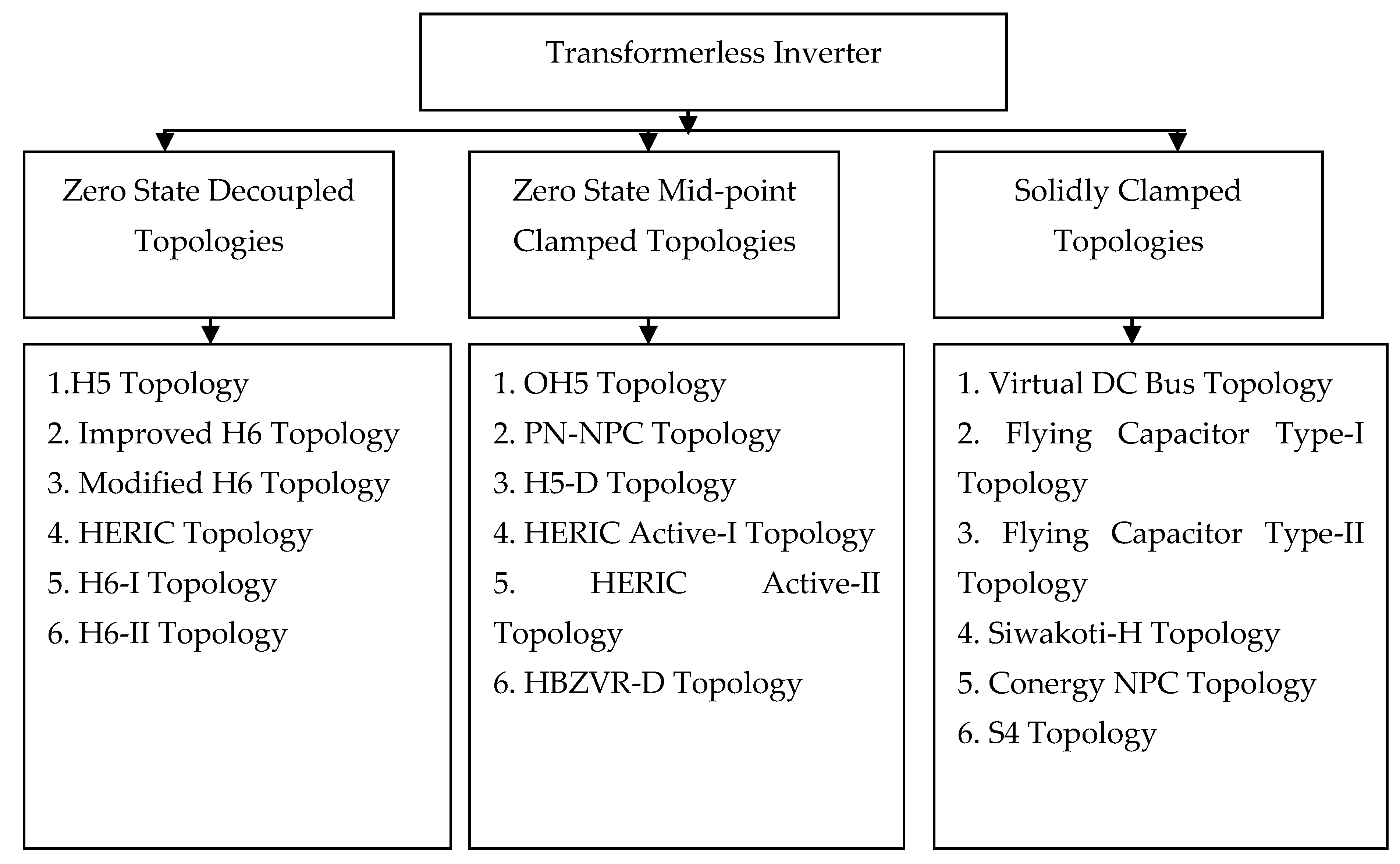
Figure 1.
Classification of selected major single-phase transformerless inverter topologies.
Table 1.
Parameters for simulations and comparisons.
| Parameters | Value |
|---|---|
| AC output voltage | 230 V |
| Line frequency | 50 Hz |
| AC output current | 4.34 A |
| DC input voltage (except Conergy NPC topology) | 400 V |
| DC input voltage (for Conergy NPC topology) | 800 V |
| Output load | 53 Ω |
| Rated power | 998.2 W |
| Switching frequency | 24 kHz |
| DC bus capacitor (Cdc = Cdc1/2 = Cdc2/2) | 940 µF |
| Flying capacitor (CF = C1 = C2) | 1880 µF |
| Filter capacitor (Co) | 0.68 µF |
| Filter inductor (L1 = L2) | 2 mH |
| Parasitic capacitor (CPV = CPV1 = CPV2) | 75 nF |
| Modulation technique | Unipolar SPWM |
2. Zero State Decoupled Topologies
In this category, the best performed six topologies were selected for analysis and comparison purposes. They applied the dc or ac decoupling technique at the zero state to improve the common mode behavior. They are as follows:
2.1. H5 Topology
The H5 topology is shown in Figure 2a. This topology was first proposed in [1]. Using advanced modulation techniques in [2] and the bidirectional clamping approach in [3], the reactive power control of this topology was further enhanced. The switching loss of the H5 topology was reduced using a soft switching strategy in [4] and new modulation techniques in [5]. In terms of filter settings and switching frequency, the H5 topology design was optimized in [6]. Moreover, the full bridge topology was modified to make the structure of this topology. One extra switch, S5, was added for disconnecting the grid from the PV side in the zero state of voltage for the purpose of reducing leakage current. The upper two switches of the full bridge were operated on the line frequency, and the lower two switches on the switching frequency. Figure 2b shows the simulation results of this topology. The advantages of the topology were realized, namely, its higher efficiency, a lower rms value of leakage current, and improved THD in the simulation results. However, the simulation results showed that the peak value of the leakage current was around 200 mA, where the rms value was only 13.23 mA, and the total common mode voltage (VtCM) oscillated from 0 V to 400 V.
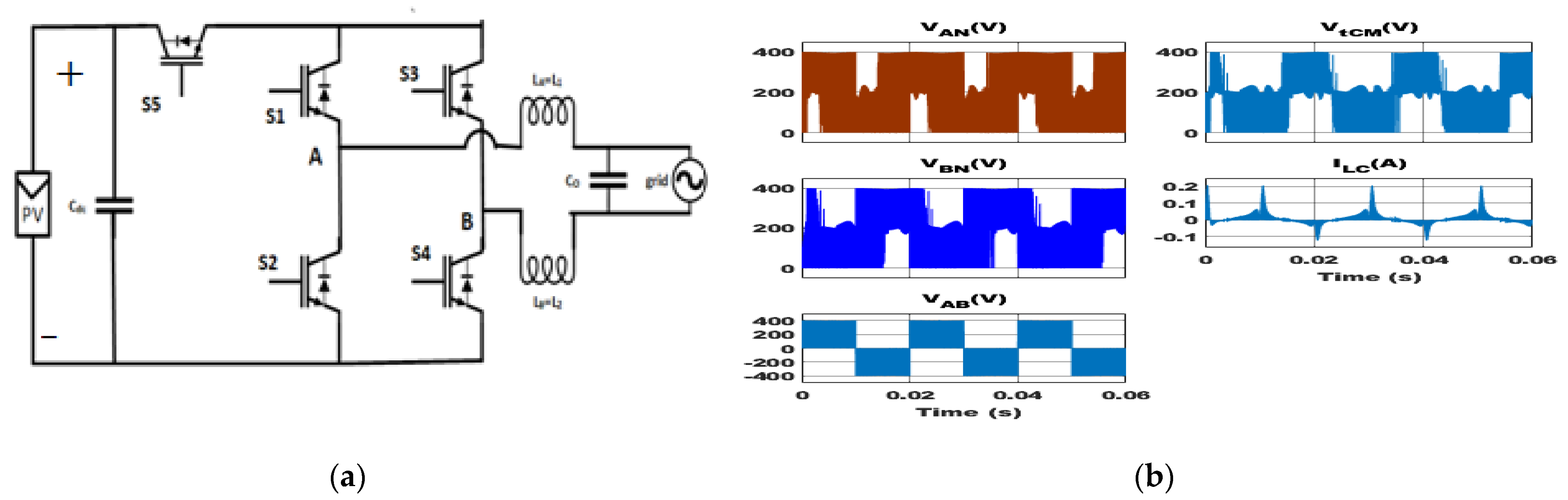
Figure 2.
H5 topology: (
a
) circuit structure; (
b
) simulation results.
2.2. ImprovedH6 Topology
An improved H6 topology was proposed in [7]. In Figure 3a, the topology is shown, and Figure 3b shows the simulation results of this topology. The H5 topology was modified by adding an extra switch in the neutral side of the PV panel to lower the leakage current compared to that of the H5 topology. Here, the left bridge side was operated on the line frequency and right bridge side on the switching frequency. The disconnecting switches were kept on for a half cycle in an alternate manner to avoid more switching loss. The merits of the topology are lower THD and lower leakage current than that of the H5 obtained by simulation. However, the total common mode voltage swung between 0 V and 400 V with a different nature from H5, the peak leakage current was around 150 mA, and the computed efficiency was lower than that of H5 due to the increased number of switches.
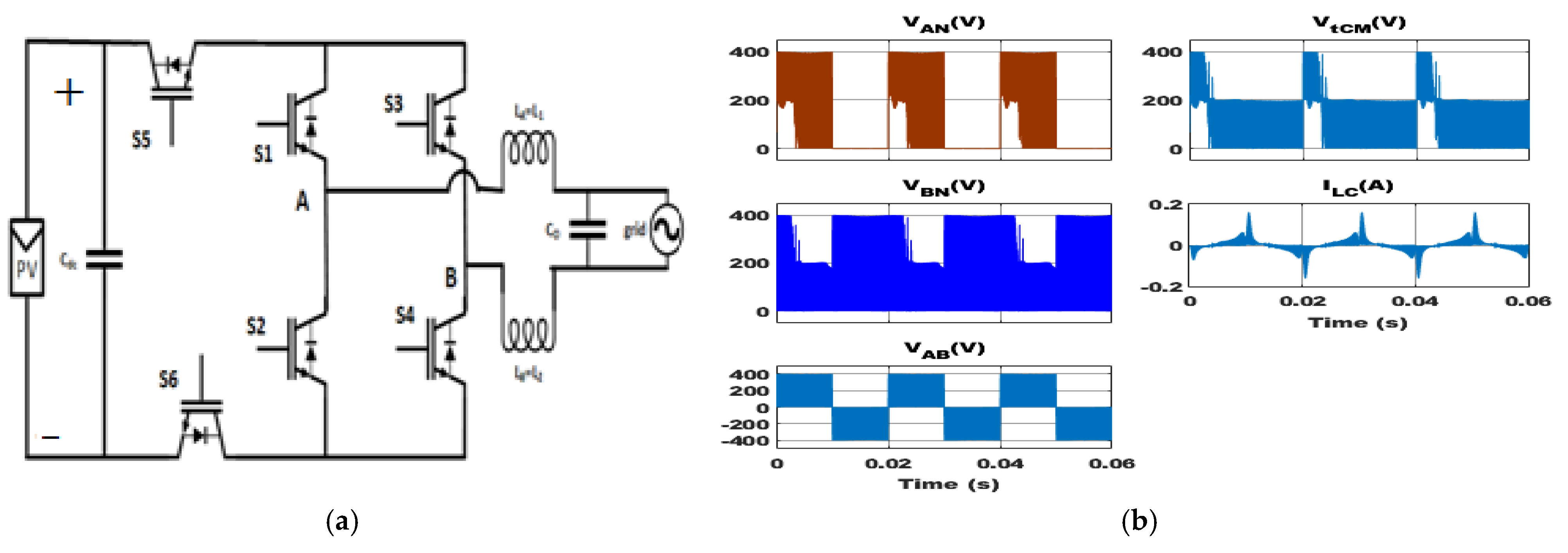
Figure 3.
Improved H6 topology: (
a
) circuit structure; (
b
) simulation results.
2.3. Modified H6 Topology
A modified H6 topology was proposed in [8]. The topology is shown in Figure 4a, and the simulation results of this topology are depicted in Figure 4b. This topology disconnects the PV side from the grid on the free-wheeling mode. The left side of the bridge is operated on the line frequency, and the other four switches are operated on the switching frequency. The nature of the total common mode voltage is evident from the minimal value of leakage current (rms = 12.05 mA, peak = 130 mA), which was somewhat better than that of H5 and the improved H6 topology. The calculated efficiency was higher than the improved H6 but the same as H5. However, in the simulation, the THD was greater than the H5 and the improved H6 topology.
Figure 4.
Modified H6 topology: (
a
) circuit structure; (
b
) simulation results.
2.4. HERIC Topology
The HERIC topology was first proposed in [9]. The topology is drawn in Figure 5a. By utilizing the bidirectional clamping approach in [3] and the advanced modulation technique in [2], this topology’s reactive power capacity was further increased. By using soft switching techniques in [10][11], and enhanced modulation techniques in [12], this topology’s efficiency was raised. Figure 5b displays the simulation results of this topology. Throughout the entire cycle, a portion of the grid current circled through the S5 and S6, progressively reducing the leakage current. By functioning on the line frequency, the S5 and S6 switches serve as ac decoupling switches in the zero and non-zero states. The other four switches are run on the switching frequency. The excellent operation of S5 and S6 makes the topology the most efficient of all decoupling topologies. The simulation results showed the rms leakage current as 12.09 mA, but the peak value was around 125 mA, and the total common mode voltage was also oscillating. The THD of voltage was higher than that of H5 and the improved H6.
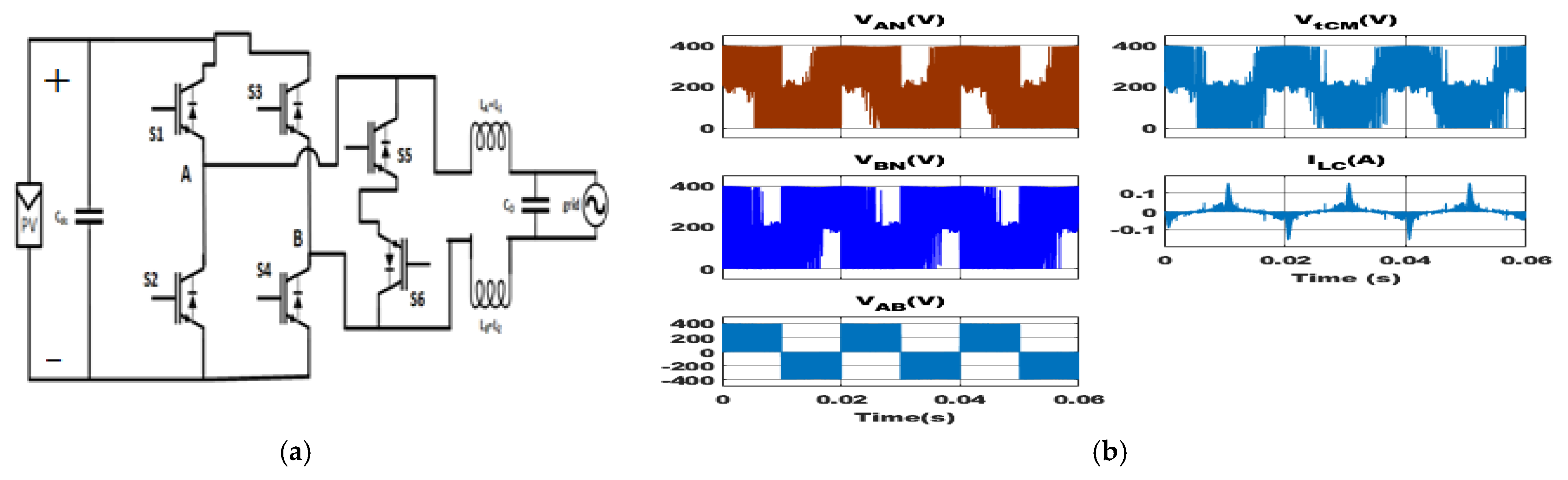
Figure 5.
HERIC topology: (
a
) circuit structure; (
b
) simulation results.
2.5. H6-I Topology
The H6-I topology was primarily proposed in [13]. Figure 6a depicts the topology. Using an advanced hybrid modulation technique, this topology’s capacity to inject reactive power was further improved in [14][15]. By using a new control strategy, the common mode voltage behavior was enhanced in [16]. Figure 116b shows the simulation results of this topology. In this topology, S5 and S6 switches were operated on both active and free-wheeling modes. The diodes were used to flow the free-wheeling current. The other switches were operated on switching frequency. The efficiency of this topology was higher than that of the improved H6 topology due to the lesser switching loss of switches S5 and S6. Its rms leakage current was recorded as 14.94 mA, and the peak was about 150 mA. The THD performance was worse than that of other selected zero state decoupled topologies except for H6-II. This topology’s total common mode voltage oscillated as well.
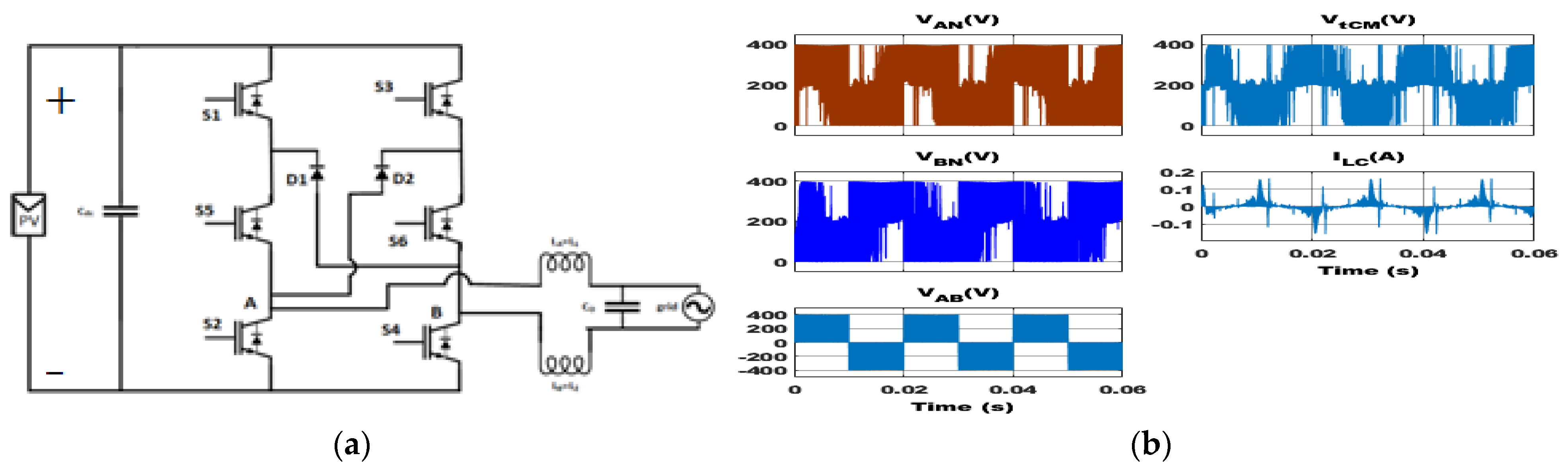
Figure 6.
H6-I topology: (
a
) circuit structure; (
b
) simulation results.
2.6. H6-II Topology
The H6-II topology was firstly proposed in [17]. The topology is sketched in Figure 7a. The reactive power capability was further improved using advanced modulation techniques in [3][18]. Figure 7b shows the simulation results of this topology. S5 and S6 switches were operated in this topology in both active and free-wheeling modes, similar to the H6-I topology. The diodes were used to flow the free-wheeling current. The other switches were operated on the switching frequency. The efficiency of this topology was the same as the H6-I topology due to the same number of switching elements and similar operation principles. The main difference between H6-II and H6-I could be identified from the location of the output terminal of the inverter. Its THD performance and common mode behavior were worse than those of other chosen zero state decoupled topologies.
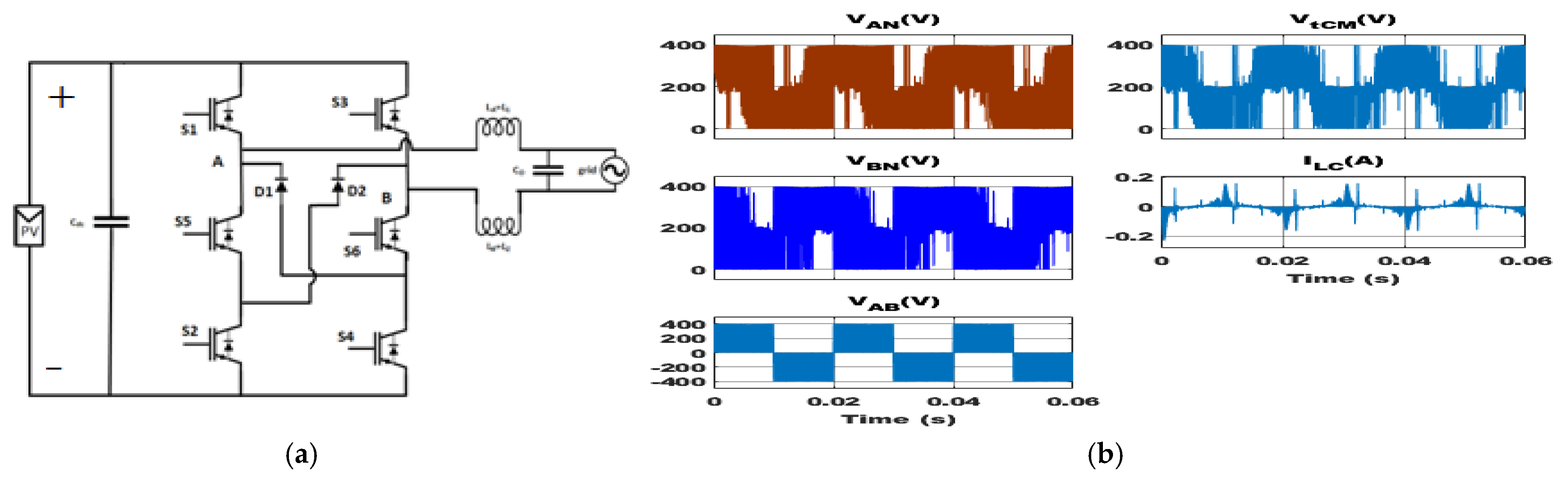
Figure 7.
H6-II topology: (
a
) circuit structure; (
b
) simulation results.
3. Zero State Mid-Point Clamped Topologies
The top six topologies in this category were selected for analysis and comparison. To enhance common mode behavior, they used the mid-point clamping approach at the zero state. They are as follows:
3.1. OH5 Topology
The OH5 topology was proposed in [19]. The topology is shown in Figure 8a, and Figure 8b demonstrates the simulation results of this topology. The upper two switches of the bridge were selected for free-wheeling mode current flowing. The total common mode voltage was now roughly constant at 200 V due to the effective use of switch S6 in the zero state or free-wheeling mode. However, because both the inductor and the capacitor impact leakage current, when the first half of the cycle was ignored, simulation results showed a continuous leakage current of 65.05 mA without a peak. However, this topology’s efficiency was the lowest among those in this category due to the running of more switches at the switching frequency.
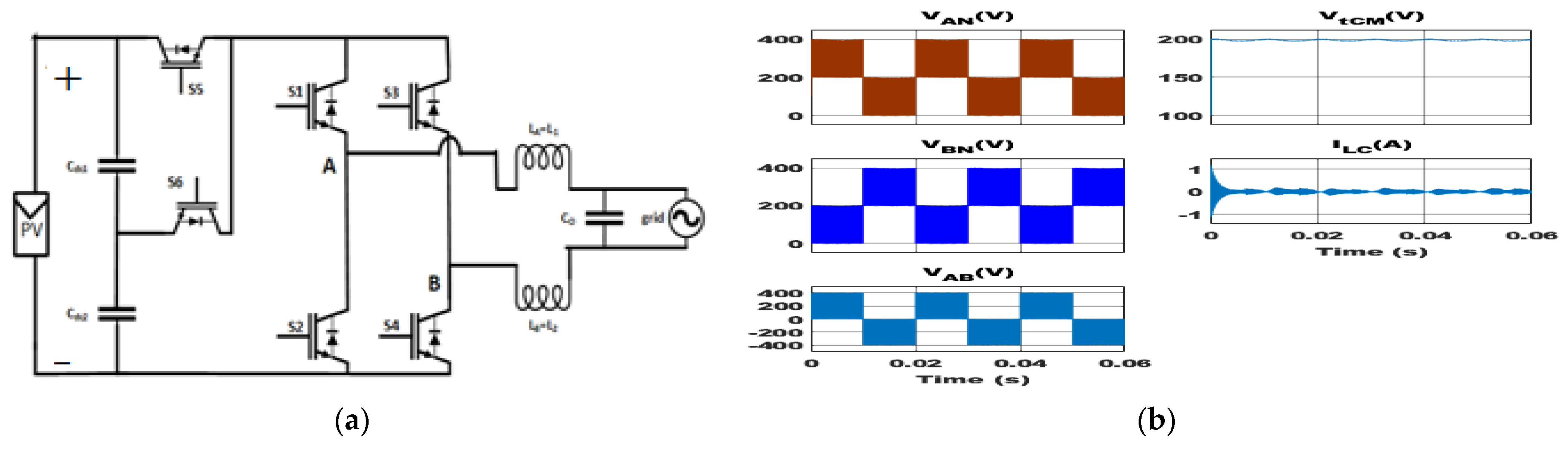
Figure 8.
OH5 topology: (
a
) circuit structure; (
b
) simulation results.
3.2. PN-NPC Topology
The PN-NPC topology was proposed in [20]. Figure 9a depicts a topology drawing, and Figure 9b displays simulation results of this topology. Eight switches were utilized in this topology, four of which were operated on line frequency and the remaining four on the switching frequency. Switches S7 and S8 were selected for the clamping function on the zero state as well as on the active state. When compared to the other zero state mid-point clamping topologies, its THD performance was ranked second. The standard efficiency was maintained by running the four switches on the line frequency. Although only 13.29 mA rms value of leakage current was present, simulation results showed a 100 mA spike at an incorrect clamping point.
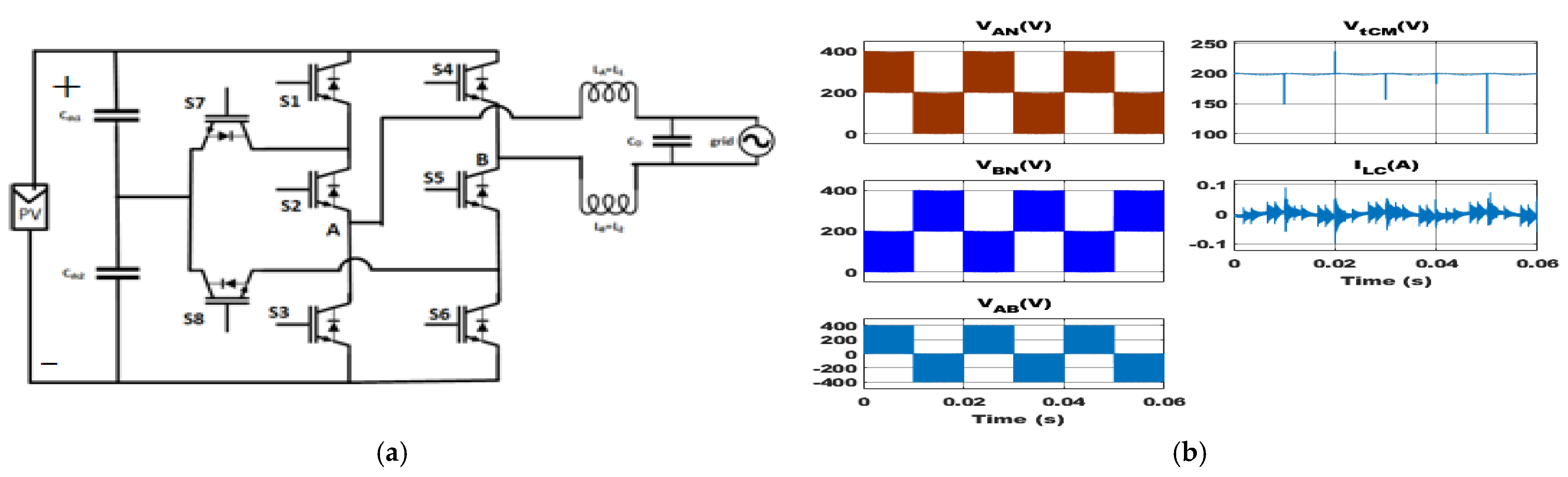
Figure 9.
PN-NPC topology: (
a
) circuit structure; (
b
) simulation results.
3.3. H5-D Topology
The H5-D topology was proposed in [21]. The topology is shown in Figure 10a. Figure 10b shows the simulation results of this topology. In this topology, diode D1 was used for clamping purposes. Switches S2 and S4 were turned on during the free-wheeling mode. Despite not obtaining a single stable common mode voltage, the swing was restricted to 0 V to 200 V. The rms leakage current was 13.88 mA, although simulations showed 100 mA peaks due to incorrect clamping. However, the THD performance was the best among the chosen zero state mid-point clamping topologies. The estimated efficiency was higher than OH5 at 97.3%.
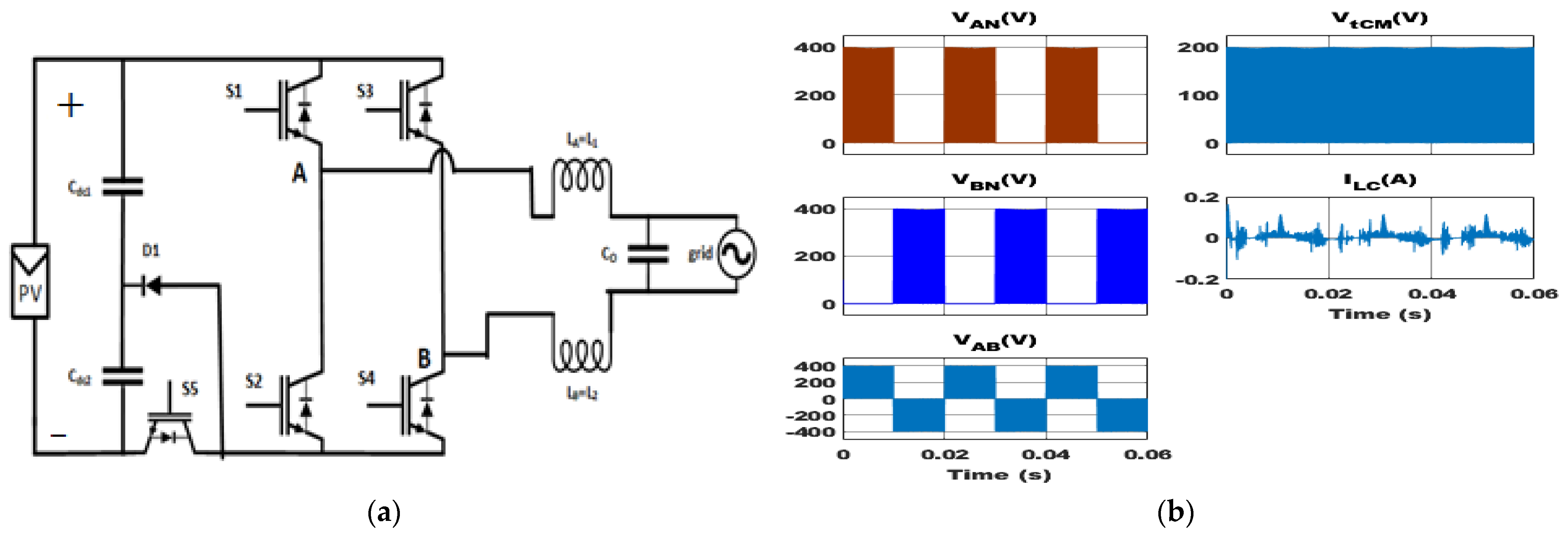
Figure 10.
H5-D topology: (
a
) circuit structure; (
b
) simulation results.
3.4. HERIC Active-I Topology
The HERIC Active-I topology was proposed in [22]. Figure 11a sketches out the topology, and Figure 11b shows the simulation results of this topology. Switch S7 solely clamped the midpoint voltage in the positive half cycle’s zero state. S5 and S6 were operated on the line frequency to create an extra free-wheeling path using the ac decoupling technique. The efficiency of this topology was the highest among the selected topologies under this category due to lower conduction losses. The rms leakage current was 41.41 mA, and the peak value was about 120 mA. Because only the positive half cycle was clamped, there was a relatively higher leakage current.
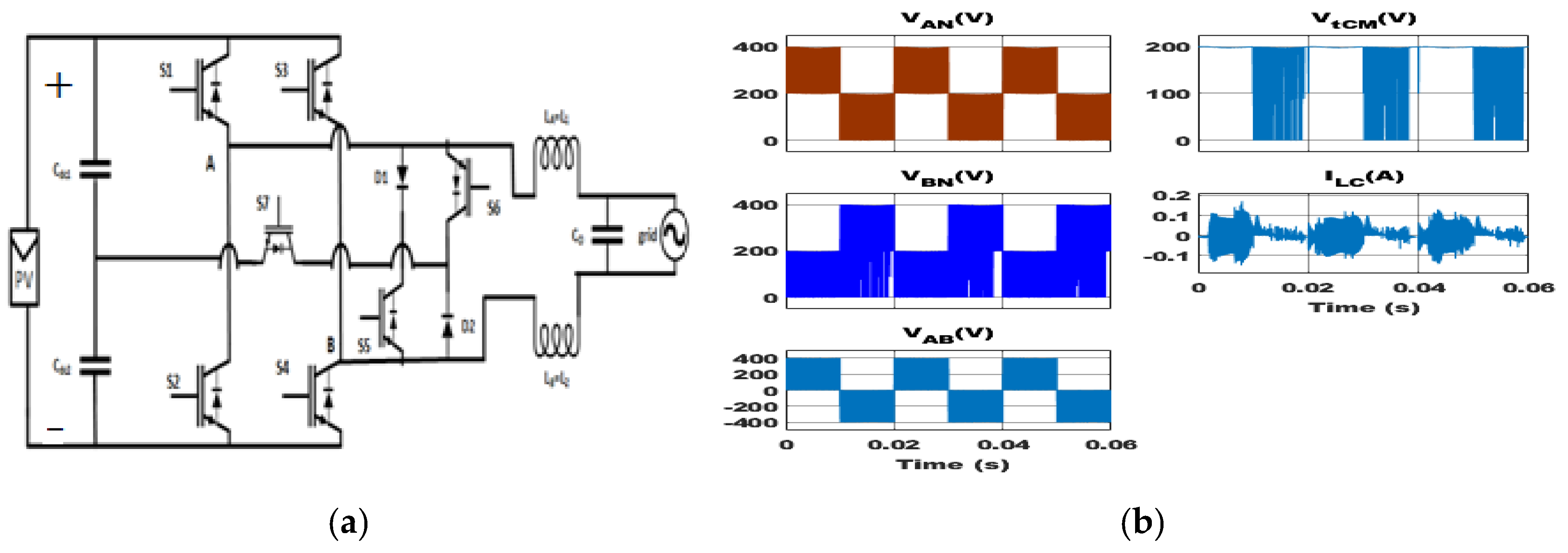
Figure 11.
HERIC Active-I topology: (
a
) circuit structure; (
b
) simulation results.
3.5. HERIC Active-II Topology
The HERIC Active-II topology was proposed in [22]. The topology is shown in Figure 12a, and the simulation results of this topology are depicted in Figure 12b. Switch S7 was used for clamping purposes, and it was operated on the switching frequency on the zero voltage state. For the purpose of ac decoupling, switches S5 and S6 were operated at the line frequency. The efficiency of this topology was higher than that of H5-D and PN-NPC topologies. The leakage current’s peak value was restricted to 100 mA, despite the fact that the leakage current rms value was somewhat greater than that of other chosen topologies in this category.
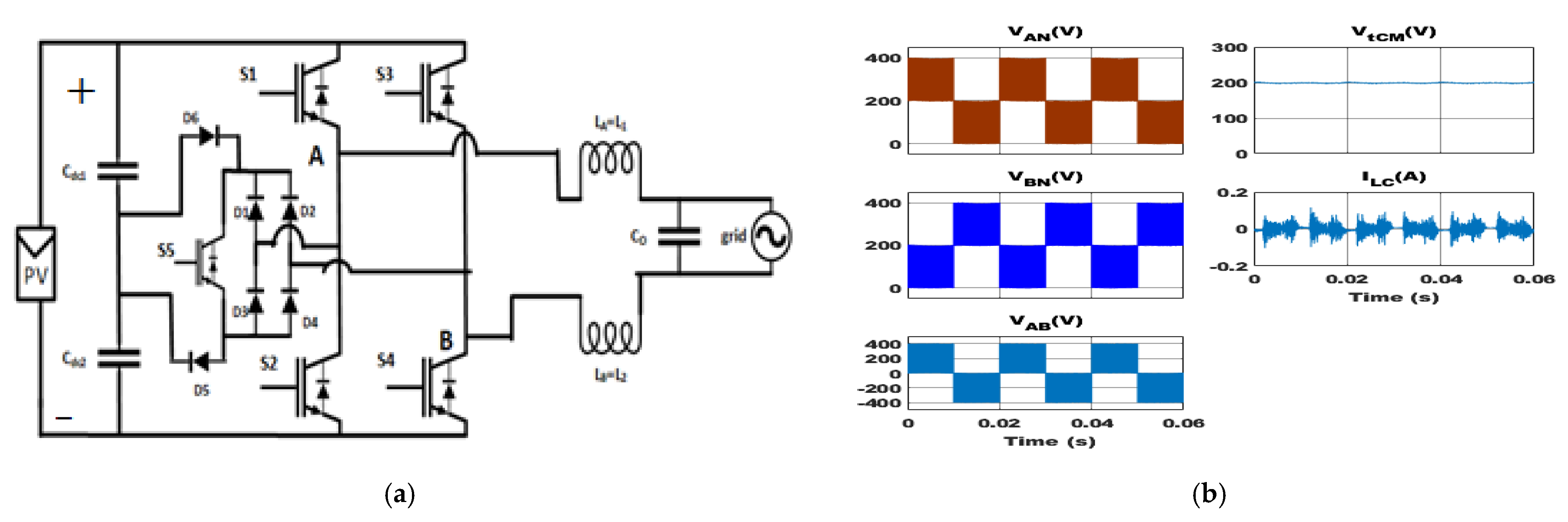
Figure 12.
HERIC Active-II topology: (
a
) circuit structure; (
b
) simulation results.
3.6. HBZVR-D Topology
The HBZVR-D topology was proposed in [23]. Figure 13a shows a drawing of the topology, and Figure 13b shows the simulation results of this topology. Two diodes, D5 and D6, were employed for clamping the mid-point voltage. Switch S5 was used for creating the free-wheeling path during the zero state. The free-wheeling path was made possible by the anti-parallel diodes D1–D4. The rms leakage current was 22.75 mA, and the total common mode voltage was about a constant 200 V. This topology’s computed efficiency was 97.6%, which was higher than that of the OH5 and H5-D topologies. However, the leakage current’s peak value was about 110 mA.

Figure 13.
HBZVR-D topology: (
a
) circuit structure; (
b
) simulation results.
4. Solidly Clamped Topologies
In this category, the most optimum six topologies were selected for analysis and comparison purposes. They used a solid connection from the grid negative terminal to either the PV neutral or the mid-point of two series dc link capacitors to improve the common mode behavior. They are as follows:
4.1. Virtual DC Bus Topology
The Virtual DC Bus topology was proposed in [24]. The topology is shown in Figure 14a, and the simulation results of this topology are sketched in Figure 14b. The capacitor C2 was charged during the positive half cycle to create a virtual DC bus for the negative half cycle. The S3 and S5 switches were activated during the positive half cycle free-wheeling mode, while the S2 and S4 switches were activated during the negative half cycle free-wheeling mode. This topology’s total common mode voltage was about 0 V because the grid’s negative terminal was directly connected to the PV side’s neutral. The rms leakage current was only 0.75 mA, but the leakage current peak value was roughly 7.5 mA. The efficiency was only 96.8% due to high conduction losses.
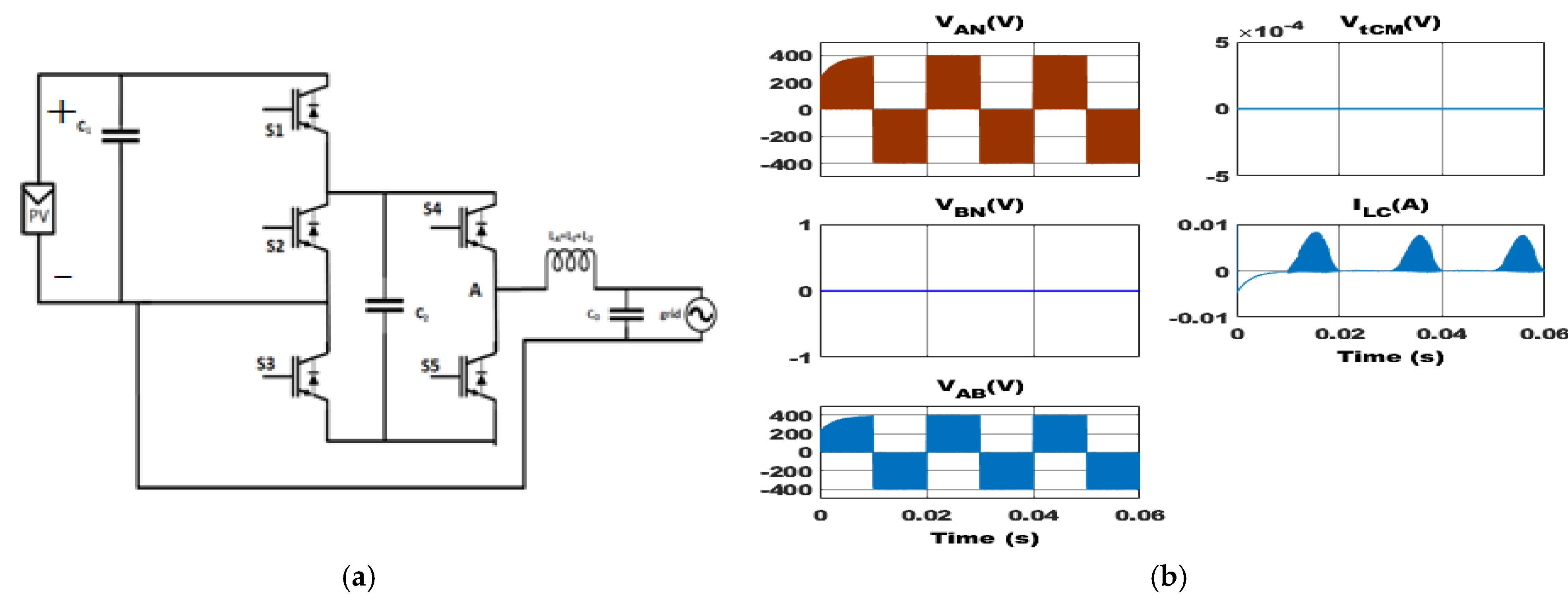
Figure 14.
Virtual DC Bus topology: (
a
) circuit structure; (
b
) simulation results.
4.2. Flying Capacitor Type-I tTopology
The Flying Capacitor Type-I topology was proposed in [25]. Figure 15a shows a sketch of the topology, and Figure 15b shows the simulation results of this topology. The flying capacitor CF was charged during the whole positive half cycle, and it acted as the source for the negative half cycle through discharging. Although all switches functioned at the switching frequency, because the length was only half a cycle, switching loss was cut in half. Although capacitor charging caused additional conduction loss, the efficiency was still quite high at 97.2%. Since it is evident from the simulation that the total common mode voltage was set at zero volts, the rms leakage current was only 0.58 mA. However, starting the leakage current’s peak value at 8.5 mA, it decreased over time. Furthermore, the output voltage’s THD was 4.2%.
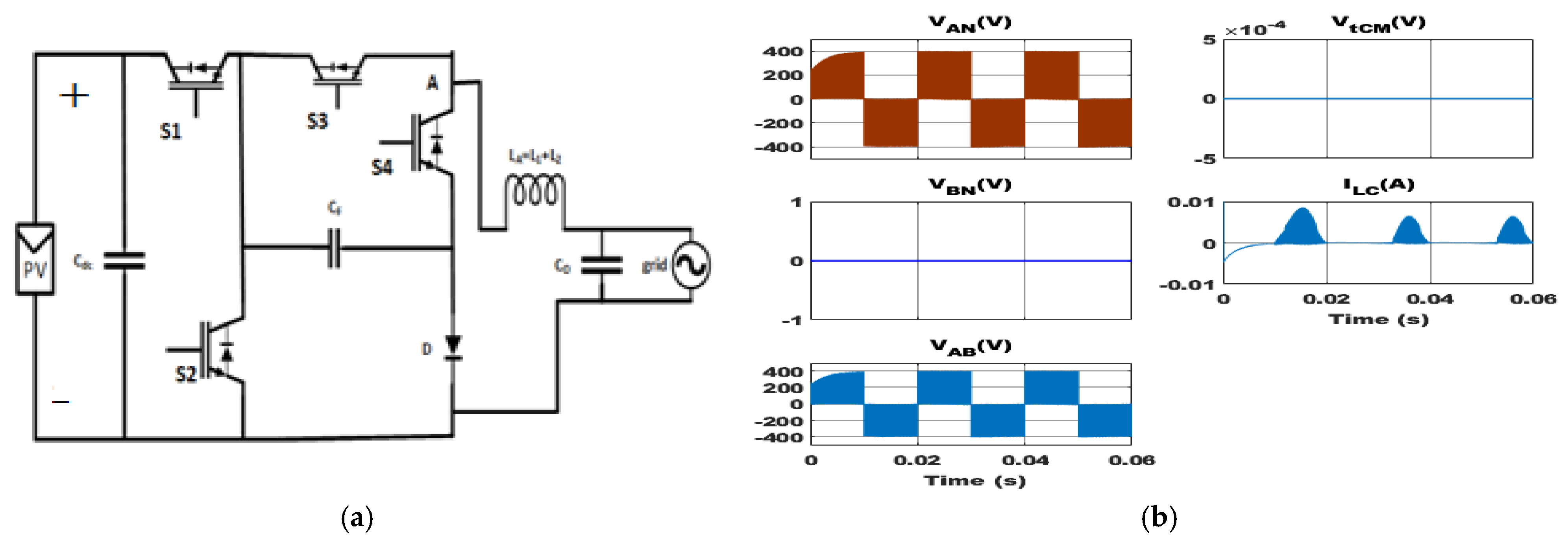
Figure 15.
Flying Capacitor Type-I topology: (
a
) circuit structure; (
b
) simulation results.
4.3. Flying Capacitor Type-II Topology
The Flying Capacitor Type-II topology was proposed in [26]. The topology is drawn in Figure 16a, and the simulation results of this topology are shown in Figure 16b. Throughout the entirety of the positive half cycle, the flying capacitor CF was charged through switch S1 and diode D. The grid was powered by the charged capacitor CF during the negative half cycle. To lower the switching loss, switches S1 and S4 were activated during the free-wheeling mode for a half-cycle period on the line frequency and another half-cycle on the switching frequency. The total common mode voltage was confirmed by simulation results to be 0 V, and as a result, the rms leakage current was just 0.58 mA. Although the leakage current’s peak value starting from 8 mA diminishes with time. The obtained efficiency of this topology was the same as that of the Flying Capacitor Type-I topology at 97.2%, and the voltage THD was 4.2%.
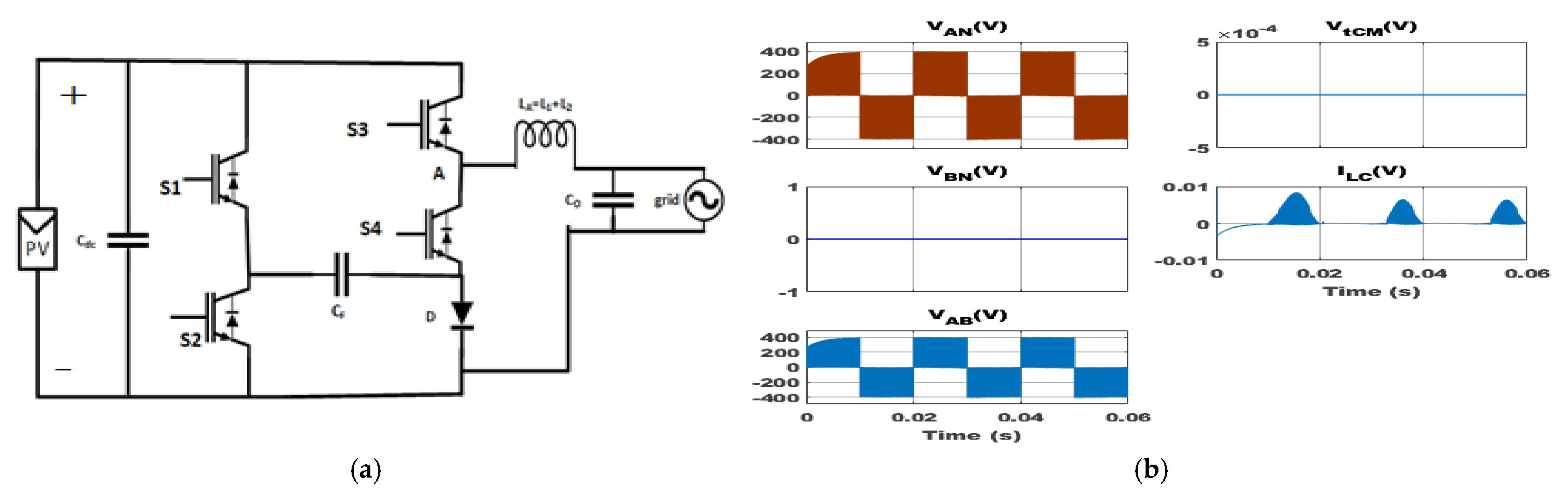
Figure 16.
Flying Capacitor Type-II topology: (
a
) circuit structure; (
b
) simulation results.
4.4. Siwakoti-H Topology
The Siwakoti-H topology was first proposed in [27]. The topology is represented in Figure 17a. The nonlinear behavior of this topology was properly addressed using a discrete-time state feedback control scheme in [28], and using a direct model predictive control scheme in [29]. Figure 17b shows the simulation results of this topology. Two switches called S1 and S4 were reverse blocking IGBT (RB-IGBT), and they were operated on the zero state to charge the flying capacitor CF. This fully charged capacitor was used as the source of the negative active half cycle. The positive active half cycle was controlled by switch S3. The total common mode voltage was observed as 0 V from the simulation, and hence the rms leakage current value was only 0.47 mA. However, the 40 mA leakage current peak was seen in the first cycle. The computed efficiency was second in this category at 98.1%, and the simulation showed a voltage THD of 4.3%.
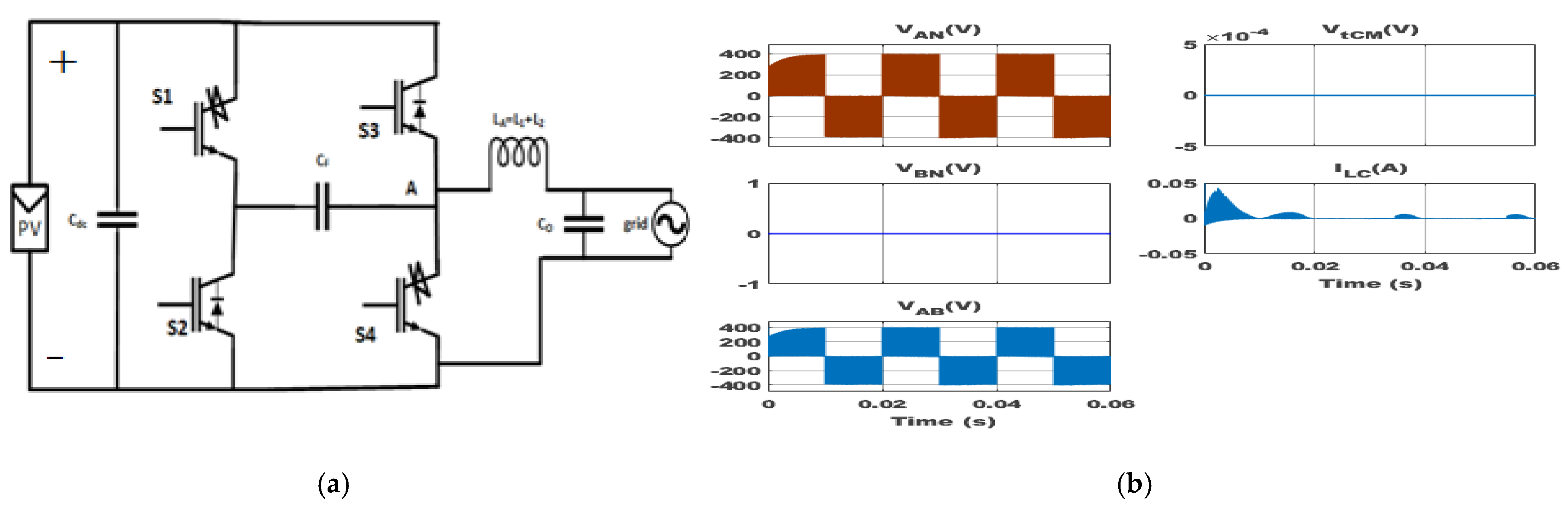
Figure 17.
Siwakoti-H topology: (
a
) circuit structure; (
b
) simulation results.
4.5. Conergy NPC Topology
The Conergy NPC topology was primarily proposed in [30]. The topology is redrawn in Figure 18a. According to switching frequency and filter parameters, this topology with SiC switches was designed optimally in [6]. Figure 18b shows the simulation results of this topology. The negative terminal of the grid was directly attached to the middle point of two equal-series dc link capacitors. To flow the current in the free-wheeling mode, switches S3 and S4 were operated in the zero state in the opposite way. Although the total common mode voltage was about 400 V, nevertheless, the leakage current rms value was limited to 0.14 mA with no noticeable peaks due to its solid connection and constant VtCM. Due to its extremely low conduction loss, this topology had the highest efficiency among those in this category. The voltage THD was also 1%. However, the input voltage requirement of this topology was twice than that of other topologies.
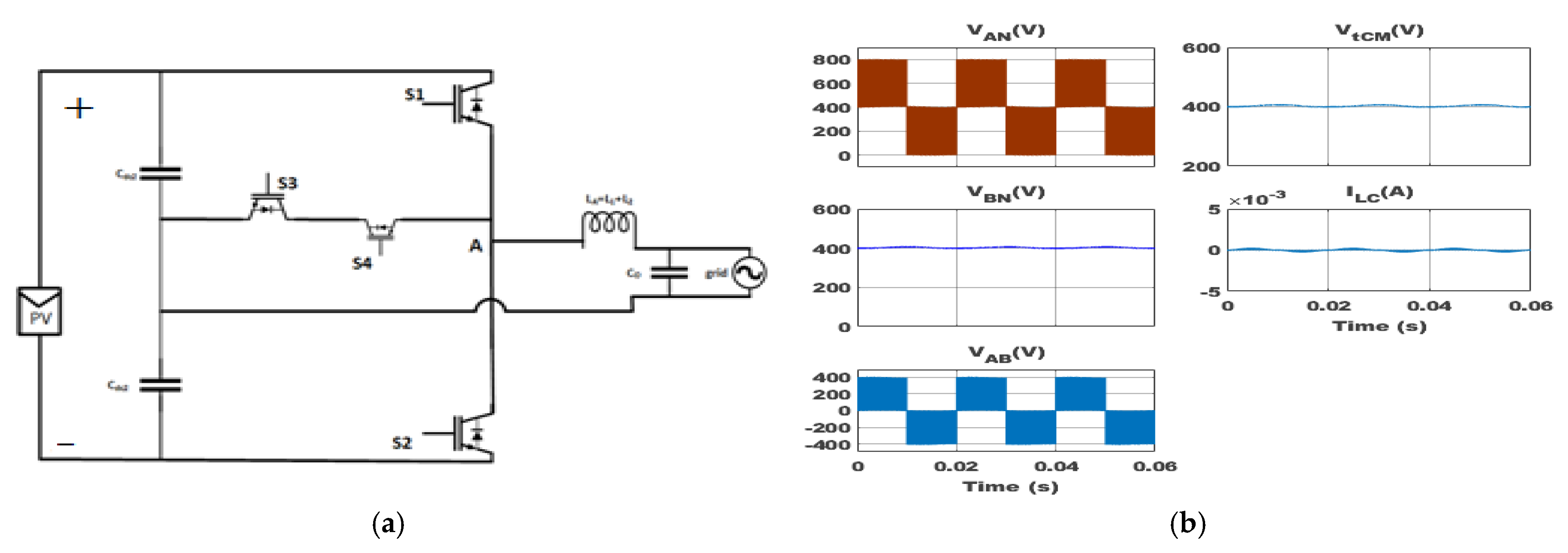
Figure 18.
Conergy NPC topology: (
a
) circuit structure; (
b
) simulation results.
4.6. S4 Topology
The S4 topology was proposed in [31]. Figure 19a depicts the topology, and the simulation results of this topology are depicted in Figure 19b. In the positive half cycle active mode, C1 charged through diode D2, and then C2 charged from the discharge of C1 through D1 in the positive zero state. In the negative half cycle, C2 provided power to the grid. The total common mode voltage was 0 V, and hence the rms leakage current was only 0.56 mA. Because switching frequency was used the majority of the time to run all switches, efficiency was impacted, and the computed efficiency was only 96.2%. Furthermore, compared to other chosen topologies, the voltage THD was worse.
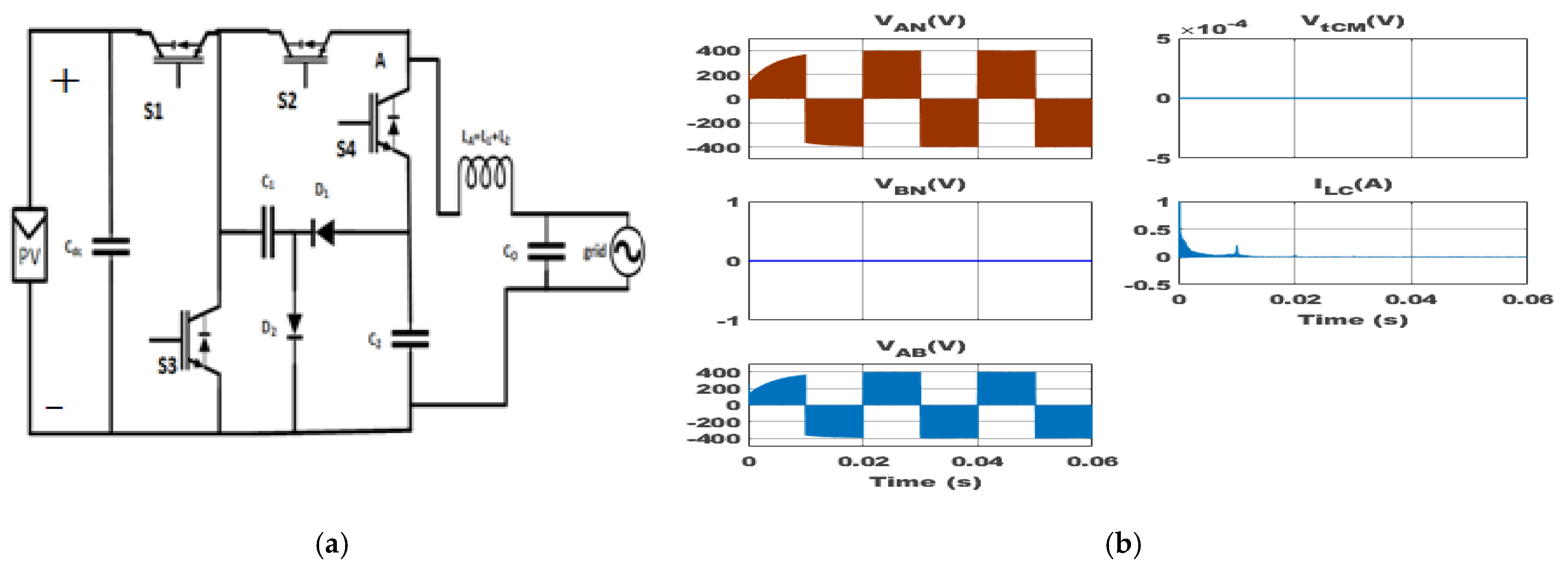
Figure 19.
S4 topology: (
a
) circuit structure; (
b) simulation results.
) simulation results.
References
- Victor, M.; Greizer, F.; Bremicker, S.; Hübler, U. Method of Converting a Direct Current Voltage from a Source of Direct Current Voltage, More Specifically from a Photovoltaic Source of Direct Current Voltage, into a Alternating Current Voltage. U.S. Patent 411802B2, 12 August 2008.
- Freddy, T.K.S.; Lee, J.H.; Moon, H.C.; Lee, K.B.; Rahim, N.A. Modulation Technique for Single-Phase Transformerless Photovoltaic Inverters with Reactive Power Capability. IEEE Trans. Ind. Electron. 2017, 64, 6989–6999.
- Kumar, K.S.; Kirubakaran, A.; Subrahmanyam, N. Bidirectional Clamping-Based H5, HERIC, and H6 Transformerless Inverter Topologies with Reactive Power Capability. IEEE Trans. Ind. Appl. 2020, 56, 5119–5128.
- Fang, J.; Shi, M.; Xiao, H.; Wang, R. A Zero-Voltage-Transition H5-Type Transformerless Photovoltaic Grid-Connected Inverter. IEEE Access 2019.
- Mahfuz-Ur-Rahman, A.M.; Islam, M.R.; Muttaqi, K.M.; Rahman, M.A.; Sutanto, D. An Advanced Modulation Technique for Transformer-Less Grid-Connected Inverter Circuits Used in Solar Photovoltaic Systems. IEEE Trans. Ind. Electron. 2022, 70, 3878–3887.
- Saridakis, S.; Koutroulis, E.; Blaabjerg, F. Optimization of SiC-Based H5 and Conergy-NPC Transformerless PV Inverters. IEEE J. Emerg. Sel. Top. Power Electron. 2015, 3, 555–567.
- Yang, B.; Li, W.; Gu, Y.; Cui, W.; He, X. Improved Transformerless Inverter with Common-Mode Leakage Current Elimination for a Photovoltaic Grid-Connected Power System. IEEE Trans. Power Electron. 2012, 27, 752–762.
- Rahman, M.M.; Hossain, M.S.; Talukder, M.S.I.; Uddin, M.N. Transformerless Six-Switch (H6)-Based Single-Phase Inverter for Grid-Connected Photovoltaic System with Reduced Leakage Current. IEEE Trans. Ind. Appl. 2022, 58, 974–985.
- Schmidt, H.; Siedle, C.; Ketterer, J. DC/AC Converter to Convert Direct Electric Voltage into Alternating Voltage or into Alternating Current. U.S. Patent 7 046 534, 16 May 2006.
- Xiao, H.; Zhang, L.; Wang, Z.; Cheng, M. A New Soft-Switching Configuration and Its Application in Transformerless Photovoltaic Grid-Connected Inverters. IEEE Trans. Ind. Electron. 2018, 65, 9518–9527.
- Xiao, H.F.; Zhang, L.; Li, Y. A Zero-Voltage-Transition HERIC-Type Transformerless Photovoltaic Grid-Connected Inverter. IEEE Trans. Ind. Electron. 2017, 64, 1222–1232.
- Tang, Z.; Su, M.; Sun, Y.; Cheng, B.; Yang, Y.; Blaabjerg, F.; Wang, L. Hybrid UP-PWM Scheme for HERIC Inverter to Improve Power Quality and Efficiency. IEEE Trans. Power Electron. 2019, 34, 4292–4303.
- Ji, B.; Wang, J.; Zhao, J. High-Efficiency Single-Phase Transformerless PV H6 Inverter with Hybrid Modulation Method. IEEE Trans. Ind. Electron. 2013, 60, 2104–2115.
- Wang, J.; Luo, F.; Ji, Z.; Sun, Y.; Ji, B.; Gu, W.; Zhao, J. An Improved Hybrid Modulation Method for the Single-Phase H6 Inverter with Reactive Power Compensation. IEEE Trans. Power Electron. 2018, 33, 7674–7683.
- Wang, J.; Gao, S.; Sun, Y.; Ji, Z.; Cheng, L.; Li, L.; Gu, W.; Zhao, J. Single Phase Bidirectional H6 Rectifier/Inverter. IEEE Trans. Power Electron. 2019, 34, 10710–10719.
- Yang, Y.; Yang, Y.; He, L.; Fan, M.; Xiao, Y.; Chen, R.; Xie, M.; Zhang, X.; Zhang, L.; Rodriguez, J. A Novel Cascaded Repetitive Controller of an LC-Filtered H6 Voltage-Source Inverter. IEEE J. Emerg. Sel. Top. Power Electron. 2022.
- Yu, W.; Lai, J.S.; Qian, H.; Hutchens, C. High-Efficiency MOSFET Inverter with H6-Type Configuration for Photovoltaic Nonisolated AC-Module Applications. IEEE Trans. Power Electron. 2011, 26, 1253–1260.
- Liu, B.; Su, M.; Yang, J.; Song, D.; He, D.; Song, S. Combined Reactive Power Injection Modulation and Grid Current Distortion Improvement Approach for H6 Transformer-Less Photovoltaic Inverter. IEEE Trans. Energy Convers. 2017, 32, 1456–1467.
- Xiao, H.; Xie, S.; Chen, Y.; Huang, R. An Optimized Transformerless Photovoltaic Grid-Connected Inverter. IEEE Trans. Ind. Electron. 2011, 58, 1887–1895.
- Zhang, L.; Sun, K.; Feng, L.; Wu, H.; Xing, Y. A Family of Neutral Point Clamped Full-Bridge Topologies for Transformerless Photovoltaic Grid-Tied Inverters. IEEE Trans. Power Electron. 2013, 28, 730–739.
- Li, H.; Zeng, Y.; Zhang, B.; Zheng, T.Q.; Hao, R.; Yang, Z. An Improved H5 Topology with Low Common-Mode Current for Transformerless PV Grid-Connected Inverter. IEEE Trans. Power Electron. 2019, 34, 1254–1265.
- Li, W.; Gu, Y.; Luo, H.; Cui, W.; He, X.; Xia, C. Topology Review and Derivation Methodology of Single-Phase Transformerless Photovoltaic Inverters for Leakage Current Suppression. IEEE Trans. Ind. Electron. 2015, 62, 4537–4551.
- Freddy, T.K.S.; Rahim, N.; Hew, W.-P.; Che, H.S. Comparison and Analysis of Single-Phase Transformerless Grid-Connected PV Inverters. IEEE Trans. Power Electron. 2014, 29, 5358–5369.
- Gu, Y.; Li, W.; Zhao, Y.; Yang, B.; Li, C.; He, X. Transformerless Inverter with Virtual DC Bus Concept for Cost-Effective Grid-Connected PV Power Systems. IEEE Trans. Power Electron. 2013, 28, 793–805.
- Siwakoti, Y.P.; Blaabjerg, F. A Novel Flying Capacitor Transformerless Inverter for Single-Phase Grid Connected Solar Photovoltaic System. In Proceedings of the 2016 IEEE 7th International Symposium on Power Electronics for Distributed Generation Systems (PEDG), Vancouver, BC, Canada, 27–30 June 2016.
- Siwakoti, Y.P.; Blaabjerg, F. Common-Ground-Type Transformerless Inverters for Single-Phase Solar Photovoltaic Systems. IEEE Trans. Ind. Electron. 2018, 65, 2100–2111.
- Siwakoti, Y.P.; Blaabjerg, F. H-Bridge Transformerless Inverter with Common Ground for Single-Phase Solar-Photovoltaic System. In Proceedings of the 2017 IEEE Applied Power Electronics Conference and Exposition (APEC), Tampa, FL, USA, 26–30 March 2017; pp. 2610–2614.
- Begh, M.A.W.; Liegmann, E.; Mahajan, A.; Palanisamy, A.; Siwakoti, Y.P.; Karamanakos, P.; Abdelrahem, M.; Kennel, R. Design of State-Feedback Controller for a Single-Phase Grid-Connected Siwakoti-h Inverter with LCL Filter. In Proceedings of the PCIM Europe Conference 2019, Nuremberg, Germany, 7–9 May 2019; pp. 1587–1594.
- Begh, M.A.W.; Liegmann, E.; Karamanakos, P.; Kennel, R. Direct Model Predictive Control of a Single-Phase Grid-Connected Siwakoti-H Inverter. In Proceedings of the IECON (The 46th Annual Conference of the Industrial Electronics Conference), Singapore, 18–21 October 2020; Volume 2020, pp. 3045–3050.
- Knaup, P. International Patent Application. WO Patent 048 420 A1, 3 May 2007.
- Ardashir, J.F.; Sabahi, M.; Hosseini, S.H.; Blaabjerg, F.; Babaei, E.; Gharehpetian, G.B. A Single-Phase Transformerless Inverter with Charge Pump Circuit Concept for Grid-Tied PV Applications. IEEE Trans. Ind. Electron. 2017, 64, 5403–5415.
More