Your browser does not fully support modern features. Please upgrade for a smoother experience.
Please note this is a comparison between Version 1 by Jacek Wojtas and Version 2 by Camila Xu.
Photodetectors are one of the popular types of technology used in ultraviolet radiation research. They are widely used in the industrial area (flame detectors, fire alarm systems, extreme UV lithography), national security (missile defense, military recognition, explosives detection, forensic analysis, secure communications), in fields such as medicine (UV imaging, protein analysis, and DNA sequencing) or biology (biological agent detection), and when dealing with environmental issues (ozone detection, air pollution determination, disinfection, and decontamination).
- ultraviolet photodetectors
- photoemissive UV photodetectors
- silicon-based UV detectors
1. Introduction
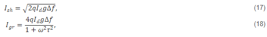
Ultraviolet (UV) radiation is an important component of solar radiation (Figure 1a), which has a significant impact on the development and survival of mankind. Extreme UV radiation can cause various diseases, including cataracts and skin cancer, and accelerate the aging process. This radiation also has a significant impact on crop yields and the vitality of infrastructure. Recent studies have shown that a 1% reduction in the thickness of the ozone layer will increase UV radiation near the earth’s surface by 2%, resulting in a 3% increase in melanoma incidence [1][2][1,2]. Accordingly, the search for UV photodetection has attracted the interest of scientists in related fields. The International Commission on Non-Ionizing Radiation Protection regulates UV radiation limits for humans, as shown in Figure 1b.
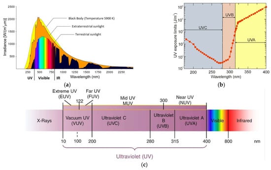
Figure 1. Solar irradiation spectrum: (a) threes spectra [the spectrum of a black body with a temperature of 5900 K similar to the solar spectrum, the actual spectrum of the sun at the outer edge of the earth’s atmosphere (extra-terrestrial solar radiation), and the spectrum at sea level (terrestrial solar radiation), (b) human exposure limits as a function of wavelength in the UV spectrum, and (c) the UV spectral region and its subdivisions.
Photodetectors are one of the popular types of technology used in ultraviolet radiation research. They are widely used in the industrial area (flame detectors, fire alarm systems, extreme UV lithography), national security (missile defense, military recognition, explosives detection, forensic analysis, secure communications), in fields such as medicine (UV imaging, protein analysis, and DNA sequencing) or biology (biological agent detection), and when dealing with environmental issues (ozone detection, air pollution determination, disinfection, and decontamination).
Ultraviolet radiation is electromagnetic radiation from 10 nm to 400 nm (Figure 1c). It is shorter than radiation in the visible spectrum but longer than X-rays. The ultraviolet spectrum is also subdivided due to each band’s effect on the biosphere [3]:
-
UV-A—wavelengths: 315–400 nm;
-
UV-B—wavelengths: 280–315 nm;
-
UV-C—wavelengths: 100–280 nm.
The sun emits the entire range of UV radiation; therefore, the radiation of the UV-A range and part of the UV-B radiation range reaches the Earth’s surface (Figure 2). The ozone (triatomic oxygen) layer absorbs most of the UV-B, while the diatomic oxygen in the atmosphere absorbs all radiation below 200 nm [4].
Figure 2.
Blocking different bands of UV radiation.
UV radiation detection systems use photographic films (nowadays very rarely), thermal, and photon detectors. Historically, the first image-capturing method is one of the oldest and most efficient in the UV range for wavelengths above 200 nm, where gelatine shows noticeable absorption [5]. A single exposure allows for the capture of large amounts of data on photographic films. However, they have serious disadvantages: their sensitivity is lower than that of photon detectors, their responsivity has a non-linear dependence on the incident photon flux at a given wavelength, and their spectral response is broad.
On the other hand, the sensitivity of thermal detectors is much lower than that of photon detectors. They are absolute radiometric standards in the ultraviolet range of the spectrum. Photon detectors based on external or internal photoelectric phenomena overcome the abovementioned limitations and offer superior performance. The main objective is to develop surveillance imaging systems for military and civilian applications with the following criteria:
-
Not light-sensitive (solar blind);
-
High quantum efficiency;
The photodiodes become a more significant type of detector over time. They have many advantages, such as low power dissipation, inherently high impedance, and negligible 1/f noise. Due to the fact that they can be easily multiplexed using the ROIC, the number of pixels in two-dimensional (2D) arrays is limited by existing technologies. Due to the higher doping levels in the absorber of the photodiode and the fast collection of the carriers, the photodiode output signal remains linear for substantially higher photon flux compared to photoconductors.
Table 1.
List of different types of photon detectors with their brief characterization.
| Type of Detector | Detector Structure | Diagram of Energy Band |
|---|---|---|
| Photoemissive detector | ||
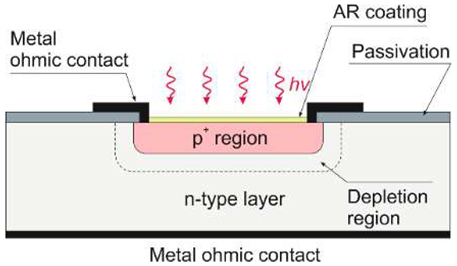
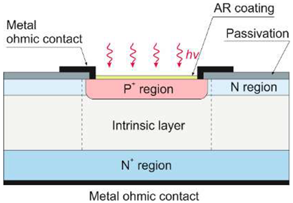
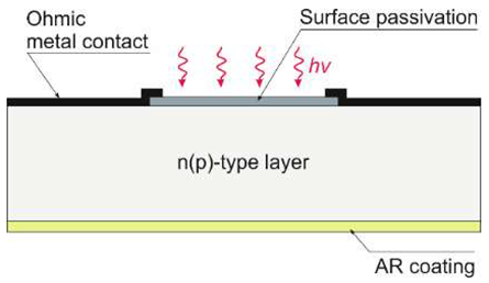
| P–N junction photodiode This is a widely used photodetector in a typical p-on-n configuration with a shallowly diffused p-region on the n-type active layer. An n-on-p structure is also available. An electric field separates photo-created electron-hole pairs on either side of the junction in the space charge region. The generated photocurrent changes the open-circuit junction voltage or the short-circuit junction current. |
 |
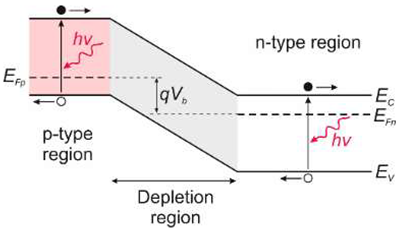 |
| P-i-N photodiode P-i-N is merely a standard photodiode in which an intrinsic i-region is incorporated between the P and N sides of the junction (a capital letter stands for a wider energy gap). The depletion region occupies the entire intrinsic volume of the reverse bias voltage. Only in this region do incident photons generate electron-hole pairs. If there is no electrically neutral volume, zero diffusion current in the device is observed, and minority carriers generated through defect centers in the diode depletion region compose the dark current. |
 |
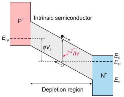 |
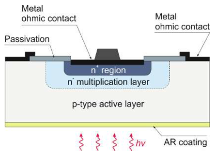
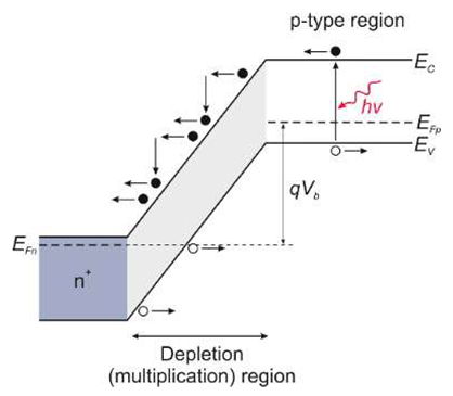
| Avalanche photodiode (APD) The avalanche photodiode detects extremely low-intensity radiation. The n+-n−-p architecture, with controlled doping profiles and a geometry that ensures a uniform electric field, is easy to produce. The high reverse bias generates the depletion layer across the n−region, and photons are absorbed in the p-region. The applied electric field accelerates photogenerated minority carrier electrons at the edge of the depletion region. Their collisions with the crystal lattice cause an avalanche of ionization. This process provides new carriers and causes a rapid increase in current flowing in the reverse direction. The APD offers a combination of high speed, high sensitivity, and high quantum efficiency. |
 |
 |
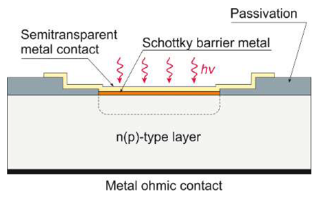
| Schottky barrier photodiode |
- High dynamic range of operation;
-
Low background and floor noise often dominate observations of the weak UV.
Figure 3 shows the classification of ultraviolet detectors.
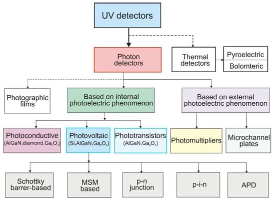
Figure 3.
Classification of UV detectors.
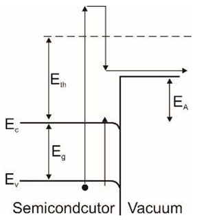
There are two main groups of photon detectors. The first includes those with the external photoelectric phenomenon, which means that photons excite the photocathode to generate photoelectrons, and the external anode registers these electrons. The procedure is used inside the vacuum tube photodetectors, particularly photomultipliers and amplifiers (microchannel plates—MCP).
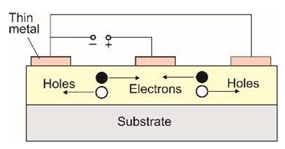
| The photoelectric effect involves the emission of electrons when optical radiation hits a photocathode with sufficiently high kinetic anergy, greater than the vacuum level barrier, to leave the photocathode and be emitted as a free electron. Suppose a large electric field is placed between the cathode and the anode. In that case, the emitted electrons are accelerated in the space between the detector electrodes, and the collecting anode produces a photocurrent proportional to the intensity of the incoming photon. In the photomultiplier tube (PMT), photoemitted electrons impact other dynodes specially placed in the tube, creating a cascade of emitted electrons by a secondary emission process. | 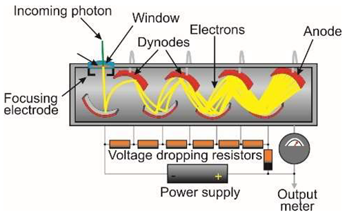 |
 |
| Photoconductor It is an optical radiation-sensitive photoresistor in which incident radiation creates electron-hole pairs in a homogeneous semiconductor material directly across the band gap. This band gap determines the spectral response. During the same phenomenon, a quantum-well photoconductor photoexcites electrons or holes from the potential well in the band-gap regions of the semiconductor. |
 |
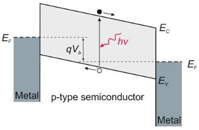 |
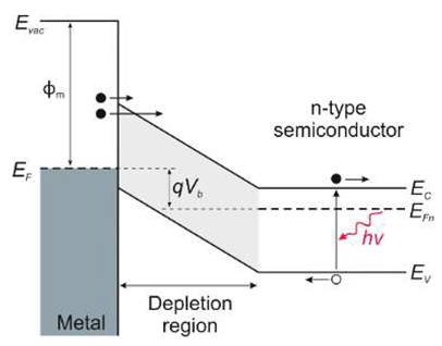
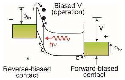
| It is a majority carrier device formed at the metal-semiconductor junction. As with the p–n junction, this junction provides a potential barrier to separate photoexcited electron-hole pairs within the semiconductor or at the metal-semiconductor interface. Compared to a p-n photodiode, a Schottky barrier photodiode has some advantages, e.g., fabrication simplicity (deposition of the metal barrier on the n(p)-semiconductor), lower-temperature diffusion processes, and a higher reaction rate. However, a Schottky junction is generally characterized by a more significant dark current. | ||
 |
 |
|
| Metal-semiconductor-metal (MSM) photodiode This structure is similar to the interdigitated photoconductor, in which Schottky barriers fabricate the metal-semiconductor and semiconductor-metal junctions instead of ohmic contacts. Processing steps nearly identical to those required for making field-effect transistors are used to produce a planar structure with monolithic integration of the MSM photodiode. A lower dark current characterizes this type of design compared to a single Schottky diode and has a faster response speed than a p-i-n photodiode. |
 |
 |
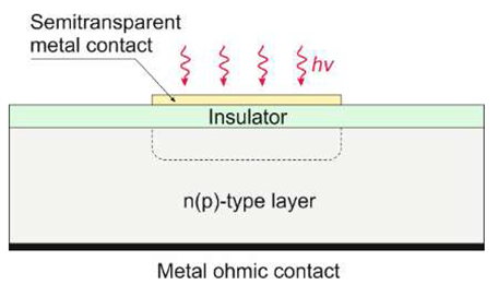
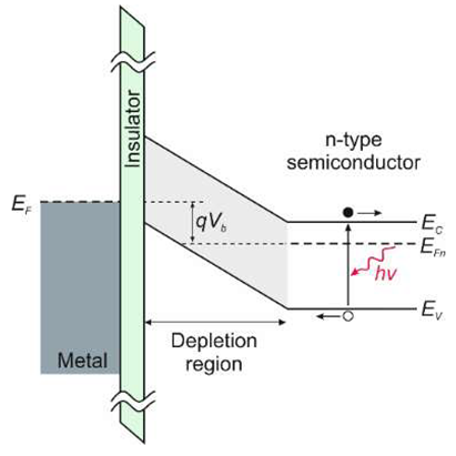
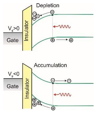
| Metal-insulator-semiconductor (MIS) photodiode This device is built with an insulator separating the metal gate from the semiconductor surface. The thickness of the insulator must not fall below a minimum of about 10 nm. The use of thinner insulation than this leads to the occurrence of tunneling through the insulating layer. A negative voltage relative to the metal electrode creates a depletion region, repelling electrons from the insulator-semiconductor interface. Its “well capacitance” defines the total charge accumulated on a photogate. This capacitance depends on the gate bias, insulator thickness, electrode surface area, and semiconductor background doping. |
 |
 |
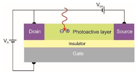
| Photo-FET The device’s configuration is similar to lateral photoconductors, with the MSM architecture forming the source and drain electrodes. The modulation of the channel conductivity is performed using a third gate electrode that is electrically isolated from the semiconductor channel by a thin dielectric layer. The VG gate voltage electronically controls the density of the carrier by modulating the field effect and advantageously switches off the dark current by operating the device in the depletion regime. The incident light activates the conductivity of the device channel by photo-generating the carriers, which then ideally benefit from the photoconductivity enhancement mechanism (photoelectric gain), as in photoconductors. |
 |
 |
2. General Theory of Photodetectors
Photon detectors exhibit a selective sensitivity depending on the incident radiation wavelength related to their unit power (Figure 4a). This is because, ideally, each photon with an energy higher than the bandgap of the semiconductor generates an electron-hole pair (e-h pairs). For a constant radiation power, the number of photons reaching the detector is directly proportional to the wavelength: where Φ is the photon flux, E is the photon energy, h is the Planck constant, c is the light speed, and λ is the wavelength.
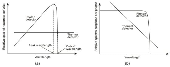
Figure 4.
Relative spectral response for photon and thermal detectors analyzing (
a
) radiation power and (
b
) photon flux.
 where q is the electron charge.
Optical radiation irradiated onto the active surface of the photodetector generates a photocurrent. For a small radiation signal, this current proportionally increases with the radiation power:
where q is the electron charge.
Optical radiation irradiated onto the active surface of the photodetector generates a photocurrent. For a small radiation signal, this current proportionally increases with the radiation power:
 where η is the quantum efficiency and g is the photoelectric current gain.
The quantum efficiency η of a detector is defined by the number of e-h pairs generated by the photodetector per incident photon. Its standardized value is generally less than unity, expressed in percentage. Some absorbed photons may not be registered based on the collected free e-h pairs because some carriers recombine or become immediately trapped. If the radiation penetration depth 1/α (where α is the absorption coefficient) is comparable with the thickness of the semiconductor layer, all photons will not be absorbed. The reflectance of the detector surface and device structure also influences quantum efficiency. That is why reducing the reflections on the semiconductor surface, increasing absorption, and preventing carrier recombination or trapping increase the photodetector’s quantum efficiency.
The number of carriers passing through the contacts per generated pair determines the photoconductive gain. The gain quantitively describes the photodetector’s current response. For example, the photoelectric current gain equals unity for a typical photovoltaic detector.
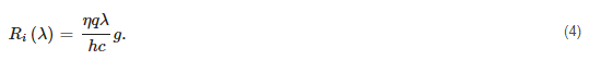
Finally, the spectral current responsivity can be expressed by:
where η is the quantum efficiency and g is the photoelectric current gain.
The quantum efficiency η of a detector is defined by the number of e-h pairs generated by the photodetector per incident photon. Its standardized value is generally less than unity, expressed in percentage. Some absorbed photons may not be registered based on the collected free e-h pairs because some carriers recombine or become immediately trapped. If the radiation penetration depth 1/α (where α is the absorption coefficient) is comparable with the thickness of the semiconductor layer, all photons will not be absorbed. The reflectance of the detector surface and device structure also influences quantum efficiency. That is why reducing the reflections on the semiconductor surface, increasing absorption, and preventing carrier recombination or trapping increase the photodetector’s quantum efficiency.
The number of carriers passing through the contacts per generated pair determines the photoconductive gain. The gain quantitively describes the photodetector’s current response. For example, the photoelectric current gain equals unity for a typical photovoltaic detector.
Finally, the spectral current responsivity can be expressed by:
 The output signal of infrared detectors can be presented as a function of wavelength [6]. In Figure 4a, photon detectors are characterized by wavelength-selective response dependence, and the signal is proportional to the photon arrival rate. Since energy per photon is inversely proportional to the wavelength, the spectral response increases linearly with the wavelength. This growth is possible at the so-called cut-off wavelength, which is determined by the material. It is usually defined when the detector’s response is reduced by 50% of the peak value.
Thermal detectors have a constant responsivity value for analyzing radiation power. However, their photon flux response decreases with increasing wavelength (a decrease in absorbed energy) (Figure 4b). Photon detectors have a higher responsivity and response rate than thermal detectors.
Assuming the same gain values for photocurrent and noise current, the noise current caused by statistical processes of carrier generation and recombination equals [6]:
The output signal of infrared detectors can be presented as a function of wavelength [6]. In Figure 4a, photon detectors are characterized by wavelength-selective response dependence, and the signal is proportional to the photon arrival rate. Since energy per photon is inversely proportional to the wavelength, the spectral response increases linearly with the wavelength. This growth is possible at the so-called cut-off wavelength, which is determined by the material. It is usually defined when the detector’s response is reduced by 50% of the peak value.
Thermal detectors have a constant responsivity value for analyzing radiation power. However, their photon flux response decreases with increasing wavelength (a decrease in absorbed energy) (Figure 4b). Photon detectors have a higher responsivity and response rate than thermal detectors.
Assuming the same gain values for photocurrent and noise current, the noise current caused by statistical processes of carrier generation and recombination equals [6]:
 where G and R are generation and recombination rates, respectively; Δf is the frequency band; and t is the detector thickness.
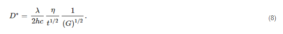
Detectivity D* is the most important parameter of the detector, and it is usually used to determine the detector’s signal-to-noise ratio. Its value is normalized to the detector area and the noise bandwidth and is described by:
where G and R are generation and recombination rates, respectively; Δf is the frequency band; and t is the detector thickness.
Detectivity D* is the most important parameter of the detector, and it is usually used to determine the detector’s signal-to-noise ratio. Its value is normalized to the detector area and the noise bandwidth and is described by:
 Therefore, according to Equations (4) and (5), reaching the following:
 For a given wavelength and operating temperature, the best detector performance has a maximum value of η/[t(G + R)]1/2 term, corresponding to the highest quantum efficiency in the thinnest detector. In addition, the total number of generation and recombination acts per time unit [equal to (G + R) (Aet)] should be as small as possible. At equilibrium, the generation and recombination rates are equal (G = R), and for Ao = Ae, obtaining:
 The noise performance of the detector can also be described by a noise equivalent power (NEP). NEP corresponds to the incident power on the detector that gives a signal-to-noise ratio (SNR) of unity. In terms of responsivity, NEP equals:
 where In and Vn are the current and voltage noises.
Since the noise voltage root mean square (RMS) value is proportional to the square root of the bandwidth, the NEP uses a spectral density with a unit of W/Hz1/2. The lowest values of NEP (NEPmin) are obtained at the wavelength λ with the maximum detector responsivity Rmax(λ). Thus:
where In and Vn are the current and voltage noises.
Since the noise voltage root mean square (RMS) value is proportional to the square root of the bandwidth, the NEP uses a spectral density with a unit of W/Hz1/2. The lowest values of NEP (NEPmin) are obtained at the wavelength λ with the maximum detector responsivity Rmax(λ). Thus:
 The minimum detectable power Pmin can be calculated using the following equation:

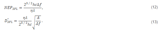
 where ΦB is the flux density of the background photon reaching the detector determined by its field of view (FOV) and the temperature of the background.
Using Equations (4), (6) and (14), the NEP is given by [9]:
where ΦB is the flux density of the background photon reaching the detector determined by its field of view (FOV) and the temperature of the background.
Using Equations (4), (6) and (14), the NEP is given by [9]:

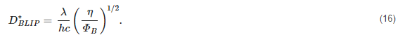 The exemplary graph of the spectral detectivity for a background temperature of 290 K and a 2π steradian detector FOV is presented in Figure 5 [6][13][6,13]. It can be seen that the SFL curve crosses the BLIP line near 1.2 μm. From this, it follows that SFL dominates at wavelengths below 1.2 μm, and that the wavelength dependence of detectivity is weak. However, above 1.2 μm, the influence of background radiation is more significant, and detectivity strongly depends on the wavelength.
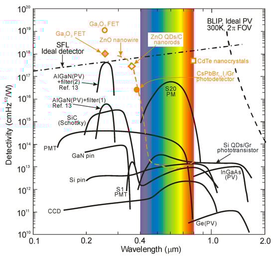
Figure 5. Spectral dependence of detectivity for photodetectors operating at room temperature in the wavelength range of 0.1–2 µm. Designations adopted: PC—photoconductive detector; PV—photovoltaic detector; and PM—photomultiplier. Additional data for AlGaN photodiodes and other various types of photodetectors (pink color) are from the literature.
-
Inadequacy of detectivity specifications based on responsivity and noise (shot noise and generation-recombination noise);
-
Lack of properly refined protocols for accurately determining figure-of-merit for photodetectors (especially for the new-generation of two-dimensional (2D) and quasi-2D material ones).