As the interconnect delay exceeds the gate delay, the integrated circuit (IC) technology has evolved from a transistor-centric era to an interconnect-centric era. Conventional metallic interconnects face several serious challenges in aspects of performance and reliability. To address these issues, nanocarbon materials, including carbon nanotube (CNT) and graphene, have been proposed as promising candidates for interconnect applications.
- nano-interconnect
- carbon nanotube
- graphene
Please note: Below is an entry draft based on your previous paper, which is wrirren tightly around the entry title. Since it may not be very comprehensive, we kindly invite you to modify it (both title and content can be replaced) according to your extensive expertise. We believe this entry would be beneficial to generate more views for your work. In addition, no worry about the entry format, we will correct it and add references after the entry is online (you can also send a word file to us, and we will help you with submitting).
Definition
As the interconnect delay exceeds the gate delay, the integrated circuit (IC) technology has evolved from a transistor-centric era to an interconnect-centric era. Conventional metallic interconnects face several serious challenges in aspects of performance and reliability. To address these issues, nanocarbon materials, including carbon nanotube (CNT) and graphene, have been proposed as promising candidates for interconnect applications.
1. Introduction
The breakthrough development of the semiconductor industry has revolutionized human society, from personal electronic gadgets, commercial and industrial equipment to military and aeronautical facilities. As predicted by Moore’s law, the number of transistors within a chip doubles about every two years, while the cost comes down [1]. According to the International Technology Roadmap for Semiconductors (ITRS) projection, a 10 nm minimum feature size could support a tera-scale chip with a trillion transistors by 2020 [2]. Such phenomenal progress has been achieved through scaling of digital integrated circuit (IC) feature size to smaller physical dimensions.
The ongoing miniaturization of the IC feature size has had a significant benefit in increasing the transistor speed. However, different from the transistor, the interconnect performance would be degraded due to the reduced conduction area and increased scattering probability for electrons [3,4]. Under such circumstances, the chip performance is restricted by the shrinking interconnect dimensions on account of both the interconnect delay and the power dissipation. Moreover, the interconnect reliability has been becoming a more and more important problem, as the ampacity of conventional Cu wire cannot satisfy the increasingly stringent requirements [2,5,6]. Therefore, interconnects have become the major challenge in the design of modern ICs, thereby leading to the transition of IC technology from transistor-centric to interconnect-centric [7]. To address the interconnect challenges for next-generation ICs, diverse improvements of interconnect optimization and design methods have been reported, such as a low-k dielectric structure, three-dimensional integration, and inter-chip optical interconnects [8,9,10].
Nanocarbon materials have attracted much attention since the carbon nanotube (CNT) was discovered by an arc-discharge evaporation method in 1991 [11]. Graphene, a Nobel Prize honored discovery, has further promoted the research in this field [12]. It was found that nanocarbon materials have many extraordinary physical properties. For example, the ultrahigh thermal conductivity of nanocarbon materials can help heat dissipation in high-density integrated systems [13,14,15]. The maximum current-carrying density of a CNT is more than two orders higher than that of Cu wires, thereby mitigating the electromigration-induced reliability problems [16]. It is natural to apply nanocarbon materials as an alternative option to potentially replace Cu for interconnects and passive devices in ICs [17,18,19,20,21,22]. In recent years, there have been many publications in the literature devoted to the design, modeling/analysis, and fabrication/integration of nanocarbon interconnects.
2. Graphene Nanoribbon (GNR) Interconnects
Physically, graphene is a 2D monolayer of carbon atoms packed into a honeycomb lattice, and the quasi-1D graphene nanoribbon (GNR), as shown in Figure 1a, can be utilized as on-chip interconnects [23]. Depending on the edge shape, a GNR can be zigzag, armchair, or chiral (other shapes). The zigzag GNR is always metallic, whereas the armchair GNR is metallic or semiconducting, depending on the number of carbon atoms across its width. Different from the GNR, a CNT’s chirality is defined by its circumferential edge shape. A single-walled carbon nanotube (SWCNT) can be visualized as a seamlessly rolled-up GNR, on the basis of which a novel fabrication method has been developed to unzip the CNT to form a GNR [24]. A multi-walled carbon nanotube (MWCNT) is a parallel assembly of coaxial SWCNTs, and the neighboring shells in an MWCNT are separated by the van der Waals gap.
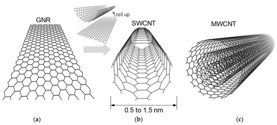
Figure 1. Schematics of (a) monolayer graphene nanoribbon (GNR), (b) single-walled carbon nanotube (SWCNT), and (c) multi-walled carbon nanotube (MWCNT).
3. CNT Interconnects
Similar with GNR, CNT possesses long MFP, high ampacity, and large thermal conductivity [14,16,50,51,52]. Based on the Luttinger liquid theory, Burke firstly developed the transmission line model of a metallic SWCNT interconnect [53]. with the CNT diameter denoted as Dcnt. The number of conducting channels of a metallic SWCNT is 2, and the MFP is usually 1000Dcnt. Although an SWCNT possesses many unit properties and some efforts have been devoted to reducing the SWCNT resistance by doping, an isolated SWCNT is still too resistive for interconnect applications in high-performance ICs [54,55]. It can only be used in some specific applications such as subthreshold circuits and sub-10 nm circuits [56,57,58]. To reduce the CNT resistance, three kinds of CNT interconnects, i.e., monolayer SWCNT, bundled SWCNT, and MWCNT interconnects, have been widely studied, as shown in Figure 2.
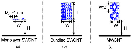
Figure 2. Cross-sectional views of (a) monolayer SWCNT, (b) bundled SWCNT, and (c) MWCNT interconnects.
4. All-Carbon 3-D Interconnects
In general, CNTs grow vertically, whereas graphene is formed horizontally. So, it is natural to develop the 3-D interconnects by combining vertical CNT vias and horizontal GNR interconnects, as shown in Figure 3. Nihei, et al. [91] firstly conceived, designed and realized the experiment to grow an MWCNT via on multilayer graphene. The critical issue to fabricate such “all-carbon” 3-D interconnects is to achieve a low electrical contact between the CNT via and the GNR interconnect. Further, Ramos, et al. [92] introduced a process to selectively grow CNTs on monolayer graphene. They demonstrated that the growth of CNTs would not damage the integrity of graphene and characterized the contact resistance between CNTs and graphene. Zhou, et al. [93] studied the CNT-graphene interface using transmission electron microscope and found that C-C bonding exists between CNT and graphene. Recently, Jiang, et al. [94] comprehensively investigated the fabrication, integration, and reliability of such “all-carbon” 3-D interconnects. Besides, it is worth noting that another “all-carbon” 3-D interconnect scheme, i.e., a dense vertical and horizontal graphene structure, has been demonstrated in [91].
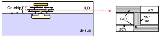
Figure 3. Schematic of all-carbon 3-D interconnect.
Using the finite-element method (FEM), the electrothermal characteristics of all-carbon 3-D interconnects have been studied in [95]. Figure 4a shows the simulation model, which is formed by one horizontal interconnect and two vertical vias. The 3-D interconnect structure is embedded into an interlayer dielectric, whose thermal conductivity is about 0.12 W/m·K. The bottom temperature is assumed as 363 K, and the other boundaries are set as adiabatic. The out-plane electrical conductivity of the MLGNR is 1 S/m. The geometrical parameters are adopted at the 22 nm technology node from the ITRS projection [2]. With a current of 0.4 mA injected, the temperature profiles are plotted in Figure 4b–d. In the simulation, a 1 nm-thick thin plate was used to capture the influences of contact resistance. Due to the impact of quantum contact resistance, all-carbon 3-D interconnect is more resistive than Cu counterpart, thereby increasing the temperature rise. On the contrary, the CNT vias help heat dissipation from hotspots to the bottom layer. Therefore, the maximum temperature is slightly increased with the implementation of all-carbon 3-D interconnects. The results also imply that CNT vias are more suitable to be placed near bottom layer.
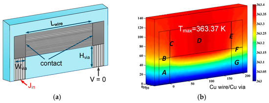
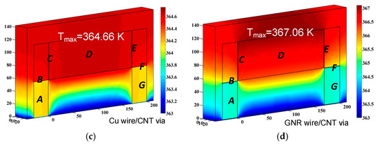
Figure 4. (a) Schematic of a simulation model. (b–d) Temperature profiles of Cu, SWCNT vias/Cu wire, and SWCNT/MLG interconnects [95].
5. Cu-Nanocarbon Interconnect
5.1. Cu-Graphene Interconnect
During the past decades, tremendous progress has been made in the fabrication/integration of nanocarbon interconnects. However, the gap between theoretical studies and practical applications still exists. For example, the assumption of closed packed CNTs is invalid as the density of CNTs still cannot satisfy the requirements [96]. Also, the application of MLGNR interconnects encounters a serious challenge, i.e., graphene tends to behave more like graphite as the number of graphene layers increases [97]. In this perspective, Cu/low-k interconnect may be still a good choice for next-generation ICs [98].
In the application of Cu/low-k interconnect, a highly resistive diffusion barrier layer is required to prevent the diffusion of copper atoms into substrate. This barrier layer would occupy a certain area, thereby decreasing the conduction area of interconnects and increasing the effective resistivity. More importantly, the barrier layer thickness cannot scale as rapidly as the interconnect dimensions [4]. This problem becomes more and more serious with the technology advanced. To resolve this problem, graphene, the thinnest 2-D material in nature, has been proposed as the ultimate barrier layer [99,100,101]. It has been demonstrated that graphene barrier layer can help improving the breakdown current density, enhancing the electromigration lifetime, increasing the Cu grain size, and reducing the scattering probability at the surface [102,103,104,105,106]. Moreover, low-temperature deposition techniques for producing graphene on Cu and dielectric implies that the fabrication of graphene barrier layer can be compatible with traditional CMOS technology [101,104,107,108].
5.2. Cu-CNT Composite Interconnect
Generally speaking, nanocarbon and conventional metals have their own pros and cons for interconnect applications. For instance, nanocarbon has high ampacity, but their conductivity is still low due to fabrication limits. On the contrary, the fabrication and integration processes of metal interconnects are mature, but the ampacity of metals cannot satisfy the requirements [2]. Subramaniam, et al. [111] attempted to advance a possible solution to this problem by co-depositing Cu with CNTs, i.e., Cu-CNT composite interconnect. It was experimentally demonstrated that Cu-CNT composite interconnect can achieve a balance between performance and reliability. This is, such Cu-CNT composite interconnect possesses a 100 times higher ampacity, but comparable conductivity than the Cu counterpart. The presence of CNTs inside Cu wire can also alleviate the electromigration void growth rate by about four times, which is due to large Lorenz number of the CNTs [112,113].
6. Conclusions
The current status of research on nanocarbon interconnects from a modeling perspective has been reviewed in this work. Several typical nanocarbon interconnects have been evaluated and discussed. It is demonstrated that nanocarbon interconnects are theoretically superior to their Cu counterparts. However, due to the fabrication limits, the electrical performance of nanocarbon interconnects may be much worse than their theoretical estimations. Cu-nanocarbon interconnects, including Cu-graphene and Cu-CNT composite interconnects, may be a practical solution to meet the near future challenges. With the IC feature size scaling down to sub-10 nm, however, nanocarbon interconnects are the most promising schemes. This is to say, in long-term applications, Cu-nanocarbon interconnects may be used together with the ultimate nanocarbon interconnects.
This entry is adapted from the peer-reviewed paper 10.3390/app9112174