1000/1000
Hot
Most Recent
 +1 point
Recent studies on bias-temperature instabilities (BTI) in D- and E-mode GaN transistors are reviewed here, focusing on BTI mechanisms in fully recess-gate E-mode GaN transistors.
A combination of wide band gap (3.4 eV), high breakdown electric field (3 MV/cm), decent thermal conductivity (>1.5 W/cmK), and high saturation velocity (~107 cm/s) of electrons makes GaN an ideal material for high-power semiconductor devices [1][2][3]. Indeed, GaN-based high electron-mobility transistors (HEMTs) with high cut-off frequency and high breakdown voltage (VBD) enabled development of new generation of power amplifiers implemented in wireless communication, satellite, and radar systems commercially available already a decade ago [4]. More recently, GaN HEMTs have been also applied as switching devices for power converters. Despite relatively immature technology, the state-of-the-art GaN switching devices have shown lower ON-state resistance (RON) for given VBD compared to current power devices based on Si [5][6][7]. Intensive R&D effort in the last decade pawed the way to emerging of highly efficient and compact GaN-based power converters in the market [8]. However, the issues related to stability and reliability of GaN power switching devices hamper a more dramatic commercial success of this technology. To take advantage of outstanding properties of GaN material, a key task is to gain a fundamental understanding of the parasitic and degradation mechanisms that negatively affect the performance and long-term reliable operation of these devices. This represents a rather difficult task, keeping in mind the unique properties of GaN-based materials (wide-band gap nature, piezoelectricity) and high electric field combined with dissipating power of the operating devices. In addition, GaN heterostructures for lateral transistors are grown on foreign substrates. Therefore, a variety of extended defects are present in the device active region.
In GaN MISHEMTs, BTI represents one of the biggest reliability concerns. This is due to relatively high density of traps located in the gate stack, being a consequence of unavailability of high-quality native oxides for GaN-based semiconductors and complexity of the dielectric/III-N interfaces. As a result, considerable BTI with VTH instabilities ranging from 100 mV up to several V have been commonly reported for GaN MISHEMTs in the literature [9][10]. For D-mode MISHEMTs, NBTI is expected to be a major concern as the device is commonly biased in OFF-state with VGS < 0. Indeed, several researchers have reported NBTI to induce negative VTH drift strongly enhanced by temperature [10]. Although PBTI may be considered less problematic in these devices, many studies have been devoted to PBTI investigations in D-mode MISHEMTs with an aim to analyze the underlying mechanism of VTH drift [11]. The dynamics of the PBTI in GaN MISHEMTs was found to differ from that known for Si metal-oxide-semiconductor field-effect transistors (MOSFET), mostly because of coaction of different trapping states in the gate stack, nontrivial defect dynamics, and electron transport over the existing barrier affecting the trapping dynamic [12]. For E-mode MISHEMTs, PBTI is clearly the major concern as the positive VGS drives the device into ON-state. Dramatic VTH drifts upon PBTI testing has been reported in the literature [13]. In addition, specific designs for achieving E-mode behavior for MISHEMTs, such as application of InGaN/AlGaN double barrier layer, have been shown to result in a unique mechanism of PBTI [14]. GaN transistors with fully recessed barrier (also known as recessed gate hybrid MISHEMTs [15]) represent a special design of E-mode GaN devices, referred here to as GaN MISFETs. A complete etching-away of the barrier layer under the gate greatly simplifies the interpretation of the BTI data. Available studies investigating BTI in GaN MISFETs consistently indicate that both PBTI and NBTI need to be concerned. Moreover, it seems that dielectric bulk traps with specific distribution play a major role affecting the PBTI as well as NBTI behavior [16][17].
Majority of BTI studies in GaN MISHEMTs are focused on PBTI of D-mode devices. This is because of great advancements achieved in the technology of non-recessed or partially recessed AlGaN/GaN MISHEMT switching devices. These studies allowed for deeper analysis of the VTH drift mechanisms under positive bias stress, even though such devices are not expected to operate at such conditions. In fact, only a limited number of studies investigating PBTI in E-mode GaN MISHEMTs are available in the literature, which is simply because only a few design concepts of non-recessed E-mode MISHEMTs are available [18][19][20][21][22]. On the other hand, NBTI represents a major concern in the D-mode GaN MISHEMTs used, e.g., in the cascade configuration. However, due to availability of reliable and stable SB HEMTs, less interest has been given to NBTI investigations in D-mode GaN MISHEMTs. A comprehensive review of the PBTI mechanisms in GaN MISHEMTs can be found elsewhere [12]. Here, we will only discuss the most relevant research works aiming for a deeper understanding of the BTI mechanisms in D- and E-mode GaN MISFETs.
An often-used approach to process lateral E-mode GaN switching transistor is to fully recess the AlGaN barrier layer under the gate, while existing 2DEG in the source-to-gate and gate-to-drain regions provide a low access resistance. The MIS gate structure of fully recessed GaN devices resembles that of Si MOSFETs and many approaches developed for BTI investigation in Si devices have been adopted also for description of PBTI and NBTI issues of GaN MISFETs. Universal recovery model developed for Si MOSFETs [23] have been widely employed to describe the PBTI [16] as well as NBTI [17] behavior of GaN MISFETs. Although dielectric/GaN interface traps (IT) plays some role, there seems to be a general agreement that dielectric bulk traps (OT) have dominant impact on the PBTI and NBTI mechanism.
Comprehensive analysis of PBTI in fully recessed GaN MISFETs with plasma-enhanced atomic layer deposited (PEALD) SiN and ALD grown Al2O3 gate dielectric was performed by Wu et al. [16] . Due to observed lack of correlation between ID-VGS hysteresis (thus ΔVTH) and the density of interface traps (DIT ) distribution measured by G-ω method, the authors employed PBTI stress-recovery tests using the measure-stress-measure (MSM) technique [9]. It was found that ΔVTH transients for different VG,stress (Figure 1a,b) can be fitted using power-law relation [16] in the whole range of tstress with time exponent n in the range of 0.1–0.02. Despite notably higher DIT, devices with Al2O3 showed about 10-times lower ΔVTH compared to those with SiN, when benchmark at tstress = 2 s depicted by the black arrows in Figure 1a,b. The voltage exponent γ of 1 and 2 and Ea of 0.57 and 1.02 eV was observed for devices with SiN and Al2O3, respectively. The recovery ΔVTH transients obeyed empirical model of universal relaxation [23]
(1)
(2)
where R and P represent recoverable and permanent degradation ascribed to different types of defects, trelax is measured form the end of last stress phase, ξ = trelax/tstress is the universal relaxation time, B is the scaling parameter and exponent β represents the dispersion parameter. From the fitting of Equations (1) and (2) to the ΔVTH recovery transients (Figure 1c), devices with Al2O3 gate dielectric were found to show lower recoverable and permanent degradation and faster dielectric defect discharge. Such behavior was attributed to presence of OT Gaussian distributions depicted. In the case of SiN, a wider distribution of OT levels (σ ∼ 0.67 eV), centered below the conduction band of GaN (EC−0.05 eV) are easily accessible by the channel carriers already at a low VG,stress. In contrast, Al2O3 gate dielectric was proposed to feature a narrower distribution of OT (σ ∼ 0.42 eV) located far from the conduction band edge of GaN (EC + 1.15 eV), explaining the improved PBTI behavior in devices with ALD grown Al2O3 gate dielectric compared to those with SiN.
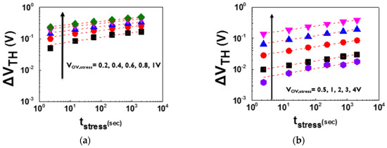
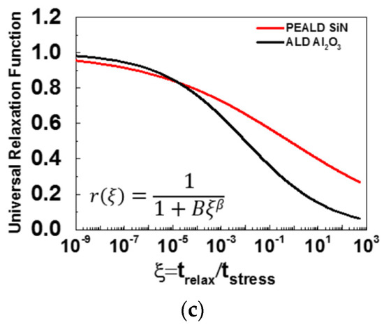
Figure 1. ΔVTH transients for different tstress of fully-recessed MISFETs with (a) plasma-enhanced ALD (PEALD) SiN and (b) ALD Al2O3 gate dielectric in a logarithmic–logarithmic scale. Dashed lines represent the power-law fits (Equation (6)) to the data. (c) Recovery transients fitted with the universal relaxation model (Equations (7) and (8)) showing faster relaxation for the device with Al2O3 gate dielectric. Copyright © 2020 IEEE. Reprinted, with permission, from Ref. [16].
Dominant impact of dielectric OT on the VTH instabilities has been proposed also by other studies. Bisi et al. [24] studied PBTI stress-recovery kinetics in Al2O3/GaN MIS capacitors grown by in-situ MOCVD by means of combined IG transient, capacitance-voltage (CV) and capacitance MSM technique. In the low-field (oxide electric field <3.3 MV/cm) regime, IG stress and recovery transients were found to obey power-law with α ~ 1, suggesting trapping and de-trapping of near-interface OT. In contrast, high-field regime (>3.3 MV/cm) was characterized by the onset of the gate leakage current promoted by OT and significant positive flat-band voltage (VFB) shift, suggesting enhanced charge trapping of OT, as also revealed by very slow recovery transients [24]. Acurio et al. [25] studied PBTI in a fully recessed-gate GaN MISFET with PECVD SiO2 gate dielectric using ID-VGS measurements interrupting the stressing and recovery. Similar to previous results, power-law dependence of ΔVTH on tstress was observed. Furthermore, trapping rate
exhibited a universal decreasing behavior as a function of the number of filled traps. Stress-induced ΔVTH was fully recovered by applying a small negative voltage and the recovery dynamics (monitored in time window between 1 s and thousands of seconds) was found to be well described by the superimposition of two exponential functions. These emission processes were associated with two different OT. The slower trap revealed EA of 0.93 eV and the faster trap exhibits large spread in EA ranging from 0.45 eV to 0.82 eV. VTH recovery with two different time constants have been also observed also by Iucolano et al. [26]. By measuring the hysteresis of ID-VGS characteristics with different VGS,max (VDS = 0.1 V), partial VTH recovery was reached after a few seconds, however, a complete VTH recovery required more than one day of unbiased storage. Based on the numerical simulations, the fast and slow recovery processes were associated with the emission from IT and OT localized above the GaN conduction band energy, respectively.
In fully recess-gate MISFETs, the drain-edge of the gate terminal represent another critical region concerning the BTI, as trapping states formed close to interface between the dielectric and the barrier side-wall can negatively affect VTH as well as RON stability. In the study of Chini and Iucolano [27], E-mode GaN MISFETs were subjected to PBTI in the switching-mode operation and VTH and RON drift was monitored simultaneously using special designed pulsed setup [27]. Apart from positive VTH drift related to IT traps under the gate region, also VTH drift linked to a localized trapping in the drain-edge of the gate terminal was identified. Further, the observed increase in RON was associated with a hole-emission process taking place in the gate-drain access region within the C-doped buffer layer.
Current understanding of NBTI in E-mode GaN MISFETs is quite limited and some controversy exist in the observed behavior. In one of the first studies, Sang et al. [28] compared VTH drifts under negative VG stress in the D-mode MISHEMTs and E-mode GaN MISFETs with ALD Al2O3 gate dielectric. For the latter, the positive stress-induced VTH shift was observed, which was attributed to metal gate electron injection into OT and following redistribution of the trapped charge towards the GaN channel via trap-assisted tunneling. Later, Guo and del Alamo [29] performed a more detailed investigation of NBTI in SiO2/Al2O3/GaN MISFETs subjected to negative VGS stress with different amplitude, duration, and temperatures. Stress-induced VTH shift was found to progress through three regimes. Under low-stress (low VGS,stress, low T, short tstress), ΔVTH was negative and recoverable due to electron de-trapping from pre-existing OT. Under mid-stress (low VGS,stress, high T, longer tstress), positive and recoverable ΔVTH was observed, i.e., behavior similar to that reported by Sung et al. [28]. However, the cause of this effect was attributed to electron tunneling from valence band (VB) to trap states in the GaN channel under the gate edges, also referred the as Zener trapping in the literature [30]. For high-stress (VGS,stress < −30 V, RT), non-recoverable negative ΔVTH was observed and ascribed to generation of new IT.
Recently, Guo and del Alamo [17] presented a comprehensive study of BTI in GaN MISFETs under moderate positive and negative gate bias stress (VG,stress = +5 and = 5 V) using fast ID-VGS measurements interrupting the stressing. VTH evolution was monitored during the stressing and recovery phase, followed by full recovery of VTH to pre-stress value. For positive VG,stress, positive ΔVTH drift was observed, which increased with stressing voltage. Nearly symmetrical behavior with negative VTH drift was observed for NBTI. For both stress conditions, the VTH time evolution was found to follow power-law model during the stressing and universal relaxation model (Equations (1) and (2)) during the recovery. Therefore, the authors proposed that NBTI and PBTI are caused by the same mechanism, which is the electron trapping/de-trapping in preexisting OT that form a defect band close to the dielectric/GaN interface [17]. The authors assumed the defect band extending the energies above the GaN conduction band (CB) edge and below the surface Fermi level at VGS = 0 V. This means that some trap states are empty while some are populated with electrons at VGS = 0 V. During the stress phase, the electron occupation of OT increases or decreases depending on the sign of VG,stress, resulting in VTH in positive or negative direction, respectively. In the recovery process, the trap occupation returns to the state corresponding to VGS = 0 V.
Apparent positive stress-induced VTH drift under NBTI was observed also in studies of Hua et al. [31][32] and He et al. [33] in E-mode GaN MISFETs with LPCVD-SiNx/PECVD-SiNx/GaN gate stack. The PECVD SiNx interfacial layer (thickness of ~2 nm) grown at low temperature was employed to improve the gate stability and reliability [31]. NBTI was performed at VGS,stress = −30 V (VDS = 0 V) at temperatures of 25 and 150 °C [31][32]. While relatively low positive VTH drift (<0.2 V) was observed at 25 °C, it increased to ~0.4 V for stressing at 150 °C. The positive VTH drift was ascribed to metal electrode injection into OT at negative VGS. In the upcoming work of this group [34], VTH stability under OFF-state step-stress in similar devices was compared for different VGS (0 and −20 V) applied during the stressing, using the same gate-to-drain voltage (VGD). Similar to a previous study, relatively low and recoverable positive VTH drift was observed for step-stress with VGD up to 200 V and VGS = 0 V. However, a substantially larger VTH drift (~2 V) appeared for VGD > 100 V when more negative VGS was applied during the step-stress. The larger VTH drift was explained by a hole-induced degradation model. Here, holes generation via impact ionization [35] or Zener trapping [30] is assumed in the high-field gate-to-drain region in the OFF-state. For stressing with negative VGS, the generated holes can flow to the gate and are assumed to generate new OT in the gate dielectric, similar to time-dependent dielectric breakdown (TDDB) mechanism [36]. The effect of holes generation on the apparent positive VTH drift was further confirmed by UV light illumination of the devices subjected to OFF-state stressing [37]. However, the observed stress-induced positive shift of VTH was ascribed to electron trapping during the measurement of ID-VDS characteristic, interrupting the stressing. This clearly illustrates the advantage of the MSM techniques, where VTH drift is sampled quickly after the stress interruption, rather than extracted from slower measurement of the ID-VGS characteristic.
To mitigate the reverse-bias induced gate degradation in SiNx/GaN MISFETs, Hua et al. [38] recently processed the transistor with channel converted from GaN to crystalline GaOxN1−x under the gate. The oxynitride with higher bandgap (4.1 eV) compared to GaN (3.4 eV) provides also VB offset in respect to GaN (0.6 eV), which acts as an energy barrier for holes. This barrier effectively suppresses the injection of the generated holes into the gate, improving the gate stability and robustness [37]. Robustness of VTH stability upon reverse-bias stress in SiNx/GaOxN1−x/GaN MISFETs can be further enhanced by varying the substrate termination [39].
The presented studies clearly point to dominant effect of OT on PBTI as well as NBTI in GaN MISFETs. This means that most commonly used dielectric materials (Al2O3, SiO2, SiN) with research [16][17][31][24][25][26][27][28][32][38] as well as industry [40] graded quality contain relatively high density of OT. Apart from BTI issues, these defects represent the concern also in relation to TDDB. However, further research work focusing on the enhanced MSM technique, which allows a detailed study of capture/emission processes in the μ-s range is clearly necessary. Detailed knowledge of the OT origin can, in turn, facilitate their effective suppression via optimization of the dielectric growth technologies.