Submitted Successfully!
To reward your contribution, here is a gift for you: A free trial for our video production service.
Thank you for your contribution! You can also upload a video entry or images related to this topic.
Version Summary Created by Modification Content Size Created at Operation
1 I have modifyied the subsection of subject, becouse our paper content is more related to the Nanotechnology + 228 word(s) 228 2020-09-24 08:11:30 |
2 format correct + 2213 word(s) 2441 2020-10-19 04:36:33 | |
3 format correct + 1 word(s) 2442 2020-10-21 11:28:36 |

Video Upload Options

Do you have a full video?

Confirm

Are you sure to Delete?
Cite
If you have any further questions, please contact Encyclopedia Editorial Office.
Junaid, M.; Md Khir, M.H.; Witjaksono, G.; Ullah, Z.; Tansu, N.; Saheed, M.S.M.; Kumar, P.; Hing Wah, L.; Magsi, S.A.; Siddiqui, M.A. Graphene-Based Light Emitting Functional Devices. Encyclopedia. Available online: https://encyclopedia.pub/entry/2435 (accessed on 18 April 2024).
Junaid M, Md Khir MH, Witjaksono G, Ullah Z, Tansu N, Saheed MSM, et al. Graphene-Based Light Emitting Functional Devices. Encyclopedia. Available at: https://encyclopedia.pub/entry/2435. Accessed April 18, 2024.
Junaid, Muhammad, M. H. Md Khir, Gunawan Witjaksono, Zaka Ullah, Nelson Tansu, Mohamed Shuaib Mohamed Saheed, Pradeep Kumar, Lee Hing Wah, Saeed Ahmed Magsi, Muhammad Aadil Siddiqui. "Graphene-Based Light Emitting Functional Devices" Encyclopedia, https://encyclopedia.pub/entry/2435 (accessed April 18, 2024).
Junaid, M., Md Khir, M.H., Witjaksono, G., Ullah, Z., Tansu, N., Saheed, M.S.M., Kumar, P., Hing Wah, L., Magsi, S.A., & Siddiqui, M.A. (2020, October 08). Graphene-Based Light Emitting Functional Devices. In Encyclopedia. https://encyclopedia.pub/entry/2435
Junaid, Muhammad, et al. "Graphene-Based Light Emitting Functional Devices." Encyclopedia. Web. 08 October, 2020.
Graphene-Based Light Emitting Functional Devices
Edit

Light emissions from graphene-based active materials can provide a leading platform for the development of two dimensional (2-D), flexible, thin, and robust light-emitting sources. In this study, we present a comprehensive review of recent developments in graphene-based light-emitting devices. Light emissions from graphene-based devices have been evaluated with different aspects, such as thermal emission, electroluminescence, and plasmons assisted emission. Theoretical investigations, along with experimental demonstration in the development of graphene-based light-emitting devices. Moreover, the graphene-based light-emitting devices are also addressed from the perspective of future applications, such as optical modulators, optical interconnects, and optical sensing. Finally, this review provides a comprehensive discussion on current technological issues and challenges related to the potential applications of emerging graphene-based light-emitting devices. 

Nanotechnology Nanomaterials Nanophotonics

1. Introduction

Graphene is a single layer honeycomb structure of carbon lattice [1] with many interesting behavior and characteristics [2]. It is considered the most promising material for engineering design due to its extraordinary electrical, mechanical, and chemical properties [3][4][5]. Since 2004, the exfoliation of single-layer graphene [6] has been investigated and explored in every field of science. Additionally, an exponential increment in terms of publication numbers was perceived with substantial results [7][8]. Graphene as an attractive material has been extensively researched in many fields of electrical and electronic engineering, such as touch screens, light detectors, transparent conductors, photovoltaic cells, and energy systems [9][10][11]. Besides, the optoelectronic properties of graphene-based materials are being highly investigated for the application of optoelectronic devices [12]. The direct bandgap opening [13][14][15], strong light-matter interaction [16], photoluminescence [17], electrons field emission [18], and the evidence of emission radiation from graphene make it a promising material for the future generation of optical devices to produce a thin, flexible, and lightweight optoelectronics device [19].

In the context of light-emitting diode (LEDs), the existing LEDs technology is considered quite mature, even at the consumer end. LEDs have already been applied in several fields, including signage, display backlight, general illumination, and communications [20][21]. LEDs have high-performance characteristics, such as low power consumption, high efficiency, high-speed response, low operating voltage (< 4 V), current (< 700 mA) characteristics, and small outline dimensions (< 10 mm to 10 mm) [22]. Solid-state light-emitting devices (LEDs) are classified into two main streams: organic (OLEDs) and inorganic LEDs. Conventional inorganic LEDs are composed of brittle or hard powdery material, i.e., silicon, phosphor, lens, and glass. Many key research areas in LED designing, such as quantum efficiency of the active region, current-flow design, resistive losses, electrostatic discharge stability, and optimization of luminous flux per LED package, need improvements [23]. However, flexible and transparent light-emitting devices with a small footprint are of key focus. The development and manufacturing of OLEDs carried out in recent years are still facing drawbacks [24]; for example, the panel fabrication at high-temperature conditions and to incorporate flexible substrate PET (polyethylene terephthalate). ITO-based electrodes are too stiff for the development of flexible OLEDs [25]. The graphene is also considered an alternative material to ITO due to excellent electrical conductively, transparency, and chemical and thermal stability [26]. Graphene and doped graphene, such as transparent electrode [27], with nanowire [28], CNTs, and SWCNTs [29], have also been studied with improved LEDs performance in term of current spreading enhancement [30] and ohmic contact formation with reduced growth temperature [31].

Moreover, the light emission from different graphene structures, such as single and multilayer graphene [32], reduced graphene oxide [33], graphene nanoribbons [34], and quantum dots [35][36][37] has been reported. The emission radiation in spectral range (NIR) near-infrared to the visible region (VIS) and grey body radiation from electrically drive graphene-based devices have also been demonstrated practically. Several theoretical attempts have also been made to justify the light emission from graphene and related structures, where the corresponding emission is explained by the thermal emission radiation [38], plasmons assisted emission [39], and electroluminescence [40]. Besides, the light emission from graphene was also demonstrated with numerous potential applications, such as light-emitting devices, sensors, bioimaging, drug delivery, optical modulators, and optical interconnects [41][42][43].

Thermal emission from electrically driven graphene devices was also reported in the spectral region from infrared (IR) to visible range [44]. Thermal emissions from the graphene layer were ascribed to local heating, with almost the entire spectrum of grey body radiations, where a small fraction of energy about (~10−6 part) is converted into light emissions [32][45]. The sustainable high current density (107 A.cm−2) in micron-sized CVD graphene as compared to conventional tungsten filament (~100 A.cm−2) and with low thermal mass three times smaller in the magnitude of silicon cantilever offers the prospect of high-frequency operation. Likewise, there is constant demand for the development of new IR sources with low cost, safe, and portable safe gas sensors, particularly for mine security. The existing IR sensors use conventional incandescent light sources with several limitations such as lifetime, wavelength, time response, excessive power consumption, and the requirement of explosion-proof casing in a flammable environment. MEMS-based electromechanical silicon emitters, as an alternative IR source, also exhibit low response time up to ~100 Hz modulation frequencies [46]. Solid-state LEDs offer more advantages, particularly in terms of higher modulation speed. However, the radiative efficacy of the LED operated in infrared is limited by the non-radiative Auger recombination [47]. The infrared emission from LED, an intrinsic process, mainly depends on charge carrier density and particularly on narrow semiconducting bandgap. The combination of narrowband semiconductors with a higher refractive index was used for the fabrication, which binds the photon escaping mechanism and limits overall efficiency [48]. However, the demonstration of thermal emission from a large-area graphene layer coupled with extraordinary thermal conductivity offers a prospect for the high-efficiency IR light source.

The realization of ultrafast plasmons-based optical signal source at the nanoscale is considered as a longstanding goal, the potential of the graphene-based emitter to revolutionize optoelectronics, thus allowing ultrafast optical signal processing for communication [49]. When the electron beam is exposed to the optically excited surface plasmons of graphene, the unidirectional, chromatic, and tunable emission from IR to X-ray was realized from the graphene [50][51][52]. The theoretical investigation and experimental demonstration of this mechanism predict the existence of plasmons at VIS and IR wavelengths [53]. Besides, the plasmons-assisted light emission from graphene in VIS, and even shorter wavelength was illustrated by the interaction of surface plasmons and charged particles [50][52]. Significantly, the 2D quantum Čerenkov effect (ČE) can also be achieved in graphene, due to the unique properties of high field confinement, surface plasmons, and low phase velocity. The quantum ČE effect in 2D graphene refers to the emissions when shockwave plasmons are excited by the hot carrier in manners as in three-dimensional (3D) medium. The 2D quantum ČE leads to light emission from the VIS to the IR region, where surface plasmons are coupled as photon radiation due to impurities or roughness in graphene structures [54].

Graphene can also produce the luminescence effect by inducing an energy bandgap. Therefore, there are two possible ways to induce bandgap in graphene: the first is by cutting it into ribbons or quantum dots, and the second is by chemical or physical treatments by connectivity reduction of the π-electron network [55]. The electroluminescence (EL) effect observed from graphene and graphene-related structure is quite interesting, as graphene can be used as an active material for light-emitting devices. The phonon-assisted EL emission in the VIS region was also reported from the electrically biased graphene supported on a substrate [56]. The VIS emission from graphene was also demonstrated by the excitation of electron tunneling current in STM (scanning tunneling microscope) using a voltage biased tip, which is attributed to hot electroluminescence [57]. In addition, the tunability of the EL emission spectrum for the entire visible spectrum was demonstrated by the application of gate voltage, which is quite challenging in the modern solid-state (LEDs) industry [58]. Lastly, graphene-based light emitting devices classified based on the light-emitting mechanisms shown in Scheme 1.

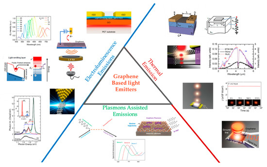
Scheme 1. Graphene-based light-emitting functional devices, where the emission radiation from graphene has been ascribed to thermal, electroluminescence, and plasmons assisted emissions [57][59][60][61][62].

2. Plasmons-Assisted Emissions from Graphene

There is increased interest on highly integrated optoelectronic devices with surface plasmons polarities and nanoscale light emitters [63]. In recent studies, it has been demonstrated that the ability of graphene plasmons (GPS) can be utilized as a platform for strong light-matter interaction [64][65][66]. Furthermore, the dynamics of highly confined light with tunable GPS makes the graphene an extremely promising candidate for the design of light emitters at the nanoscale [67][68]. Besides, the strongly-confined and high momentum graphene plasmons can enable the development of tunable, monochromatic, highly directional, and high frequency (1014–1015 Hz) light-emitting sources with relativity low energy electrons [69]. Additionally, the high-quality light emitter with a small footprint with X-ray and extreme ultraviolet radiation is extremely exciting in the research perspective of medical engineering and natural science. However, the graphene plasmons-based short-wavelength emitter has not been investigated, as compared to other graphene-based promising applications [70].

Besides, the tunable, monochromatic, and highly directional light emission from the graphene layer with the interaction of electrons and plasmons has been reported by Liang and colleagues [71]. The schematic diagram of the graphene plasmon-based radiation source is shown in Figure 1a,b. The generation of highly directional X-ray emissions from modestly relativistic electrons is presented, which does not require additional neutron shielding. Moreover, the low energy electrons are possibly generated in a device on-chip for the frequency conversion mechanism. In design configuration, the graphene sheet was staked on a dielectric substrate with a grating structure, wherein the dielectric substrate was utilized to sustain graphene plasmons. The graphene layer was excited by coupling a focused beam when the electron beam was launched in parallel with the surface of the graphene. The consequent interaction between the graphene plasmons field and low energy electrons induce transverse electrons oscillations [71]. Therefore, soft and hard X-ray radiation from the graphene surface was accomplished without any further acceleration stage; the various frequency conversion regions are shown in Figure 1c,d. Specifically, the plasmons are quasiparticles interacting with modestly relativistic electrons, which govern by the electron-phonon interaction, the same as fundamental rules for the radiation process. However, different results have been reported because the graphene plasmons generate much higher momentum than the energy of photons at the present state. Additionally, graphene plasmons have longitudinal field components, which photons do not have. Consequently, the electron-plasmons scattering was different from the electron-photon scattering, as stated by the standard Thomson or Compton effect [71].

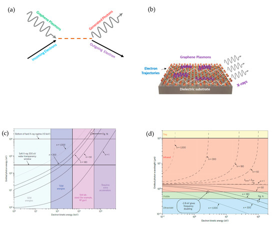
Figure 1. Graphene plasmonic-based source for short wavelength radiation. (a) shows the electrons-plasmon interaction, where the white dotted line demonstrates the free electrons interacting with plasmons glowing with blue and red bars, (b) illustrates the process of graphene plasmons emission from hot carriers. (c) The soft and hard X-ray radiation from graphene-based free electrons radiation source was achieved without any acceleration stage, with various frequency conversion region, the lines correspond to confinement factor (n = 1,50… 1,000) where n = 1 is shown as a reference. (d) shows the up-converting (black line) and down convection (dash line) of related frequency from graphene-based free electrons source. It is observed that the coupling of phase velocity of graphene plasmons velocity and electrons velocity cause the down-conversion of frequency [71].

In related research, Pavel A. Cherenkov showed light radiation from charged particles when the charge moves faster than the phase velocity of light in the medium. However, the requirement of relativistic partials makes light emission unreachable at nanoscale optoelectronic devices [72]. Notably, the existence of high-velocity hot carriers (Fermi velocity ~106 ms–1) is possible, even in graphene sheets larger than 10 μm large [73]. However, the plasmons in graphene show extremely low phase velocity (a few hundred times slower than the speed of light) [74][75]. Therefore, the frequency matching between plasmons and hot carriers is possible via electrical excitation, which enables the high rate of GPs emissions. In addition, the propagating charge carrier inside the 2D graphene layer could efficiently excite GPs via the Cˇerenkov emission (CˇE) process. Significantly, higher rates of GPs emission have been observed in CˇE than previous studies on phonons/photons [74][76].

Additionally, the surface plasmons create energy levels higher than 2EF, which exceed the energy level of photon emission and enable plasmons emission from terahertz to infrared and possibly invisible emissions spectra. Likewise, the tunability of energy levels from the implication of external electrical excitations can improve radiation parameters such as direction, spectrum, and intensity. More significantly, the emission radiation behavior of graphene-based material such as high-frequency radians [32][83][77], saturation current [84][78], black body radiations [79], and tunable spectrum [80] can be explained by the following transition phenomenon. The quantum Cherenkov effect can be defined as the process of spontaneous emission from the charger carrier emitting into graphene plasmons, which can be calculated by Fermi’s golden (GPs) [81][82]. In related studies, Ido Kaminer et al. developed the quantum Cerenkov theory for plasmonic emission radiations and analyzed the phenomenon of novel Cerenkov-induced plasmonic emission. The graphene plasmons can provide a platform to overcome limitations related to relativistic particles for plasmonic emitters through the high field confinement and low phase velocity.

Moreover, the coupling of plasmons and charge carriers inside the graphene layer enables the highly efficient two-dimensional Cerenkov emission, where versatile, tunable, and ultrafast conversion from electrical signal source can be used to overcome the limitations. Figure 2a shows the graphene plasmon emission from a hot carrier inside the graphene. The white arrow shows that the hot carriers make a transparent blue shape, which excites graphene plasmons, as shown in red; blue bars propagate along the graphene surface on a substrate marked in orange, red, and yellow. The Cerenkov angle with which graphene plasmons are emitted is denoted by Ѳ and defines the wiggling red arrows in the z-axis, which is in the direction of the hot carrier motion [54].

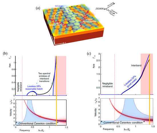
Figure 2. The sketch illustrates the 2D Cerenkov emission process in graphene. (a) GP emission from the graphene layer by the inner flow of hot carrier, diagram demonstrating the GP emission-related process due to the hot carrier in the graphene layer. (b, (c) illustrates the spectrum of the CˇE GP emissions, the red region corresponds to the GP losses and emission losses presented in black, where emission approximation is depicted with blue. The orange line shows the spectral cut off because of the Fermi sea, where all available states are filled. In the lower part of (b) and (c), the red curve depicts the GP related phase velocity, and its thickness corresponds to the GP losses [54].

Personal information: Muhammad Junaid is research scholar, At UTP PETRONAS, Malaysia and also permanent faculty member at BUITEMS, Quetta, Pakistan. Currently working on " The Design and Fabrication of Graphene-based Light Emitting Hetero Structure Device". The evidence of emission radiation from graphene make it a promising material for the future generation of optical devices to produce a thin, flexible, and lightweight optoelectronics device. Graphene light emitters may open the door to the development of mid-infrared to far-infrared light sources for gas sensing and infrared photodetection. The light emission radiations from graphene structures are explained in various theoretical aspects, including thermal emission, plasmons assisted emission, and electroluminescence, and have been extensively discussed. 

References

  1. Pareek, A.; Mohan, S.V. Graphene and its applications in microbial electrochemical technology. In Microbial Electrochemical Technology; Elsevier: London, UK, 2018; pp. 75–97.
  2. Yun, F.F.; Cortie, D.L.; Wang, X.L. Tuning the electronic structure in stanene/graphene bilayers using strain and gas adsorption. Phys. Chem. Chem. Phys. 2017, 19, 25574–25581.
  3. Papageorgiou, D.G.; Kinloch, I.A.; Young, R.J. Mechanical properties of graphene and graphene-based nanocomposites. Prog. Mater. Sci. 2017, 90, 75–127.
  4. Bao, W. Electrical and Mechanical Properties of Graphene. Ph.D. Thesis, University of California Riverside, Riverside, CA, USA, March 2012.
  5. Ramos Ferrer, P.; Mace, A.; Thomas, S.N.; Jeon, J.-W. Nanostructured porous graphene and its composites for energy storage applications. Nano Converg. 2017, 4, 29.
  6. Alvarado, Y.E.A.; de la Cruz, M.T.R.; Hernández-Cocoletzi, H.; Cocoletzi, G.H. Graphene structures: From preparations to applications. Handb. Graphene 2019, 1, 323–357.
  7. Lee, H.C.; Liu, W.-W.; Chai, S.-P.; Mohamed, A.R.; Aziz, A.; Khe, C.-S.; Hidayah, N.M.S.; Hashim, U. Review of the synthesis, transfer, characterization and growth mechanisms of single and multilayer graphene. RSC Adv. 2017, 7, 15644–15693.
  8. Alexeev, E.M.; Catanzaro, A.; Skrypka, O.V.; Nayak, P.K.; Ahn, S.; Pak, S.; Lee, J.; Sohn, J.I.; Novoselov, K.S.; Shin, H.S.; et al. Imaging of interlayer coupling in van der waals heterostructures using a bright-field optical microscope. Nano Lett. 2017, 17, 5342–5349.
  9. Rosli, N.N.; Ibrahim, M.A.; Ahmad Ludin, N.; Mat Teridi, M.A.; Sopian, K. A review of graphene based transparent conducting films for use in solar photovoltaic applications. Renew. Sustain. Energy Rev. 2019, 99, 83–99.
  10. Das, T.; Sharma, B.K.; Katiyar, A.K.; Ahn, J.H. Graphene-based flexible and wearable electronics. J. Semicond. 2018, 39, 011007.
  11. Romagnoli, M.; Sorianello, V.; Midrio, M.; Koppens, F.H.L.; Huyghebaert, C.; Neumaier, D.; Galli, P.; Templ, W.; D’Errico, A.; Ferrari, A.C. Graphene-based integrated photonics for next-generation datacom and telecom. Nat. Rev. Mater. 2018, 3, 392–414.
  12. Kusmartsev, F.V.; Wu, W.M.; Pierpoint, M.P.; Yung, K.C. Application of Graphene within Optoelectronic Devices and Transistors, In Applied Spectroscopy and the Science of Nanomaterials; Springer: Gateway East, Singapore, 2015; pp. 191–221.
  13. Sahu, S.; Rout, G.C. Band gap opening in graphene: A short theoretical study. Int. Nano Lett. 2017, 7, 81–89.
  14. Junaid, M.; Witjaksono, G. Analysis of band gap in AA and Ab stacked bilayer graphene by Hamiltonian tight binding method. In Proceedings of the 2019 IEEE International Conference on Sensors and Nanotechnology, Penang Island, Malaysia, 24–25 July 2019; pp. 1–4.
  15. Witjaksono, G.; Junaid, M. Analysis of Tunable Energy Band Gap of Graphene Layer. In Proceedings of the 2018 IEEE 7th International Conference on Photonics (ICP), Langkawi, Malaysia, 9–11 April 2018.
  16. Koppens, F.H.L.; Chang, D.E.; García De Abajo, F.J. Graphene plasmonics: A platform for strong light-matter interactions. Nano Lett. 2011, 11, 3370–3377.
  17. Cao, L.; Meziani, M.J.; Sahu, S.; Sun, Y.P. Photoluminescence properties of graphene versus other carbon nanomaterials. Acc. Chem. Res. 2013, 46, 171–182.
  18. Viskadouros, G.; Konios, D.; Kymakis, E.; Stratakis, E. Electron field emission from graphene oxide wrinkles. RSC Adv. 2016, 6, 2768–2773.
  19. Nguyen, B.H.; Nguyen, V.H. Advances in graphene-based optoelectronics, plasmonics and photonics. Adv. Nat. Sci. Nanosci. Nanotechnol. 2016, 7, 013002.
  20. Steranka, F.M.; Bhat, J.; Collins, D.; Cook, L.; Craford, M.G.; Fletcher, R.; Gardner, N.; Grillot, P.; Goetz, W.; Keuper, M.; et al. High power LEDs-technology status and market applications. Phys. Status Solidi Appl. Res. 2002, 194, 380–388.
  21. Gan, S.; Zhang, Y.; Bao, Q. Graphene Photonics, Optoelectronics, and Plasmonics; Pan Standford: Temasek Boulevard, Singapore, 2017; ISBN 9781315196671.
  22. Krames, M.R.; Shchekin, O.B.; Mueller-Mach, R.; Mueller, G.O.; Zhou, L.; Harbers, G.; Craford, M.G. Status and future of high-power light-emitting diodes for solid-state lighting. Ieee/Osa J. Disp. Technol. 2007, 3, 160–175.
  23. Chang, M.H.; Das, D.; Varde, P.V.; Pecht, M. Light emitting diodes reliability review. Microelectron. Reliab. 2012, 52, 762–782.
  24. Tak, Y.H.; Kim, K.B.; Park, H.G.; Lee, K.H.; Lee, J.R. Criteria for ITO (indium-tin-oxide) thin film as the bottom electrode of an organic light emitting diode. Thin Solid Film. 2002, 411, 12–16.
  25. Jiang, G.; Tian, H.; Wang, X.F.; Hirtz, T.; Wu, F.; Qiao, Y.C.; Gou, G.Y.; Wei, Y.H.; Yang, J.M.; Yang, S.; et al. An efficient flexible graphene-based light-emitting device. Nanoscale Adv. 2019, 1, 4745–4754.
  26. Kumar, P.; Woon, K.L.; Wong, W.S.; Mohamed Saheed, M.S.; Burhanudin, Z.A. Hybrid film of single-layer graphene and carbon nanotube as transparent conductive electrode for organic light emitting diode. Synth. Met. 2019, 257.
  27. Chae, M.S.; Lee, T.H.; Son, K.R.; Kim, Y.W.; Hwang, K.S.; Kim, T.G. Electrically-doped CVD-graphene transparent electrodes: Application in 365 nm light-emitting diodes. Nanoscale Horiz. 2019, 4, 610–618.
  28. Huang, Y.; Huang, Z.; Zhong, Z.; Yang, X.; Hong, Q.; Wang, H.; Huang, S.; Gao, N.; Chen, X.; Cai, D.; et al. Highly transparent light emitting diodes on graphene encapsulated Cu nanowires network. Sci. Rep. 2018, 8, 1–11.
  29. Woo, Y.S. Transparent conductive electrodes based on graphene-related materials. Micromachines 2018, 10, 13.
  30. Min, J.-H.; Son, M.; Bae, S.-Y.; Lee, J.-Y.; Yun, J.; Maeng, M.-J.; Kwon, D.-G.; Park, Y.; Shim, J.-I.; Ham, M.-H.; et al. Graphene interlayer for current spreading enhancement by engineering of barrier height in GaN-based light-emitting diodes. Opt. Express 2014, 22, 1040–1050.
  31. Park, P.S.; Reddy, K.M.; Nath, D.N.; Yang, Z.; Padture, N.P.; Rajan, S. Ohmic contact formation between metal and AlGaN/GaN heterostructure via graphene insertion. Appl. Phys. Lett. 2013, 102, 153501.
  32. Kim, Y.D.; Kim, H.; Cho, Y.; Ryoo, J.H.; Park, C.H.; Kim, P.; Kim, Y.S.; Lee, S.; Li, Y.; Park, S.N. Bright visible light emission from graphene. Nat. Nanotechnol. 2015, 10, 1–7.
  33. Ghosh, T.; Prasad, E. White-light emission from unmodified graphene oxide quantum dots. J. Phys. Chem. C 2015, 119, 2733–2742.
  34. Soavi, G.; Dal Conte, S.; Manzoni, C.; Viola, D.; Narita, A.; Hu, Y.; Feng, X.; Hohenester, U.; Molinari, E.; Prezzi, D.; et al. Exciton-exciton annihilation and biexciton stimulated emission in graphene nanoribbons. Nat. Commun. 2016, 7, 11010.
  35. Kim, D.H.; Kim, T.W. Ultrahigh-luminosity white-light-emitting devices based on edge functionalized graphene quantum dots. Nano Energy 2018, 51, 199–205.
  36. Jinyang, Z.; Xue, B.; Jialin, B.; Gencai, P.; Yongsheng, Z.; Yue, Z.; He, S.; Xu, C.; Biao, D.; Hanzhuang, Z.; et al. Emitting color tunable carbon dots by adjusting solvent towards lightemitting devices. Nanotechnology 2018, 29, 085705.
  37. Gao, Y.; Hou, F.; Hu, S.; Wu, B.; Wang, Y.; Zhang, H.; Jiang, B.; Fu, H. Graphene quantum-dot-modified hexagonal tubular carbon nitride for visible-light photocatalytic hydrogen evolution. ChemCatChem 2018, 10, 1330–1335.
  38. Liu, Z.; Bushmaker, A.; Aykol, M.; Cronin, S.B. Thermal emission spectra from individual suspended carbon nanotubes. ACS Nano 2011, 5, 4634–4640.
  39. Fares, H.; Almokhtar, M. Quantum regime for dielectric Cherenkov radiation and graphene surface plasmons. Phys. Lett. Sect. A Gen. Solid State Phys. 2019, 383, 1005–1010.
  40. Wang, Z.G.; Chen, Y.F.; Li, P.J.; Hao, X.; Liu, J.B.; Huang, R.; Li, Y.R. Flexible graphene-based electroluminescent devices. ACS Nano 2011, 5, 7149–7154.
  41. Bogue, R. Graphene sensors: A review of recent developments. Sens. Rev. 2014, 34, 233–238.
  42. Zrazhevskiy, P.; Sena, M.; Gao, X. Designing multifunctional quantum dots for bioimaging, detection, and drug delivery. Chem. Soc. Rev. 2010, 39, 4326–4354.
  43. Kim, D.H.; Kim, T.W. Ultrahigh current efficiency of light-emitting devices based on octadecylamine-graphene quantum dots. Nano Energy 2017, 32, 441–447.
  44. Barnard, H.R.; Zossimova, E.; Mahlmeister, N.H.; Lawton, L.M.; Luxmoore, I.J.; Nash, G.R. Boron nitride encapsulated graphene infrared emitters. Appl. Phys. Lett. 2016, 108, 131110.
  45. Freitag, M.; Chiu, H.Y.; Steiner, M.; Perebeinos, V.; Avouris, P. Thermal infrared emission from biased graphene. Nat. Nanotechnol. 2010, 5, 497–501.
  46. Lawton, L.M.; Mahlmeister, N.H.; Luxmoore, I.J.; Nash, G.R. Prospective for graphene based thermal mid-infrared light emitting devices. Aip Adv. 2014, 4, 087139.
  47. Mirza, B.I.; Nash, G.R.; Smith, S.J.; Buckle, L.; Coomber, S.D.; Emeny, M.T.; Ashley, T. Recombination processes in midinfrared AlxIn1-xSb light-emitting diodes. J. Appl. Phys. 2008, 104, 063113.
  48. Buss, I.J.; Nash, G.R.; Rarity, J.G.; Cryan, M.J. Three-dimensional numerical modeling of emission from InSb light-emitting diodes with patterned surfaces. J. Opt. Soc. Am. B 2008, 25, 810.
  49. Tielrooij, K.J.; Orona, L.; Ferrier, A.; Badioli, M.; Navickaite, G.; Coop, S.; Nanot, S.; Kalinic, B.; Cesca, T.; Gaudreau, L.; et al. Electrical control of optical emitter relaxation pathways enabled by graphene. Nat. Phys. 2015, 11, 281–287.
  50. Mišković, Z.L.; Segui, S.; Gervasoni, J.L.; Arista, N.R. Energy losses and transition radiation produced by the interaction of charged particles with a graphene sheet. Phys. Rev. B 2016, 94, 125414.
  51. Ullah, Z.; Witjaksono, G.; Nawi, I.; Tansu, N.; Khattak, M.I.; Junaid, M. A review on the development of tunable graphene nanoantennas for terahertz optoelectronic and plasmonic applications. Sensors 2020, 20, 1401.
  52. Ullah, Z.; Nawi, I.; Witjaksono, G.; Tansu, N.; Khattak, M.I.; Junaid, M.; Siddiqui, M.A.; Magsi, S.A. Dynamic absorption enhancement and equivalent resonant circuit modeling of tunable graphene-metal hybrid antenna. Sensors 2020, 20, 3187.
  53. Jablan, M.; Buljan, H.; Soljačić, M. Plasmonics in graphene at infrared frequencies. Phys. Rev. B-Condens Matter Mater. Phys. 2009, 80, 245435.
  54. Kaminer, I.; Katan, Y.T.; Buljan, H.; Shen, Y.; Ilic, O.; Lopez, J.J.; Wong, L.J.; Joannopoulos, J.D.; Soljacic, M. Efficient plasmonic emission by the quantum Č erenkov effect from hot carriers in graphene. Nat. Commun. 2016, 7, 11880.
  55. Hasan, M.T.; Senger, B.J.; Ryan, C.; Culp, M.; Gonzalez-Rodriguez, R.; Coffer, J.L.; Naumov, A.V. Optical band gap alteration of graphene oxide via ozone treatment. Sci. Rep. 2017, 7, 1–8.
  56. Essig, S.; Marquardt, C.W.; Vijayaraghavan, A.; Ganzhorn, M.; Dehm, S.; Hennrich, F.; Ou, F.; Green, A.A.; Sciascia, C.; Bonaccorso, F.; et al. Phonon-assisted electroluminescence from metallic carbon nanotubes and graphene. Nano Lett. 2010, 10, 1589–1594.
  57. Beams, R.; Bharadwaj, P.; Novotny, L. Electroluminescence from graphene excited by electron tunneling. Nanotechnology 2014, 25, 055206.
  58. Fei, Z.; Rodin, A.S.; Andreev, G.O.; Bao, W.; McLeod, A.S.; Wagner, M.; Zhang, L.M.; Zhao, Z.; Thiemens, M.; Dominguez, G.; et al. Gate-tuning of graphene plasmons revealed by infrared nano-imaging. Nature 2012, 486, 82–85.
  59. Kim, Y.D.; Bae, M.-H. Light emission from graphene. In Advances in Carbon Nanostructures; InTech: London, UK, 2016; pp. 83–100.
  60. Li, Y.T.; Tian, Y.; Sun, M.X.; Tu, T.; Ju, Z.Y.; Gou, G.Y.; Zhao, Y.F.; Yan, Z.Y.; Wu, F.; Xie, D.; et al. Graphene-based devices for thermal energy conversion and utilization. Adv. Funct. Mater. 2020, 30, 1903888.
  61. Miyoshi, Y.; Fukazawa, Y.; Amasaka, Y.; Reckmann, R.; Yokoi, T.; Ishida, K.; Kawahara, K.; Ago, H.; Maki, H. High-speed and on-chip graphene blackbody emitters for optical communications by remote heat transfer. Nat. Commun. 2018, 9, 1279.
  62. Wang, X.; Tian, H.; Mohammad, M.A.; Li, C.; Wu, C.; Yang, Y.; Ren, T.L. A spectrally tunable all-graphene-based flexible field-effect light-emitting device. Nat. Commun. 2015, 6, 7767.
  63. Adamo, G.; MacDonald, K.F.; Fu, Y.H.; Wang, C.M.; Tsai, D.P.; García De Abajo, F.J.; Zheludev, N.I. Light well: A tunable free-electron light source on a chip. Phys. Rev. Lett. 2009, 103, 113901.
  64. Fang, Y.; Sun, M. Nanoplasmonic waveguides: Towards applications in integrated nanophotonic circuits. Light Sci. Appl. 2015, 4, 294.
  65. Zhang, Q.; Li, X.; Hossain, M.M.; Xue, Y.; Zhang, J.; Song, J.; Liu, J.; Turner, M.D.; Fan, S.; Bao, Q.; et al. Graphene surface plasmons at the near-infrared optical regime. Sci. Rep. 2014, 4, 6559.
  66. Yu, H.; Peng, Y.; Yang, Y.; Li, Z.Y. Plasmon-enhanced light–matter interactions and applications. npj Comput. Mater. 2019, 5, 45.
  67. Yan, H.; Low, T.; Zhu, W.; Wu, Y.; Freitag, M.; Li, X.; Guinea, F.; Avouris, P.; Xia, F. Damping pathways of mid-infrared plasmons in graphene nanostructures. Nat. Photonics 2013, 7, 394–399.
  68. Alonso-González, P.; Nikitin, A.Y.; Golmar, F.; Centeno, A.; Pesquera, A.; Vélez, S.; Chen, J.; Navickaite, G.; Koppens, F.; Zurutuza, A.; et al. Controlling graphene plasmons with resonant metal antennas and spatial conductivity patterns. Science 2014, 344, 1369–1373.
  69. Lukianova-Hleb, E.Y.; Ren, X.; Sawant, R.R.; Wu, X.; Torchilin, V.P.; Lapotko, D.O. On-demand intracellular amplification of chemoradiation with cancer-specific plasmonic nanobubbles. Nat. Med. 2014, 20, 778–784.
  70. Geim, A.K. Graphene: Status and prospects. Science 2009, 324, 1530–1534.
  71. Wong, L.J.; Kaminer, I.; Ilic, O.; Joannopoulos, J.D.; Soljačić, M. Towards graphene plasmon-based free-electron infrared to X-ray sources. Nat. Photonics 2016, 10, 46–52.
  72. Silveirinha, M. A low-energy Cherenkov glow. Nat. Photonics 2017, 11, 269–271.
  73. Zhang, J.; Chen, P.; Yuan, B.; Ji, W.; Cheng, Z.; Qiu, X. One-dimensional electrical contact to a two-dimensional material. Science 2013, 342, 614–617.
  74. Jablan, M.; Soljačić, M.; Buljan, H. Plasmons in graphene: Fundamental properties and potential applications. Proc. IEEE 2013, 101, 1689–1704.
  75. Park, M.T. Graphene plasmonics: Challenges and opportunities. ACS Photonics 2014, 1, 135–152.
  76. Rana, F.; Strait, J.H.; Wang, H.; Manolatou, C. Ultrafast carrier recombination and generation rates for plasmon emission and absorption in graphene. Phys. Rev. B-Condens. Matter Mater. Phys. 2011, 84, 045437.
  77. Jariwala, D.; Marks, T.J.; Hersam, M.C.; Lee, C.H.; Lee, G.H.; Van Der Zande, A.M.; Chen, W.; Li, Y.; Han, M.; Cui, X.; et al. Light-emitting diodes by band-structure engineering in van der Waals heterostructures. Nat. Mater. 2016, 1, 952–958.
  78. Song, S.M.; Bong, J.H.; Hwang, W.S.; Cho, B.J. Improved drain current saturation and voltage gain in graphene-on-silicon field effect transistors. Sci. Rep. 2016, 6, 25392.
  79. Shiue, R.J.; Gao, Y.; Tan, C.; Peng, C.; Zheng, J.; Efetov, D.K.; Kim, Y.D.; Hone, J.; Englund, D. Thermal radiation control from hot graphene electrons coupled to a photonic crystal nanocavity. Nat. Commun. 2019, 10, 109.
  80. Soavi, G.; Wang, G.; Rostami, H.; Purdie, D.G.; De Fazio, D.; Ma, T.; Luo, B.; Wang, J.; Ott, A.K.; Yoon, D.; et al. Broadband, electrically tunable third-harmonic generation in graphene. Nat. Nanotechnol. 2018, 13, 583–588.
  81. Ginzburg, V.L. Quantum theory of radiation of electron uniformly moving in medium. Zh. Eksp. Teor. Fiz. 1940, 10, 589.
  82. Kaminer, I.; Mutzafi, M.; Levy, A.; Harari, G.; Sheinfux, H.H.; Skirlo, S.; Nemirovsky, J.; Joannopoulos, J.D.; Segev, M.; Soljacic, M. Quantum Čerenkov radiation: Spectral cutoffs and the role of spin and orbital angular momentum. Phys. Rev. X 2016, 6, 11006.
  83. Zhou, G.Y.; Ma, X.M.; Zhu, M.J.; Zhu, Z.H.; Tan, Z.L.; Qin, S.Q.; Liu, K. Ultrafast photoluminescence from suspended gold/graphene hybrid structures. J. Phys. Chem. C 2019, 123, 21265–21270.
  84. Yamoah, M.A.; Yang, W.; Pop, E.; Goldhaber-Gordon, D. High-velocity saturation in graphene encapsulated by hexagonal boron nitride. ACS Nano 2017, 11, 9914–9919.
  85. Yamoah, M.A.; Yang, W.; Pop, E.; Goldhaber-Gordon, D. High-velocity saturation in graphene encapsulated by hexagonal boron nitride. ACS Nano 2017, 11, 9914–9919.
More
Information
Contributors MDPI registered users' name will be linked to their SciProfiles pages. To register with us, please refer to https://encyclopedia.pub/register : , , , , , , , , ,
View Times: 863
Revisions: 3 times (View History)
Update Date: 21 Oct 2020
1000/1000