1000/1000
Hot
Most Recent
 +1 point
MoS2 belongs to a class of transition metal dichalcogenides (TMDCs). TMDCs share a common formula MeX2, where Me is a transition metal element from group four (Ti, Zr, Hf), five (V, Nb or Ta) or six (Mo, W), and X is a chalcogen (S, Se or Te). Their crystalline structure comprises an inner Me layer sandwiched by two X layers. Herein, thermal oxidation of the microscopic MoS2 flakes is reviewed. An impact of relative humidity is also mentioned.
Initially, microscopic and naturally occurring MoS2 crystals, aka molybdenites, were used as solid lubricants in various encapsulated devices, such as low Earth orbit (LEO) satellites [1]. This is thanks to their low friction and propensity to peel off easily, because of any two adjacent layers interacting weakly via the van der Waals forces [2][3][4]. Later in time, microscopic MoS2 crystallites and their composites found usage in batteries, photovoltaic devices and catalysts for the hydrogen evolution reaction (HER) and other catalytic processes [5][6][7][8][9]. In recent years, interest in single MoS2 crystals has surged in the context of nanoelectronics, particularly on flexible substrates. According to the Web of Science, a number of published papers with the “MoS2” keyword increased slowly from 164 papers in 2000 to 220 papers in 2010, but then it started to grow exponentially from 288 papers in 2011 to reach 5549 papers in 2019 and level off to 5661 manuscripts published in 2020. Coincidently, year 2011 marked appearance of the first published reports about single-layer MoS transistors [10].
Most of the current research with MoS2 crystals has been performed on the 2H MoS2 polymorph. Moreover, 2H MoS2 has been shown to be a 2D semiconductor with high electron mobilities of up to 200 cm^{2} V^{−1} s^{−1} and a bulk 1.2 eV indirect bandgap, which increases and changes its character with decreasing number of the MoS2 layers, so that the 2H MoS 2 monolayer has a 1.8 eV direct bandgap [2]. These properties make single 2H MoS 2 flakes of variable thickness an ideal material for tightly packed nanoscale transistors and devices with variable bandgap. Recently, single-layer MoS2 based transistors, as well as their assemblies in the form of logic circuits[11][12][13] and in-memory computing devices with room-temperature current on/off ratios of 1 × 10 8 and ultralow standby power dissipation in single layers of MoS2, have been developed [14][15]. At the same time, great progress has been made into synthesis of wafer-scale polycrystalline MoS2 monolayers[16] and large-domain single-crystalline MoS2 monolayers by chemical vapor deposition [13][17], as well as the wafer-scale transfer and stacking of monolayer MoS2 for heterogeneous integrations [18][19]. Due to discovery of large photoluminescence quantum efficiency of the chemically treated MoS2 crystals [20], next-generation flexible nanoelectronics devices based on single MoS2 flakes appear already in sensing, optoelectronics and energy harvesting [2][21][22]. Furthermore, the presence of various conduction mechanisms beyond electronic currents, such as spin currents, polariton currents, valley and other topological currents within single MoS2 layers and/or their heterostructures with other 2D materials, has opened new vistas in the MoS2 based nanoelectronics[2][23][24].
Each microelectronic device heats up while working, mostly due to Joule heating, and some MoS2 based transistors have been measured recently to locally reach 250 °C and more [25]. In addition, exposure to ambient conditions has been shown to reversibly reduce the on-state current in back-gated bilayer MoS2 based FETs by up to two orders of magnitude [26]. However, other studies on thin MoS2 FET transistors have shown up to three-fold drops in carrier mobilities in air with respect to vacuum, which did not recover upon vacuum annealing[27]. Therefore, it is important to investigate the chemical surface reactivity of single MoS2 flakes in ambient conditions above room temperature. Furthermore, the impact of relative humidity cannot be neglected due to capillary condensation at local lengths[28][29].
From the time of seminal works of Ross et al. [30] on Mo polycrystalline powders in the 1950s till about the 2010s MoS crystals have been considered inert to oxidation till 600 °C in air [31]. Substantial progress has been made in this field, particularly after 2013, when several seminal papers about local oxidative etching have been published[32][33][34]. A whole zoo of the surface reactions of 2H MoS2 crystals with oxygen, much beyond oxidative etching, has been discovered by using high-resolution tools, such as AFMs, SEMs and TEMs. These reactions involve physio and chemical oxygen adsorption, oxygen dissociative reactions, and other direct and non-direct oxidation mechanisms, as well as oxygen penetration between the stacked MoS2 layers [32][33][34][35][36][37][38][39][40][41][42]. Below, we present a brief survey of the results obtained on various MoS2 as a function of temperature and relative humidity. Despite substantial efforts interactions of oxygen with single MoS2 flakes and crystals are still not completely understood, particularly in terms of competing thermal etching mechanisms.
To start with, one must acknowledge major differences between MoS2 powders, bulk MoS2 crystals and single MoS2 flakes. Pulverized MoS2 powders comprise mostly the 2H MoS2 polymorph, and their physicochemical properties have been studied macroscopically. Bulk MoS2 crystals have been studied on the macro- and micro-scales, but mostly computationally. Single microscopic and exclusively 2H MoS2 crystalline flakes of various thickness from one monolayer (ML) to much thicker structures have been studied computationally, as well as experimentally. Research in these different MoS2 forms and such different length scales have provided certain amount of information at each length scale, which is often not directly transferable to a different length scale.
Early experimental studies of polycrystalline MoS2 powders have shown that Mo oxide layers present on the surface form slowly and act as passivating layers till at least 100 °C [30][34]. The appearance of Mo oxides at room temperature, mostly in the form of MoO3 (with other oxide forms below a detection threshold), has been confirmed as well on the CVD-grown defective MoS2 monolayers[43]. However, in contrast to the MoS2 powders and CVD-grown MoS2 samples, freshly exfoliated single MoS2 flakes did not show any direct manifestations of the protective oxide layers [44]. The lack of the passivating Mo oxide layers on single mechanically exfoliated MoS2 flakes has been confirmed even in the samples left in air for a year. Single MoS2 flakes, however, have been shown to gradually increase their number of sulfur defects when left in air, which, in turn, became oxidized towards substitutional Mo species, but not MoO3[45]. Nevertheless, some variations in the MoS2 stoichiometry between even the same kind of mechanically exfoliated samples also take their toll and produce detectable differences across the same samples [46].
As the temperature has been increased, Yamamoto et al. [34] showed—via local micro-Raman studies—that thin MoS2 flakes start to show any electronic density changes above 200 °C. In the light of the aforementioned studies, this might mean that accumulation of defects and oxygenated S vacancies start to become detectable microscopically only above 200 °C. At temperatures between 320 and 400 °C oxidative thermal etching regime has been observed in the case of single MoS2 flakes [32][33][34][39]. Such conditions have produced characteristic microscopic triangular etch pits within the MoS2 basal planes, as has been observed mostly via AFM. The etch pits were typically only 1 ML deep and have been observed on thin and thick single MoS2 flakes. Furthermore, they changed orientations in between the subsequent layers, which has been explained based on the crystal structure of the 2H MoS2 polymorph [39]. When single MoS2 crystals were heated for a short time, the etch pits on basal planes were associated with virtually no change in thickness and lateral dimension of the studied MoS2 crystals. Variability of the growth speeds for the triangular etch pits has been observed between MoS2 flakes, which suggested thermally activated processes being at the origin of oxidative etching[34][39]. Ukegbu et al. have exploited this observation further to calculate activation energy of the oxidative etching process from the growth rate of the triangular etch pits[39] . The triangular shape of the pits was related to the hexagonal symmetry of the Mo planes within the MoS2 crystal lattice, and several mechanisms for their creation have been proposed[32][34][39][47]. Thanks to the S-TEM studies, a zigzag Mo (ZZ-Mo) edge was assigned as the dominant termination of the triangular etch pits [47]. Further details on triangular etch pits formation have been found using local Raman studies of the signature MoS2 Raman bands at 384 cm−1 (E12g mode) and 408 cm−1 (A1g mode). The observed results, particularly in the case of thin MoS2 flakes, pointed out an electron density withdrawal from the MoS2 layer and consequently its p-type doping upon progressive oxidative etching. In addition to etching two other kinds of interactions with molecular oxygen, which can also follow up oxidative etching, have been observed. In particular, the presence of small MoOx clusters, identified as mostly the MoO3 clusters, as well as presence of small MoO3 patches [33][41]. Furthermore, other processes have been spotted, such as oxygen diffusion into the freshly exposed etch pits[48] and oxygen incorporation in between the MoS2 sheets, which based on the XRD results swells the MoS2 crystals.
Above 400–410 °C substantial oxidation involving decrease of the flakes’ volume has been observed in air [40][49]. It confirmed predictions about particularly fast oxidation along the crystalline edges[40][41][50][51] . Oxidation and oxidative etching in some instances produced visible MoO3 deposits (in various forms) appearing on the single MoS2 flakes/nanosheets [41][52][53] or even full MoS2 transformation [35] [34]into single MoO3 crystals. Oxidation at temperatures of more than 500 °C has been shown to be detrimental even to the thick MoS2 flakes and led to formation of deep indents and likely Mo oxide patches with messy topographies[40][49]. Those were surface morphologies without any clear pit pattern (observed previously in oxidative etching), but rather with many surface pits of various depths and various forms of surface islands with frayed edges. Often, some dendritic structures were observed. The resulting Mo oxides have been shown to leave the substrate surface, but often not entirely if oxidation was not too rapid[34][35][39] .
The aforementioned phenomenological aspects related to the MoOx formation on globally heated basal planes within the MoS2 flakes in dry air are summarized in Figure 1 below.
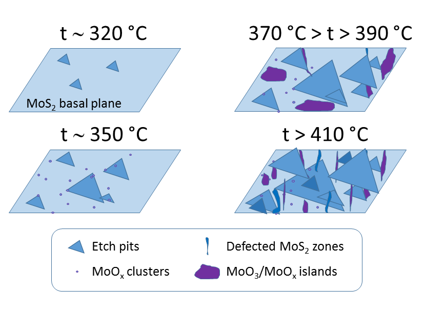 Figure 1. Phenomenological aspects of the MoOx formation onto MoS2 basal planes during their heating in dry air. Above ca. 320 °C, triangular 1 ML deep etch pits were observed[32][33][34][39] . Nucleated growth of the etch pits was supplemented by appearance of small sub-nm size MoOx clusters detected already at ca. 350 °C via a combination of various experimental techniques[52] . At temperatures between 370 and 390 °C, the largest amounts of Mo oxides and their derivatives accumulate on the MoS2 surface [41]. Some of it forms irregular patches (marked in violet)[33][41]. Above 410 °C, less oxide has been detected indirectly and locally via AFM techniques, as well as chemically and globally via XPS studies. In addition, in this regime, substantial surface defects have been observed.
In addition to the temperature related oxidation results in dry air, presented in Fig. 1, water vapors have been shown to change everything and produce larger amounts of Mo oxides and generally quicker basal plane passivation by complete and thin MoO3 layers then oxidation in air[30][35][41]. To complement the aforementioned findings, the studies in water at ambient conditions have provided the following conclusions. Defective MoS2 nanosheets have been found to partially dissolve in water, particularly above pH = 2 and at concentrations of total Mo of less than 2 mM[54]. Their dissolution products were various kinds of molybdate ions, with monomolybdates prevailing above pH of 6–8, depending on the report. Single non-defective MoS2 flakes have been found by some researchers to be stable in water, while other reports showed needlelike protrusions on MoS2 crystals left in water for more than 1 h. Thus, more research is needed to resolve this issue.
A great majority of mechanistic approaches used atomistic calculations based on the local DFT approaches, which were a primary tool for investigating defect formation energies, reaction energy barriers, reaction mechanisms and the electronic structure properties of the considered MoS2 atomistic structures.
Regarding engaging into a chemical reaction, the O2 molecules, in contrast to atomic oxygen, have been computationally shown to be non-reactive towards the S atoms. A high kinetic activation energy barrier of 1.59 eV was obtained for dissociative adsorption of the O2 molecule on 1 ML thick MoS2 . Dissociative oxygen adsorption leads to adsorbed oxygen atoms in the form of two stable oxygen-terminated sulfurs. Not only is the kinetic barrier for dissociative O2 adsorption large, but the process is thermodynamically not efficient, because its binding energy of about 0.8 eV is much less than the kinetic barrier of 1.59 eV [42][55]. Therefore, it is not expected to propagate, and single O2 dissociative events are rare.
The findings of Santosh et al. [42] contributed well to explaining the exceptional stability of the pristine, non-defective MoS2 flakes against oxidation. Direct oxygen binding to Mo atoms is impossible on pristine basal planes due to steric reasons. However, other oxidative processes have been found to exist on pristine and non-defective MoS2 basal planes. For example, oxygen-induced single sulfur vacancy (SSV) creation was observed by Peto et al. [56], who—due to advances in local scale imaging—supplemented their DFT calculations with experimental observations.
Recently, a more comprehensive scenario for initial events associated with oxidative etching has been proposed by Farigliano et al. [72][57] for the non-defective MoS2 basal plane. They used NEB calculations at 0 K temperature to find out crucial intermediates within the processes and then proceeded with ab initio molecular-dynamics simulations at higher temperatures to show decomposition pathways of the key intermediate in the processes. The key initial intermediate consisted of an O atom adsorbed on top of an S atom (Oads) with a second O atom inserted (Oin) into the S-Mo bond, i.e., the OSOMo moiety. Such an intermediate was obtained via two pathways. The first pathway proceeded via a dissociative oxygen adsorption pathway on neighboring sulfur atoms and its further surface reorganization. Second pathway was a direct O2 adsorption on the same sulfur atom and its further surface reorganization. However, calculated activation energies for both pathways are at least 0.4 eV more than obtained via Santosh et al. [42] for dissociative oxygen adsorption onto pristine MoS2, which suggests that the trajectory proposed by Farigliano et al. [57] is less probable or that there are differences in the DFT implementations between these studies. Nevertheless, the results of Farigliano et al. provide an important link between the dissociative oxygen adsorption and oxidative etching. This is because, in the subsequent steps, Farigliano et al. [57] have found out that the OSOMo intermediate decomposes either via direct SO2 desorption to generate a single sulfur vacancy, or via SO desorption, leaving substitutional oxygen on the surface.
It has been established that single sulfur vacancies in the basal sulfur planes are the most frequent and important from the point of view of an initial oxygen attack [58][59][60], since their activation energies are much less than in the case of non-defected basal planes. Along this line of research Martincová et al. have studied oxidative etching directly on “simplified edges” of the MoS2 crystals[50][61]. The initial state was taken to be the one in which the O2 molecule is in the edge vicinity. The final state of the dissociative splitting was taken to be the one with two separate oxygen atoms adsorbed on adjacent sulfur atoms at an edge. Several dissociation pathways were considered, differing mainly in an initial position of the O2 molecule. The most favorable pathway yielded a very low O2 dissociation barrier of only 0.31 eV and several other pathways yielded similar barriers, all not exceeding 0.5 eV. Such results still do not suggest immediate dissociative O2 splitting onto MoS2 edges; however, they clearly produce much lower Ea values than 0.8 eV obtained by Santosh et al. for the same process on a defective MoS2 basal plane. However, the link between dissociative oxygen adsorption and oxidative etching is not straightforward due to other various steps necessary.
Overall, there are several successes of the presented above theoretical approaches. First, chemical inertness for reactions with oxygen of the non-defective MoS2 basal planes at room temperature has been explained in terms of high activation barrier for a dissociative oxygen adsorption onto such planes with an energy barrier of at least 1.6 eV. Second, according to experimental results, oxygen-induced single sulfur vacancy (SSV) creation and its later oxidation have been shown to slowly introduce defects within the MoS2 flakes, even at room temperatures, thus making them prone to oxidation via decreasing the energy barrier down to 0.8 eV on SSV and to 0.3 eV on edges/grain boundaries. These results agree qualitatively with experimentally obtained activation energies for oxidative etching which range from 0.6 to ca. 1 eV for pristine MoS2 samples, where single oxidation events according to the transition state theory would occur on the time scales of months.
Last, but not least, a unified picture for oxidative etching is still elusive. Some models and theoretical simulations refer to dissociative oxygen adsorption on sulfur atoms as an initial limiting step, i.e., studies by Martincová et al. [62], as well as by Farigliano et al. [57], while others refer to direct reaction of oxygen with Mo atoms exposed due to omnipresent single sulfur vacancies, i.e., Lv et al.[58], Santosh et al. [42] and Zhou et al. [33][32]. In addition, the role of initially physically adsorbed oxygen in thermal etching is still not clear[40], since its diffusion to the reaction centers can compete with direct reactions with atmospheric oxygen.