In this review, previously presented RHBD FFs are classified into three categories with an overview of
each category. Six well-known RHBD FFs architectures are simulated using a 180 nm CMOS process
to show a fair comparison between them while the conventional Transmission Gate Flip-Flop (TGFF)
is used as a reference design for this comparison. The results of the comparison are analyzed to give
some important highlights about each design.
1. Introduction
When an energetic particle hits a logic circuit, it can introduce a temporary voltage disturbance due to charge depositing that can upset sensitive circuit nodes and propagate to the successive blocks
[1]. Electron-hole pairs are generated corresponding to the strike of an ionizing particle with the transistor nodes, resulting in a generated charge that depends on the Linear Energy Transfer (LET) of the striking particle. At a certain threshold, this charge becomes critical and causes a soft error that flips the logic output
[2]. These events are known as Single Event Transients (SETs), and they can be latched by registers causing an error in the stored bits, which is called Single Event Upsets (SEUs)
[1][2]. Mitigating SEU is crucial in space and nuclear applications due to the existence of higher energetic particles such as heavy ions and protons
[1][3]. Recently, SEU has become a terrestrial problem in modern nanoscale CMOS technology since a small amount of charge can upset the data stored in the Flip-Flops (FFs)
[4].
Two techniques can be implemented in the device level of the FF to increase its immunity to SEU that are Radiation-Hardened-by-Process (RHBP) and Radiation-Hardened-by-Design (RHBD)
[5]. The first technique is executed at the fabrication process of the CMOS transistors by modifying their geometrical parameters. The other technique concerns the FF architecture such as redundancy and filtering. It is independent of the technology size but results in some overhead in area, power, delay, or cost.
RHBD FFs, in this review, are classified into three different categories; they are spatial redundancy FF that makes different copies of the same FF in space
[1][6][7][8][9], temporal redundancy FF that compares the signal at different times by adding some delay
[10][11][12][13][14], and node hardening FF that strengthens the internal nodes of the FFs and protects them from flipping by soft errors
[4][15][16][17][18][19][20][21][22]. Additionally, some FFs can be categorized into multiple categories such as spatial–temporal redundancy FF
[7][23][24][25][26] or node hardening FF with spatial/temporal redundancy
[27][28].
2. Conventional Transmission Gate Flip-Flop (TGFF)
Conventional TGFF is a well-known FF topology that is used in many earlier microprocessors and it is a modified version of the popular FF used in the PowerPC 603 processor (NXP Semiconductors, Eindhoven, Netherlands)
[29][30][31].
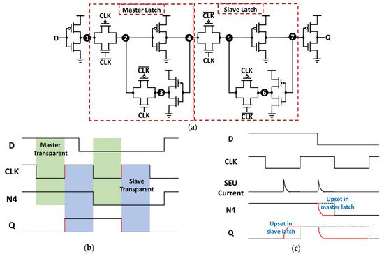
Figure 1a shows the circuit diagram of TGFF, which consists of a master latch that captures the input D signal when the CLK is low and keeps it when the CLK is high; and a slave latch that operates on the opposite CLK levels as the signal is passed from master latch to slave latch while the CLK is high, and it is kept as long as the CLK is low. Accordingly, the signal has to pass through the master latch during the CLK = 0 and pass through the slave latch during the CLK = 1, which means that the input signal D is only transferred to the output Q when the CLK changes from 0 to 1 (Positive edge of the CLK) as illustrated in
Figure 1b.
Figure 1. Conventional Transmission Gate Flip-Flop (TGFF): (a) TGFF circuit diagram consisting of master and slave latches; (b) Waveforms showing the operation of TGFF; (c) Effect of Single Event Upset (SEU) on TGFF on both master and slave latches.
Conventional TGFF has a relatively small area and is one of the most power-efficient topologies compared to other master–slave latch-pairs
[31], which makes it a good candidate to be used as a benchmark to compare other FFs. However, TGFF is weaker against soft errors by order of ~2× or ~3× than other RHBD FF
[32]. The master latch of TGFF can be easily upset by the soft errors that happen when the CLK is high (in the hold state of the master latch) while the slave latch can be upset when the CLK is low (in the hold state of the slave latch) as shown in
Figure 1c. Additionally, soft errors can affect TGFF during the transparent state if this error is propagated and latched by the next latch
[6].
3. Radiation-Hardened-by-Design Flip-Flops (RHBD FF)
There are numerous designs for RHBD FF. In this review, we divide them into three main categories, which are spatial redundancy, temporal redundancy, and nodes hardened.
3.1. Spatial Redundancy FF
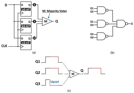
SEU is collected by a single node at a certain time. Spatial redundancy FF designs make replicas of each logic and check their outputs to detect the error or correct it
[6]. XOR gate can be used to compare the output of two redundant FFs and produces an error signal if they do not match. To determine the correct output, a third FF is required, and a majority voter circuit is connected to the output of the three FFs. This design is considered one of the most popular RHBD FFs, which is well-known as Triple Modular Redundancy (TMR) FF, and it is illustrated in
Figure 2a
[1][7]. TMR FF is very immune to soft errors, but it requires a 3× larger area than the conventional TGFF, and thus exhibiting 3× power consumption overhead.
Figure 2. Triple modular redundancy Flip-Flop (TMR FF) votes between three copies of FFs with the same data: (a) Circuit diagram of TMR; (b) Majority voter circuit; (c) The outputs of the three copies are voted to give the final correct output.
TMR stills can fail to SEU in advanced nanoscale technologies due to charge sharing accompanied by the decreased distance between transistors
[6]. However, the charge sharing effect can be reduced by proper layout techniques.
The majority voter circuit, shown in
Figure 2b, simply consists of two-level NAND gates that generate an output that agrees with any two consistent inputs. If only one FF is upset, the majority voter ignores it and keeps the correct output relying on the other two correct FFs as demonstrated in
Figure 2c. Since the voter is connected to the output of the three replicas, if the particle hits the voter circuit with enough charge, it can flip the final output
[6]. However, this fault is instantaneous and it is not latched.
3.2. Temporal Redundancy FF
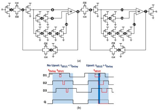
Another technique that can help in countering soft errors is to make delayed replicas at different times of the same signal and vote between them as shown in
Figure 3a. This makes the FF resists the SEU effect as long as the delay time is larger than the SEU current period.
Figure 3b. shows how the delay time can affect the resilience of the FF to the soft error
[10]. On the left side of the figure, the soft error time is less than the delay time which makes the disturbance takes effect at a different time, and at any certain moment, the majority voter circuit sees at least two correct inputs. Accordingly, the FF can tolerate the error by voting between three signals easily. On the other hand, if the soft error time exceeds the delay time, two signals would suffer from disturbance at the same time resulting in a fault at the final output. One major disadvantage of the added delay elements is reducing the maximum allowable frequency that the temporal redundancy FF can operate at. This is because the signal path with the longest delay elements would significantly increase the CLK to Q delay of the FF, which makes it unsuitable for high-speed applications.
Figure 3. Temporal redundancy FF uses delay elements to get the signal at different times: (a) Circuit diagram of a simple temporal redundancy FF; (b) The output signal shows how the delay time can tolerate the soft error.
3.3. Node Hardened FF
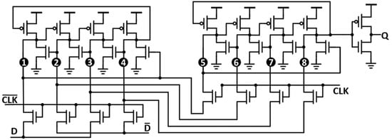
This category comprises any design technique that relies on protecting or hardening the internal nodes of the FF and makes them difficult to flip by soft errors. Dual Interlocked storage Cell (DICE) FF, shown in Figure 4, is one of the most common techniques in this category.
Figure 4. Circuit diagram Dual Interlocked storage Cell (DICE) FF. Two nodes 1 and 3 (or 2 and 4) have to be flipped simultaneously to overwrite the FF stored value.
The logic states of any node in the DICE latch are controlled by two adjacent nodes, so the DICE latch requires two simultaneous nodes with the same logic to be flipped to change its state, while the soft error that hits only one node at a time will be tolerated
[15]. DICE is classified here as a node hardened FF; however, it can also be classified as a spatial redundancy FF
[4]. There is another node hardened latch that has four storage nodes as a DICE latch, Quatro latch
[17].
Node hardening can also be obtained by using stacked inverters instead of standard inverters as it is stronger to soft errors
[18]. This method is immune to soft errors when it is used with Silicon on Thin Box (SOTB) process, which prevents the charge sharing effect because a BOX layer isolates transistor channels. Accordingly, the output of the stacked inverters flips only when both of its nMOS transistors are hit by energetic particles at the same time
[19]. One drawback of this method is the increased delay because of the duplicated gate capacitance and output resistance compared to conventional FF. In
[19][20] other FF designs using stacked transistors are implemented based on the adaptive coupling to reduce the power consumption and delay. A comparison between a stacked transmission-gate FF and a stacked tristate-inverter FF is presented in
[22] shows a similar strength to soft errors of both FFs, while stacked tristate-inverter FF has less delay by 21% with a larger area by 9% than the stacked transmission-gate FF.
The fourth structure for node hardening
[21] uses an RC filtering structure with an adaptive SEU detecting circuit to control the functions of the switches that automatically control the involved RC filtering structure in the sensitive nodes. This adaptivity makes the system able to select between higher speed or higher SEU immunity based on the detected values of the critical nodes.
3.4. Hybrid Hardened FF
The above three topologies can be combined to construct a hybrid topology.
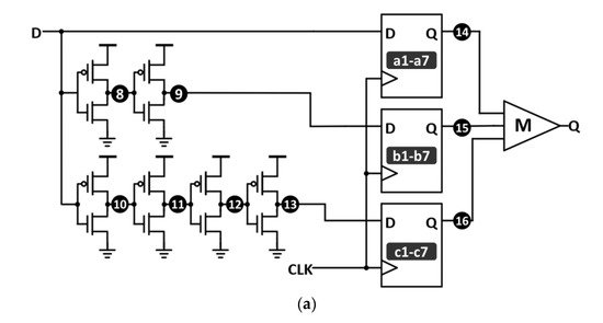
Figure 5a shows a combination of spatial–temporal redundancy FF that consists of TMR FF with delay elements
[7]. This temporal-TMR FF can possess a higher soft error immunity even with the charge sharing effect. On the other hand, it suffers from the same size problem of the TMR FF and the speed problem of temporal redundancy FF. Another spatial–temporal redundancy FF is known as Dual Modular Redundancy (DMR) FF, shown in
Figure 5b. It depends on two replicas of the conventional FF instead of three replicas as TMR
[23]. The outputs of the two copies are connected to a C-element. The truth table of the C-element is shown in
Table 1. The C-element delays the change in the final output until both copies of the FF agree together. Accordingly, even if one copy is upset, the final output keeps its previous state. A third spatial–temporal redundancy FF, radiation-hardened scan FF (RH-SFF)
[24], corrects soft errors in the sequential element and its preceding combinational logic.
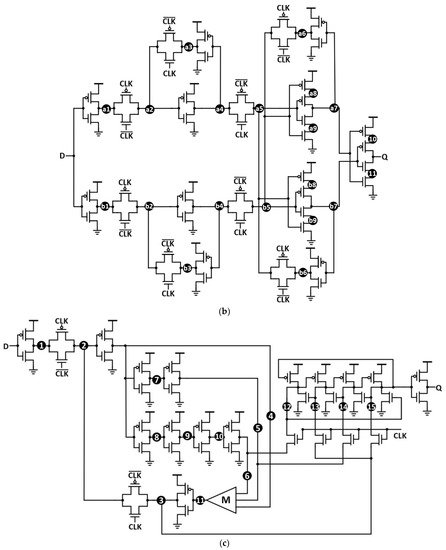
Figure 5. Hybrid FF topologies: (a) Circuit diagram of temporal-Triple modular redundancy (TMR) FF; (b) Circuit diagram of Dual Modular Redundancy (DMR) FF based on C-element; (c) Circuit diagram of temporal-DICE FF.
Table 1. Truth table of the C-element.
| A |
B |
Out |
| 0 |
0 |
0 |
| 0 |
1 |
Float |
| 1 |
0 |
Float |
| 1 |
1 |
1 |
One more hybrid topology is shown in
Figure 5c, which consists of a temporal master latch and a DICE slave latch
[27]. Similar to temporal-TMR FF, the temporal-DICE FF can get the hardening advantages of both DICE and temporal redundancy, but it also suffers from the disadvantages of speed limitations due to delay elements.
 +1 point