Light-emitting diodes (LEDs) based on Gallium Nitride (GaN) have been revolutionizing various applications in lighting, displays, biotechnology, and other fields. Many theoretical models have been developed for GaN-LED simulation, analysis, and design optimization, including carrier transport models, quantum well recombination models, and light extraction models. The overview below is a strongly abbreviated version of Ref. [1].
- LED
- GaN
- efficiency
- modeling
- simulation
1. Introduction
The promise of superior energy efficiency is the main driving force of many research activities on GaN-LEDs. However, high efficiency is only observed at low injection current density and low power (Figure 1). With rising current, injected electron–hole pairs disappear increasingly in parasitic processes without generating light, thereby causing severe efficiency droop. Still debated is the specific non-radiative mechanism that dominates this efficiency droop, which may be different in different devices. The two leading explanations are Auger recombination inside the light-generating InGaN quantum wells (QWs) and electron leakage into p-doped layers, respectively, in possible combination with other effects (see Figure 2 for illustration). However, very few direct measurements of either mechanism are published, none of which establishes a dominating magnitude. Most publications on efficiency droop mechanisms base their quantitative claims on modeling and simulation. Nevertheless, the total energy efficiency is usually of greater importance.
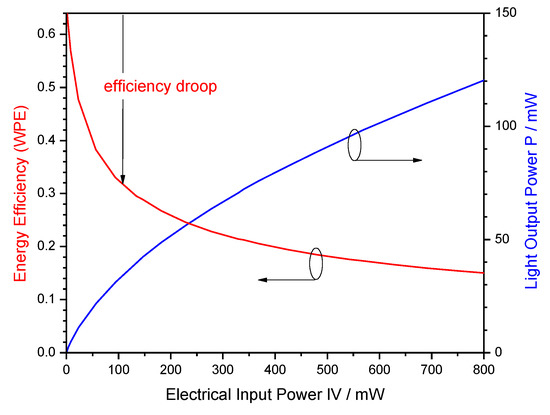
Figure 1. Illustration of the energy efficiency (wall-plug efficiency WPE) as ratio of output power to input power.
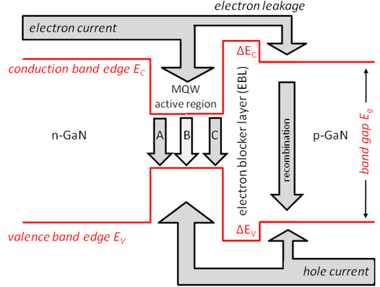
Figure 2. Illustration of the vertical LED energy band diagram including current flow and electron–hole recombination processes (A—defect-related recombination, B—photon emission, C—Auger recombination). Multiple quantum well (MQW) active regions typically consist of InGaN wells and GaN barriers. The electron blocker layer (EBL) is typically made of AlGaN.
The energy efficiency of the LED semiconductor chip is equivalent to the so-called wall-plug efficiency (WPE) which gives the ratio of light power P emitted from the chip to electrical power IV injected into the chip (I—injected electron–hole current, V—bias) as illustrated in Figure 1. Different energy loss mechanisms reduce the WPE, which are distinguished by splitting the WPE into separate components:
|
WPE = ELE × EQE = ELE × IQE × LEE = ELE × IE × RE × LEE |
(1) |
First, the injected electrons lose some energy on their way to the QWs, which is accounted for by the electrical efficiency ELE = hν/qV (hν—photon energy, q—electron charge). The remaining external quantum efficiency EQE = WPE/ELE is the ratio of emitted photon number to injected number of electron–hole pairs. The conversion of electron–hole pairs into emitted photons is accompanied by carrier losses and by photon losses: EQE = IQE × LEE. The light extraction efficiency LEE accounts for photon losses due to internal light reflection and absorption. The internal quantum efficiency IQE is the fraction of the total current that contributes to the desired photon generation inside the QWs. It can be further separated into the injection efficiency IE (current fraction that enters the QWs) and the radiative efficiency RE (fraction of QW carriers that recombines radiatively).
While WPE can be measured, the analysis of energy loss mechanisms depends mainly on modeling and simulation. For more than a decade, various models have been published for each GaN-LED efficiency component. These models can be separated into carrier transport models, QW recombination models, and light extraction models.
2. Carrier Transport Models
Drift-diffusion models based on the semiconductor transport equations are commonly employed for simulating the carrier movement of electrons and holes in GaN-LEDs. Carrier mobilities are crucial material properties in such models, besides recombination coefficients which are covered in the next section. Together with the free carrier density, the mobility determines the conductivity of each semiconductor layer. The low hole conductivity of Mg-doped III-nitride semiconductors typically dominates the LED bias. Due to the large Mg acceptor ionization energy, high Mg doping densities are required which in turn limit the free hole mobility by impurity scattering. Advanced models for carrier transport parameters have been developed; nevertheless, the material quality of fabricated devices is often best represented by experimental data, especially in the case of alloy layers.
Several groups employ Monte-Carlo transport models to track the path of individual carriers using tailored scattering models, partially in combination with drift-diffusion models. In particular, the movement of high-energy (hot) electrons has been investigated this way.
Quantum mechanical transport models based on the Non-Equilibrium Green’s Function (NEGF) method have been published more recently. Such models are especially valuable in the investigation of tunneling and carrier leakage processes. Simplified tunneling models have been implemented in drift-diffusion simulations to investigate multi-quantum barriers, trap-assisted interband tunneling, or LED structures with tunnel-junction cascaded active regions.
3. Quantum Well Carrier Recombination Models
Electrons and holes injected into the quantum wells of the LED can be consumed by different recombination mechanisms (cf. Figure 2):
-
Crystal defect related recombination
-
Radiative recombination
-
Auger recombination
Accordingly, the simple and popular ABC model adds up these different contributions to the total recombination rate R(n) = A·n + B·n2 + C·n3 (n—QW carrier density; A, B, C—material parameters) and the net current density injected into the QWs j(n) = q·d·R(n)·(d—total active layer thickness). The radiative efficiency is then given by
|
RE(n) = B·n 2 /(A·n + B·n 2 + C·n 3 ) |
(2) |
However, the actual QW carrier density n is typically unknown so that different ABC parameter sets lead to identical efficiency characteristics RE(j). In fact, the QW carrier density is known to be non-uniform across a multi-quantum well active region and may even vary inside each QW due to current crowding and/or QW non-uniformities. Various groups proposed modified ABC models, e.g., to account for a reduced active volume, inhomogeneous carrier distribution, electron leakage, photon quenching, multi-level defects, trap-assisted Auger recombination, built-in fields, or temperature effects. In any case, ABC models serve as an important bridge between experiment and theory. More detailed models for each of the recombination mechanisms are discussed in Reference [1][1].
4. Light Extraction Models
Photons generated spontaneously in the quantum wells travel in all directions inside the LED chip; however, only a fraction is able to escape from the chip, due to internal reflection and absorption. Ray tracing models are often employed to calculate LEE. However, ray optics fails when structures as small as the photon wavelength are involved. In such cases, Maxwell’s equations are usually solved employing the Finite-Difference Time-Domain (FDTD) method, in particular for nano-wire LEDs and photonic-crystal LEDs. Tailored models have been developed for textured LED surfaces and for the influence of Phosphor layers outside the semiconductor chip. Some models also include photon recycling, i.e., their re-absorption by the quantum wells. Light polarization effects need to be considered in deep ultraviolet AlGaN-based LEDs.
Please check the review paper below for more details and further references.
References
References
- Piprek, J. Efficiency Models for GaN-Based Light-Emitting Diodes: Status and Challenges. Materials 2020, 13, 5174.

