1000/1000
Hot
Most Recent
 +1 point
The diffusion of nitrogen into TiSi2 films of low electrical resistivity, deposited on complementary metal oxyde semiconductor (CMOS) and Schottky diodes components increases their performances. TiN acts as a good diffusion barrier, gate material, Schottky barrier contact...Both TiSi2 and TiN are synthesized in Ti films coated on Si wafers and processed in an expanding microwave plasma producing nitrogen species such as NHx...This process promotes the chemical reactions at the surface of the metal. The growth of both compounds give rise to two competing processes which are thermodynamically and kinetically controlled. Ti films, 250 nm thick, processed at 600°C for 30 min, only consist of TiSi2 crystallites and TiN of amorphous structure. TiN crystallizes at 800°C and grows at the expense of TiSi2 according to thermodynamic data.
Owing to their attractive physical properties, especially their low electrical resistivity, TiSi2 and TiN find applications in increasing performances of complementary metal oxide semiconductor (CMOS) and Schottky diodes.[1][2][3][4] .Since TiSi2 which can be self-aligned (SALICIDE technology), is easily synthesized by rapid thermal annealing (RTA) and TiN is synthesized in nitrogen ambient, both compounds are expected to be prepared by plasma thermochemical treatment under nitriding conditions, using the same Ti substrate. Thin Ti films coated on Si wafers are processed in expanding plasma produced by microwave in Ar, N2 and H2 gas. This process promotes the chemical reactions at the surface of the metal. The simultaneous formation, growth and crystallization of both compounds are investigated.
In integrated circuits as complementary metal oxyde semiconductor (CMOS) devices, the resistance of the polycristalline silicon gate as well as the source and drain diffusion regions and contacts is reduced by using the self-aligned silicide (SALICIDE) method.[1][2] It consists of depositing a metal film on the control electrode (gate), the bulk semiconductor body including the main current carrying terminals (drain and source). The silicide, which is formed after RTA is expected to exhibit a good electrical conductivity, high temperature stability, chemical compatibility, electromigration resistance and low barrier height. The SALICIDE method is illustrated in Figure 1.
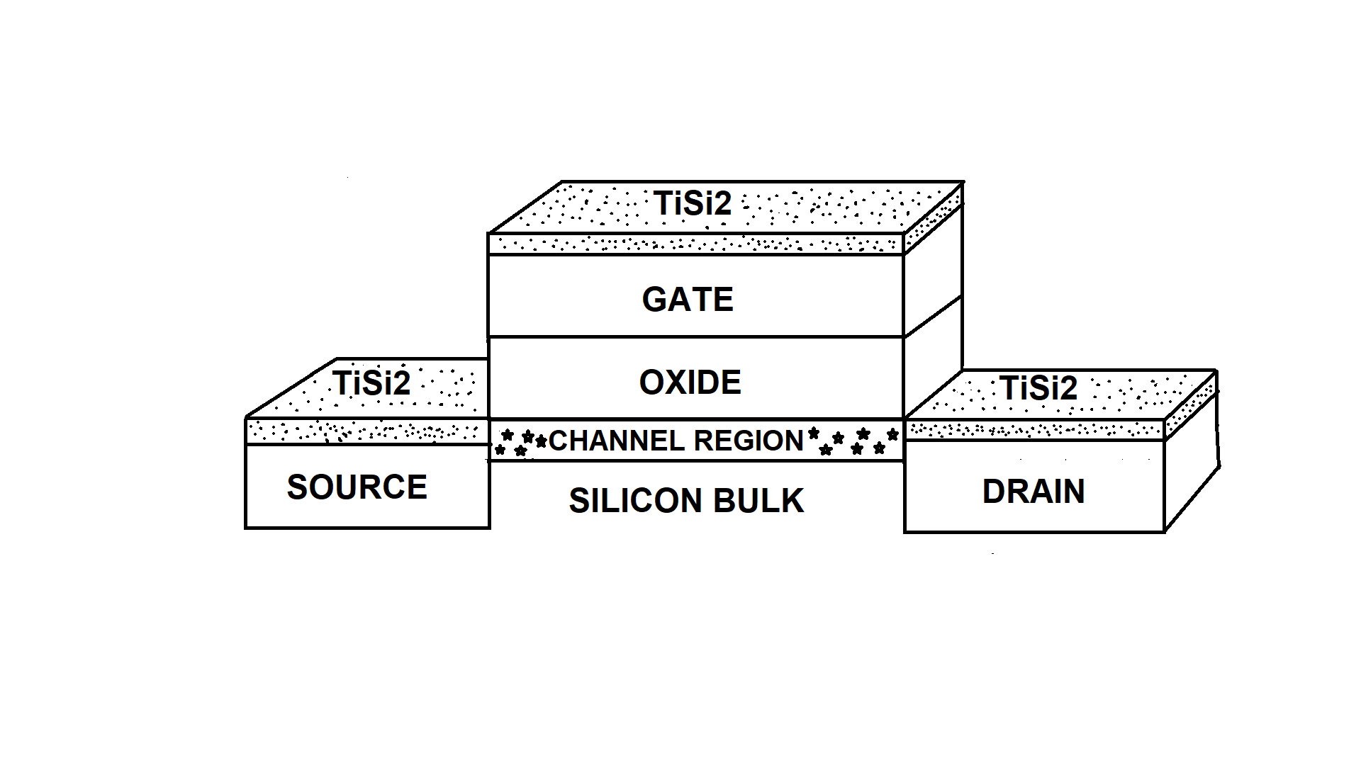 Figure 1: Cross section of a MOS transistor
Among all transition metal silicides, TiSi2 exhibits the lowest resistivity equal to 15 microohmcm.[5][6][7][8]
However, owing to the extreme reactivity of Ti and Si main diffusing species, the Ti-Si reaction also occurs in lateral directions, which induces shorting between gate and source-drain regions. The lateral growth is drastically reduced when the reaction is performed in nitrogen ambient[1][2]. Moreover, a TiN capping layer deposited on Ti/nSi Schottky diodes allows the barrier height (SBH) to be reduced by 80 meV which significantly save 15% (1.6 W) of self power consumption. Such an effect is due to nitrogen diffusion into the TiSix layer.[3]
Among all transition metal nitrides, TiN exhibits the highest melting point of 3220 K. Moreover, its low resistivity of 30 microohmcm, high thermodynamic stability, low friction constant, high wear and corrosion resistance make TiN good barrier for outward and inward diffusion of species, Schottky barrier contacts, transistor gate electrodes. [4][9] In contrast with Ti2N phase which crystallises either in the tetragonal or in the base-centred tetragonal structures with a small range of composition of about 33.3% and 37.5% of nitrogen, respectively, the TiNx phase has a NaCl-type cubic structure with a wide range of composition from x=0.6 to 1.2.[10][11].
TiN can be synthesized by DC or RF magnetron sputtering, pulsed laser irradiation. [4][9][11][12][13][14][15][16]
The Ti-Si reaction is very complex and diffusion limited. Two main mechanisms have been identified: The first one starts with the formation of a very thin and amorphous or thin grain silicide layer, which grows via Si and Ti diffusion through the Ti-Si interface. Si is the main diffusing species. The second one starts with an extensive Ti-Si intermixing via grain boundaries, which leads to a film of composition close to TiSi, which consists of very fine grains.[17] Various TixSiy compounds are identified and coexist, depending on the temperature of the process and annealing treatment duration.[3][6][8][17][18][19] Ti5Si3, Ti5Si4, TiSi and C49TiSi2 are the first phases to be synthesized. C49TiSi2 exhibits a high resistivity compared with C54TiSi2. It is the metastable form of TiSi2 and crystallizes in the base-centred orthorhombic structure at lower temperatures than C54TiSi2 of face-centred orthorhombic structure . Both compounds have the same atomic arrangement in the plane , they only differ from the stacking arrangement.[18] The TixSiy phases turn into the C54TiSi2 phase of low resistivity at higher temperatures.
A three-stage reaction model has been formulated to describe the process occuring in Ti films coated on Si wafers and annealed in a nitrogen ambient[1]. In this model, the Ti-SI interface is the centre of Si diffusion into the Ti lattice while the Ti surface is the centre of nitrogen diffusion into the Ti bulk. Both reactions are produced in opposite directions. The first stage is the initiation of the reaction, which consists of consuming the oxide remaining on Si wafers. In the second stage, both Ti-Si and Ti-N reactions are produced, which leads to the formation of Ti silicides and Ti nitrides. In the third stage, both phases interact and the result of the interaction depends on both thermodynamic and kinetic factors. According to thermodynamic data, since the enthalpy of formation of TiN is lower than the one of TiSi2, the formation of TiN must be promoted. The values are equal to -337.45 and -134.11 kJmol-1, respectively.[20]
The extensive Si diffusion at the interface between Ti films and Si wafers and the nitrogen diffusion into the film are illustrated in Figure 2. Secondary Ion mass spectrometry (SIMS) measurements have been realized by D. Mangin[21] on Ti thin films, 500 nm thick, heated at 800°C and processed in (Ar-33%N2-1%H2) expanding plasma for 1 h. They show that Si and nitrogen diffuse widely into the Ti film. Oxygen is also detected. It could be dissolved into the metal from the reaction between Ti and SiO2 and snow-ploughs ahead of growing Ti silicide films.[8]
Thin Ti films, 250 and 500 nm thick are deposited on Si wafers in an electron beam evaporator, under Ar gas at a pressure of 0.5 Pa by A. Bessaudou and A. Passelergue.[21] Si wafers are biased at -400 V and heated at 400°C.
Ti substrates of dimensions equal to 1 cm2 are placed on the heating substrate holder in the plasma reactor designed by J.L. Jauberteau and I. Jauberteau [21](Figure 2).
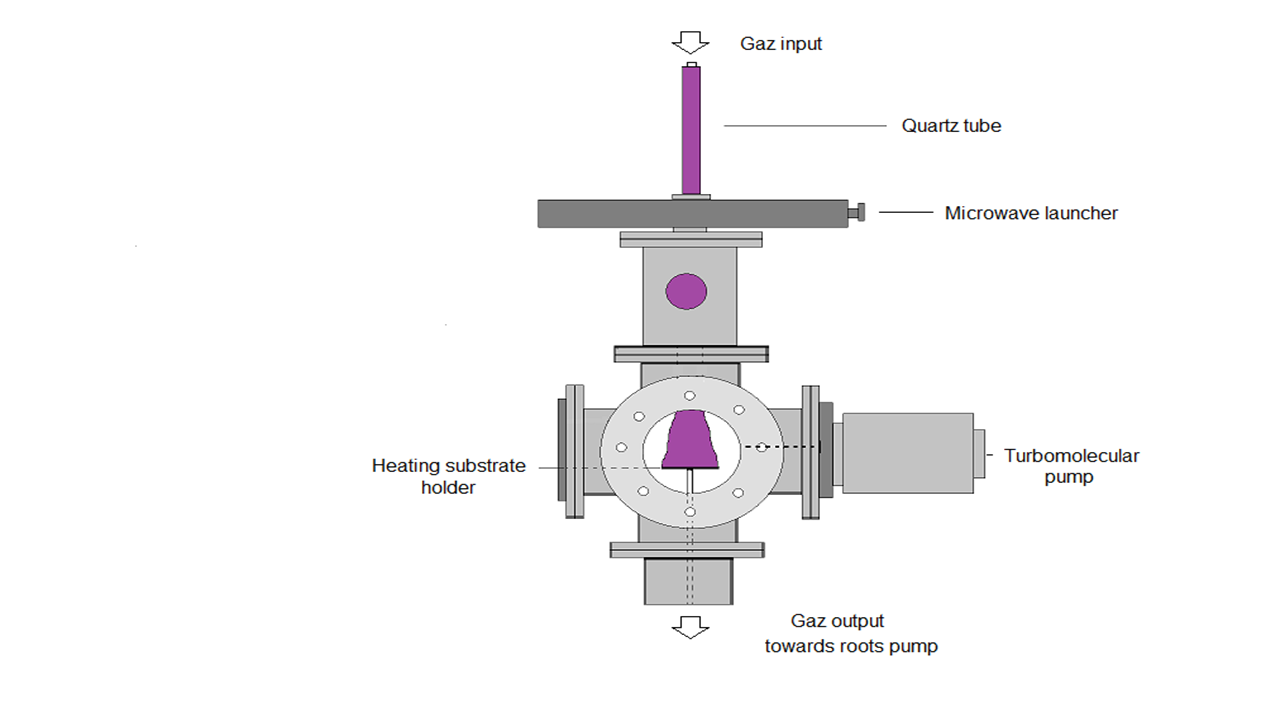
Figure 2: Experimental set-up /designed by J.L. Jauberteau and I. Jauberteau/.
The microwave discharge is produced in (Ar-33%N2-1%H2) gas mixture at a frequency of 2.45 GHz. The power of the discharge is mainly transferred to the electrons and then to other gaseous species by inelastic collisions. The plasma is expanded out of the centre of the discharge under the conditions of large density of electrons. These conditions depend on collision or collision less plasma and microwave frequency. The higher degree of ionization and dissociation makes the microwave plasma very interesting compared to other types of electrical excitations. The plasma forms a bright cone from the quartz tube exit up to the surface of the substrate (Figure 2). The electron density ranges between 0.03 and 0.15 x 10¹⁶ m-3and the electron energy ranges between 0.51 and 1.37 eV, under the experimental conditions used in this work. The ion energy at the sheath entrance is equal to about 0.1 eV. So, the physical sputtering induced in most of plasma processes as well as the heating effect can be neglected. Owing to the great reactivity of plasma species, chemical reactions at the surface of the metal are promoted. It has been shown that NHx and H reduce oxides and carbides formed during the process. The transfer of nitrogen into the metal film is then improved. Moreover, these species play a great role on the crystallographic structure of Mo2N [22].
C54TiSi2 crystallizes from TiSi and C49TiSi2 precursors in Ti Films , 250 and 500 nm thick heated at 600°C and processed in (Ar-33%N2-1%H2) expanding plasma, at a pressure of 0.13 kPa and a microwave power of 500 W.[21] The treatment is very efficient since no residual Ti or any other precursors have been identified in Ti films, 250 nm thick, processed for 30 min. X-ray diffraction (XRD) measurements have been performed by R. Mayet.[21] (Figure 3)
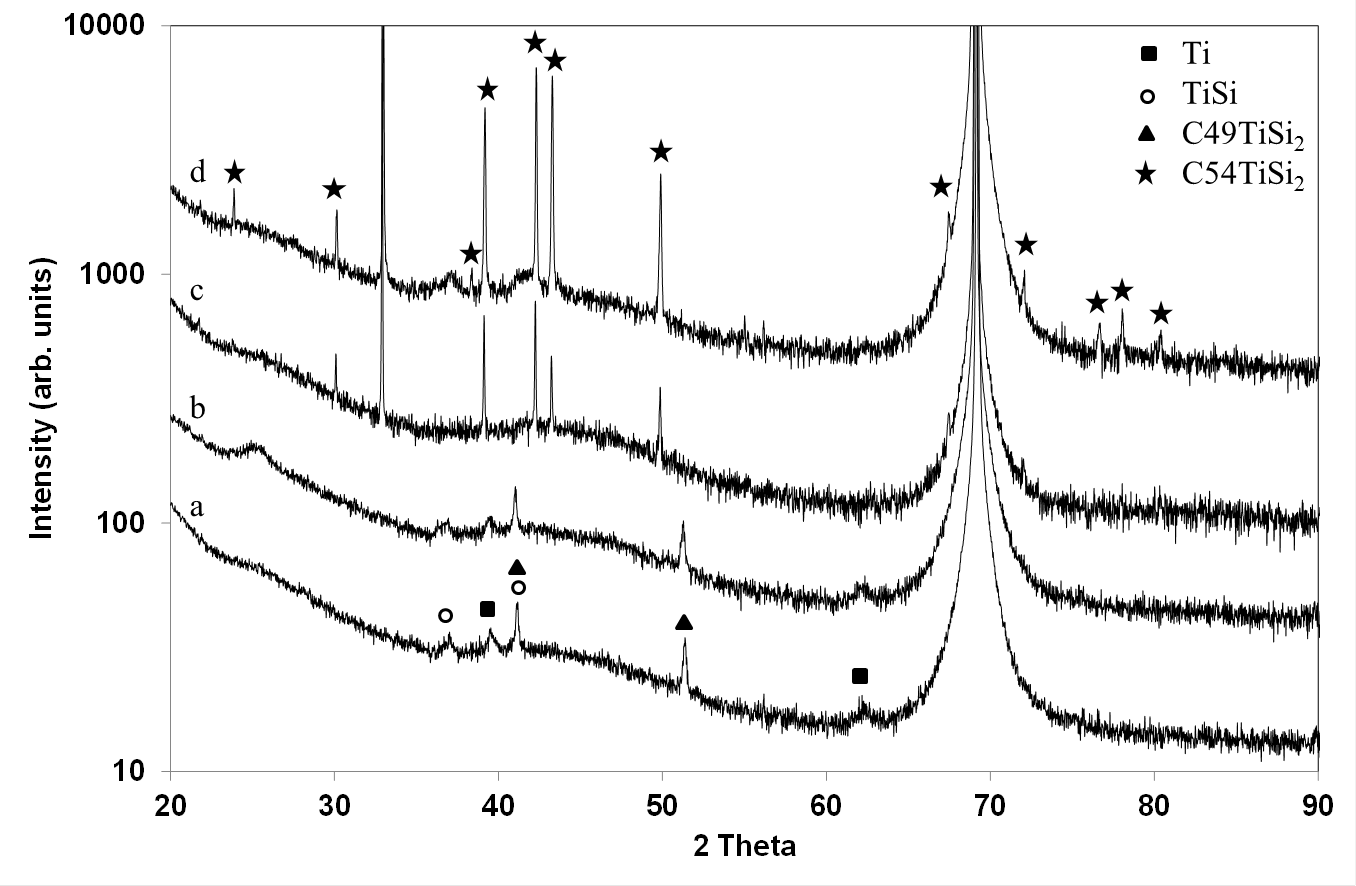
Figure 3: X-ray diffraction patterns of Ti films, 250 nm thick, heated at 500°C and processed in (Ar-33%N2-1%H2) plasma for 1.5 h (a) and 3 h (b) and Ti films, 250 nm thick and 500 nm thick, processed at 600°C in (Ar-33%N2-1%H2) for 30 min (c) and (d), respectively /XRD measurements performed by R. Mayet/.
TiSi and C49TiSi2 are the only phases to be observed at 500°C (Figure 3 (a) and (b)). The most intense (311), (040), (022) and (331) reflection lines of C54TiSi2, at Bragg angles equal to 39.2°, 42.3°, 43.3° and 49.9° (JCPDS card n° 00-035-0785) are identified in Figure 3 (c and d ). Since they are very thin and intense, C54TiSi2 is well crystallized and consists of large crystallites, which exhibit a (040) preferred orientation. Some TiSi precursors remain in Ti films, 500 nm thick (Figure 3 (d)).
In contrast with TiSi2 which exhibits a well crystallized structure, TiN is identified as an amorphous structure. Raman measurements have been carried out by J. Cornette.[21]
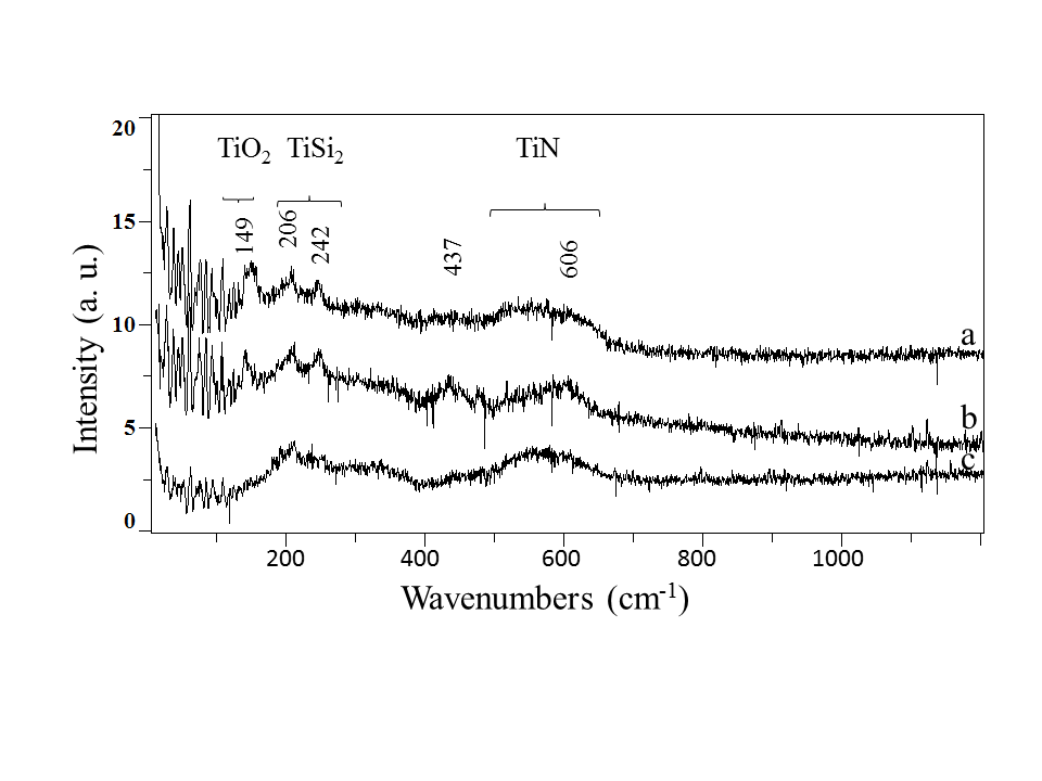
Figure 4: Raman scattering spectra of Ti films, 250 nm thick and 500 nm thick , heated at 600°C and processed in (Ar-33%N2-1%H2) plasma fo 30 min (a) and (b), respectively and Ti films, 500 nm thick, heated at 600°C and processed in (Ar-33%N2-1%H2) plasma for 3h (c) /Raman measurements performed by J. Cornette/.
Amorphous or disordered materials have broad Raman features with much weaker peak intensities compared with crystalline structure.[23]As seen in Figure 4, spectra (a) and (b) exhibit a relatively structured background, in the wave numbers range from 300 to 400 cm-1 and 450 to 600 cm-1, which are the frequency range of TiN vibrational bands . Owing to its Ti and N vacancies, TiN exhibits a first order Raman spectrum although it is a B1-structured material (Na-Cl type) of high symmetry. The lines correspond to TiSi2 and TiO2 in the form of anatase phase at 149 cm-1 and rutile phase at 437 and 606 cm-1. The intensity of vibrational bands of TiN increases with increasing treatment duration (Figure 4(c)), especially around 570 cm-1 which correspond to the most intense optic phonon (LO and TO modes) of TiN lattice vibrations [9][24]. In contrast, the most intense Raman features of TiO2 anatase phase disappears because of the reducing effect of NHx and H species, produced in the plasma.
TiN starts to crystallize at 800°C and grows at the expense of TiSi2 with increasing treatment duration. The growth of TiN crystallized phase is clearly seen on XRD patterns obtained by R. Mayet (Figure 5).[25]
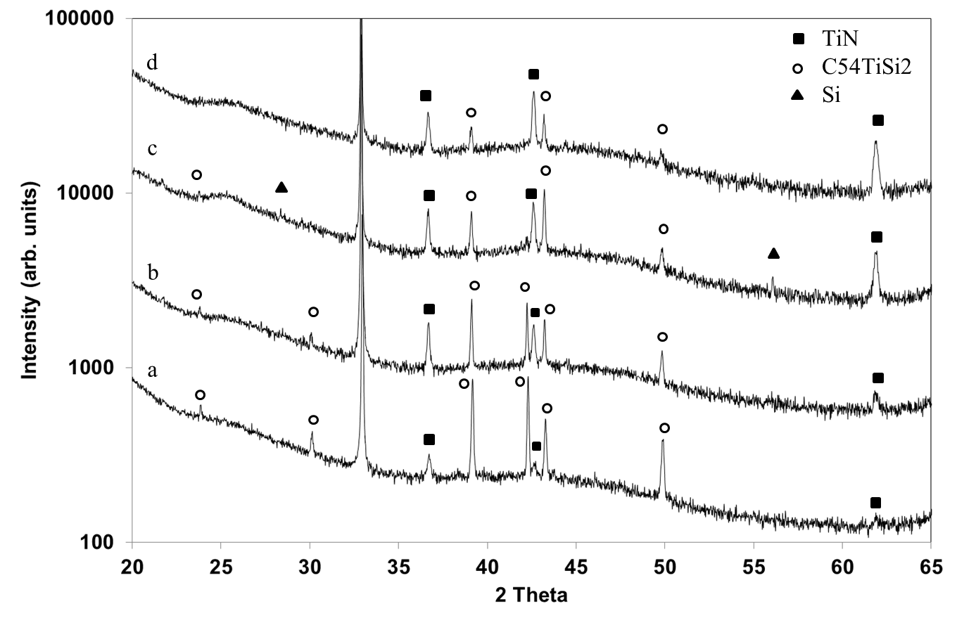
Figure 5: X-ray diffraction patterns of Ti films, 250 nm thick heated at 800°C and exposed to (Ar-33%N2-1%H2) plasma for 3 h (a), 6h (b), 12h (c) and 18 h (d) /XRD measurements performed by R. Mayet/.
TiN exhibits reflection lines at Bragg angles of 36.8°, 42.6° and 62° which correspond to the (111, (200) and (220) reflection lines, respectively (JCPDS card n° 04-004-2917). A simultaeous catastrophic decrease of the intensity of the C54TiSi2 (040) diffraction line and a strong increase of the TiN (220) diffraction line are shown, between 6 and 12 h of treatment duration (Figure 5 (b) and (c)). Such an effect might be assigned to an evolution of stresses in thin films with the growth of TiN phase. It is worth noting that the formation of silicides in metal films coated on Si substrates leads to compressive stresses. The elastic constants are higher in the [010] crystallographic direction[26]. TiN is formed from the reaction between TiSi2 and nitrogen. So, Si which is released during the reaction, is identified on Figure 5 (c) by the tiny diffraction lines at Bragg angles equal to 28.5° and 56.1° corresponding to intense (111) and (311)reflection lines of polycrystalline Si (JCPDS card n°04-001-7247). Then, Si moves into the lower silicide region and segregates at the Ti/Si interface where it grows epitaxially.[25] The epitaxial growth of Si is proved by the lack of diffraction lines in Figure 5 (d).
The growth of TiN crystallized film at the expense of TiSi2 film is confirmed on cross-sectional transmission electron micrographs and selected area electron diffraction (SAED) patterns, which allows the phase identification to be performed. (Figure 6). The transmission electron microscopy (TEM) and electron diffraction investigations have been conducted by P. Carles[25].
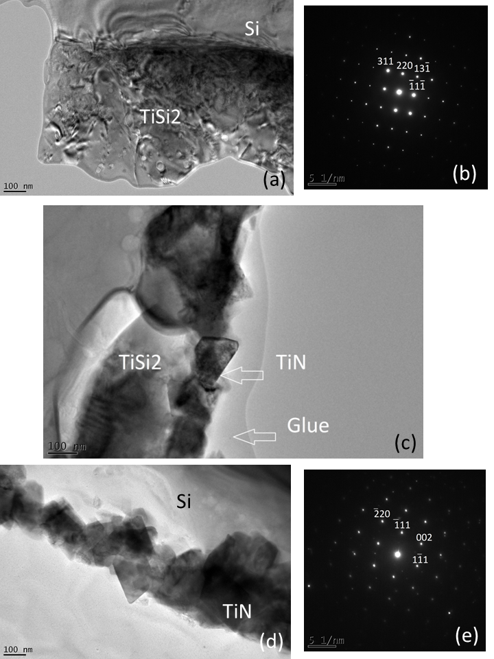
Figure 6: Cross sectional transmission electron micrographs (CSTEM) of the Ti film, 500 nm thick,processed at 800°C in (Ar-33%N2-1%H2) plasma for 1 h (a) and indexed SAED pattern of a region of the film with the zone axis [-112] (b). CSTEM of Ti films, 250 nm thick, processed at 800°C in (Ar-33%N2-1%H2) plasma for 6h, displaying both TiN and TiSi2 layers (c). CSTEM of Ti films, 250 nm thick, processed at 800°C in (Ar-33%N2-1%H2) plasma for 18h (d) and indexed SAED of TiN crystals viewed with the zone axis [110] (e) /TEM and SAED measurements performed by P. Carles/.
Ti films, 500 nm thick, heated at 800°C and exposed to (Ar-33%N2-1%H2) plasma for 1 h mainly consist of C54TiSi2 crystallites of large size ranging between 200 and 500 nm (Figure 6a). The thickness of the film has increased, compared with the untreated film, because of the intensive diffusion and intermixing of Si and Ti. It varies between 850 and 1000 nm. The corresponding SAED confirms the crystalline structure of C54TiSi2 (Figure 6b). On this pattern , the incident electron beam is parallel to the [-112] crystallographic direction (zone axis). So, the (-112) plane is observed under these conditions. The length of diffraction vectors and the angles between the diffraction vectors are compared with d spacings reported in the corresponding JCPDS card and the calculated angle values, respectively.
Longer plasma exposures lead to the growth of TiN crystallites. Ti films, 250 nm thick, heated at 800°C and exposed to the plasma for 6 h is formed of two distinct layers. The first one, next to the film surface consists of square shaped crystals of TiN, 50-100 nm large whereas the second one, next to the substrate, consists of round shaped crystals of TiSi2, about 300 nm large. As previously seen for films, 500 nm thick, the film thickness has increased up to 400-500 nm. A 18 h plasma exposure leads to the formation of a film only consisting of TiN crystals, about 200 nm wide (Figure 6d). The thickness of the film did not change from 6 h to 18 h of treatment duration since it is determined from the initial growth of the TiSi2 phase. TiN crystals are oriented along the [110] crystallographic direction (zone axis) ( Figure 6e). So, they tend to display a flattened morphology with the [110] direction perpendicular to the flat surface. Growth steps have been identified in [220] crystallographic direction formed with zigzag {111} facets as in Pt crystals.[25] The TiSi2 films completely turned into TiN, under these conditions. TiN is produced from the reaction between TiSi2 and nitrogen and Si is released during the reaction. The large islands of white colour, next to the Si substrate consists of amorphous Si which segregated at the surface of the substrate.
The reaction process leading to the formation and growth of silicides and nitrides in thin Ti films heated at various temperatures and exposed to (Ar-N2-H2) plasma is thermodynamically and kinetically controlled. It involves the following key stages:
1. Si diffuses into grain boundaries and grains of Ti. Simultaneously, NHx species produced in (Ar-N2-H2) plasma react on the Ti surface and N diffuses into the metal film via grain boundaries (Temperature equal to about 400°C)
2. Formation and crystallization of precursors of C54TiSi2 compound such as TiSi and C49TiSi2 which turn into C54TiSi2 at 600°C. Formation and growth of TiN of amorphous structure in opposite direction. The Ti-Si reaction is very fast since Ti films, 250 nm thick processed for 30 min only consists of cristallized C54TiSi2. Amorphous TiN grows with increasing treatment duration. It is expected that, according to the model of reaction described in section 3.2., TiSi2 and TiN interact and the result of interaction depend on thermodynamic and kinetic factors. According to thermodynamic factors TiN is expected to grow at the expense of TiSi2. It has previously been reported that, the nitridation of TiSi2 does not occur at measurable rate at temperatures below 800°C.[27]
3. Crystallisation of TiN at 800°C and growth at the expense of TiSi2 in agreement with the respective enthalpies of formation of both compounds.
4. All TiSi2 films turned into TiN films and Si according to the reaction between TiSi2 and nitrogen. Si which has been released during the reaction, moved to the Si substrate, segregated on it and grew in the epitaxial direction.