Submitted Successfully!
To reward your contribution, here is a gift for you: A free trial for our video production service.
Thank you for your contribution! You can also upload a video entry or images related to this topic.
Version Summary Created by Modification Content Size Created at Operation
1 + 1770 word(s) 1770 2021-10-18 11:42:06 |
2 format corrected. + 137 word(s) 1907 2021-11-01 10:07:17 | |
3 ref. added. + 138 word(s) 1908 2021-11-01 10:15:35 | |
4 ref. added. + 138 word(s) 1908 2021-11-01 10:19:39 | |
5 corrected the format Meta information modification 1908 2021-11-01 10:23:26 | |
6 figure added. + 15 word(s) 1923 2021-11-01 10:32:08 | |
7 format corrected. Meta information modification 1923 2021-11-02 08:00:09 |

Video Upload Options

Do you have a full video?

Confirm

Are you sure to Delete?
Cite
If you have any further questions, please contact Encyclopedia Editorial Office.
Chiu, Y. Profiling the Cycling-Induced Oxide Trapped Charge. Encyclopedia. Available online: https://encyclopedia.pub/entry/15547 (accessed on 18 April 2024).
Chiu Y. Profiling the Cycling-Induced Oxide Trapped Charge. Encyclopedia. Available at: https://encyclopedia.pub/entry/15547. Accessed April 18, 2024.
Chiu, Yung-Yueh. "Profiling the Cycling-Induced Oxide Trapped Charge" Encyclopedia, https://encyclopedia.pub/entry/15547 (accessed April 18, 2024).
Chiu, Y. (2021, October 29). Profiling the Cycling-Induced Oxide Trapped Charge. In Encyclopedia. https://encyclopedia.pub/entry/15547
Chiu, Yung-Yueh. "Profiling the Cycling-Induced Oxide Trapped Charge." Encyclopedia. Web. 29 October, 2021.
Profiling the Cycling-Induced Oxide Trapped Charge
Edit

NAND Flash memories have gained tremendous attention owing to the increasing demand for storage capacity. This implies that NAND cells need to scale continuously to maintain the pace of technological evolution. Even though NAND Flash memory technology has evolved from a traditional 2D concept toward a 3D structure, the traditional reliability problems related to the tunnel oxide continue to persist.

NAND Flash memory endurance reliability oxide trapped charge

1. Introduction

The emergence of NAND Flash memories has revolutionized the data storage industry over the last few decades. NAND Flash devices are used in a wide range of applications in everyday consumer electronics such as laptops, tablets, and smart wearable devices. The first NAND-structured cell was invented in 1987 by Masuoka et al. [1] at Toshiba Corp. Since then, several improvements have been proposed to lower the power consumption of these cells and to enable the contents of the entire chip to be erased at once [2][3][4][5][6][7]. More recently, its application range has been expanded such that it has become the main storage element, in that solid-state drives (SSDs) are gradually replacing hard disk drives (HDDs) [8][9]. Furthermore, it is increasingly adopted for enterprise-class storage systems. As a result, the size of NAND cells has aggressively shrunk to continuously promote this evolution. However, the ever-shrinking dimensions of the NAND cell create additional challenges in terms of the endurance and retention characteristics, such as random telegraph noise (RTN) fluctuations of the threshold voltage ( V T ) [10][11][12], charge trapping/detrapping mechanisms [13][14][15], electron injection statistics [16][17], and V T distribution widening due to parasitic coupling effects [18][19].

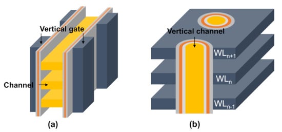
Three-dimensional (3D) NAND Flash memories can be considered as a breakthrough to continue to deliver increasing bit density and reduce the bit cost [20]. 3D NAND Flash technology can utilize either floating gate (FG)- or charge trapping (CT)-type cells. Most of the 3D NAND reported to date are CT-type, owing to the simpler fabrication process [21]. The 3D NAND array architecture can be categorized into the following two classes depending on the direction of channel, as schematically shown in Figure 1 : vertical gate 3D NAND architecture, which was proposed by Samsung Electronics in 2009 [22]; and vertical channel 3D NAND architecture. There are two main cell structure types that use vertical channels, namely bit cost scalable (BiCS), which was proposed by Toshiba Corp. in 2007 [23][24], and terabit cell array transistor (TCAT), which was developed by Samsung Electronics in 2009 [25]. TCAT subsequently evolved into V-NAND architecture, which has 32-stacked word line (WL) layers [26][27][28]. The industry has moved beyond 12x-stacked WL layers and achieved a 17x-stacked V-NAND [29][30]. As the memory industry transitions from planar to 3D scaling, traditional device reliability issues must still be considered. The Fowler Nordheim (FN) tunneling mechanism is commonly used in both planar and 3D NAND cells during programming and erasing (P/E) operations [31]. This mechanism leads to the formation of trap states in the tunneling oxide, and thus degrades the oxide reliability. Therefore, overcoming the reliability problems related to the oxide trap is critically important for the development of future advanced NAND Flash memories.

Electronics 10 02492 g001 550
Figure 1. Schematic diagrams of 3D NAND architecture: (a) vertical gate and (b) vertical channe

2. Shift in the Midgap Voltage

Generally, the midgap voltage ( Δ V M G ) during P/E operations is described by a set of two components [32]: the first is the electrostatic shift (ES) that is caused by the creation of oxide trapped charges ( Q T ), and the other is the tunneling shift (TS) that is related to the change in the number of floating-gate charges ( Q F G ). Notably, these two components mutually influence each other. The former deforms the tunneling barrier for P/E operations and thus reduces the number of storage electrons. Δ V M G can be expressed as the sum of these two components.

Δ V M G = Q T C i + Δ Q F G C I P D (1)

where Ci and CIPD are the tunneling oxide and the interpoly dielectric capacitance, respectively.

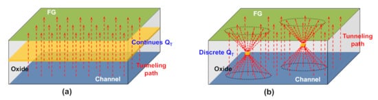
Several approaches have been proposed to separate the ES and TS values from Δ V M G . The first category of methods is based on indirect measurements. For example, the Δ V M G in the programming and erasing states combined with tunneling-based modeling is commonly monitored to extract the Q T distribution from Q F G in NAND Flash memories. Q F G has been presented by a sheet charge located at fixed distance from the channel in the majority of the literature [32][33][34]. Under this assumption, the tunneling current is calculated straightforwardly along the direction perpendicular to the channel by using the Wentzel–Kramers–Brillouin (WKB) approximation, as schematically shown in Figure 2 a. However, as the cell sizes are aggressively shrunk to the nanoscale regime, they are adversely affected by the discrete nature of Q T . Thus, we must consider all possible tunneling paths across the defective oxide [35][36], as schematically shown in Figure 2 b, which increases the computational time and complexity of the method.

Electronics 10 02492 g002 550
Figure 2. Schematic diagrams of all the possible tunneling paths by the (a) continuous and (b) discrete QT during P/E cycles.

The second category of methods is based on the direct extraction of Q T and Q F G using a special test device [37][38]. The cross-sectional view and equivalent circuit of the test structure are shown in Figure 3 . The device is composed of two memory cells: one with a thick tunneling oxide, referred to as a high-voltage (HV) cell, and the other with a thin tunneling oxide, referred to as a low-voltage (LV) cell. Notably, these two cells have a common FG/common control gate (CG) configuration. During P/E operations, FN tunneling occurs only through the oxide of the LV cell, thus degrading the oxide of this cell. The ES resulting from Q T is expressed as [38]

  ES = γ Δ V T L V Δ V T H V = 1 ε o x 0 T O X ρ · x d x (2)

where γ is the coupling ratio between the FG and CG, ρ is the density of Q T , and Δ V T L V and Δ V T H V are the V T shifts of the LV and HV cells after P/E cycles, respectively. Unfortunately, the size of the test device ( L = 4 µm) is relatively large compared to that of conventional NAND Flash memories, yet it is necessary to continuously evaluate these miniaturized and new device structures. Moreover, this approach can only provide average information for a relatively large sample region rather than statistical information.

3. ∆Gm, max Statistics

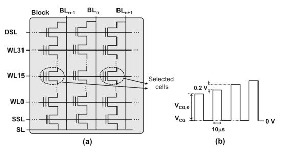
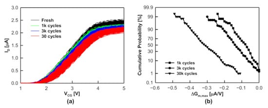
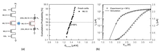
Experiments are carried out in 2D FG-type NAND Flash memory chip. In the NAND array, a string is composed of 32-unit cells, a source-select transistor, and a drain-select transistor, as schematically shown in Figure 4 a. The control gates, source-select transistors, and drain-select transistors are connected across different strings to constitute the wordline (WL), source select line (SSL), and drain select (DSL), respectively. The strings are connected to a common sourceline (SL) and bitlines (BLs). The channel length ( L ) and width ( W ) are both 42 mm, and the tunneling oxide thickness ( T o x ) is 8 nm. The measurement scheme was as follows: the program operation is performed by adopting the incremental step pulse programming (ISPP) technique [39] with a starting CG voltage ( V C G , 0 ,0) in increments of 0.2 V with a duration of 10 µs, as schematically shown in Figure 4 b, driving the selected cells to the desired V T level. The erase operation is performed on blocks by adopting the incremental step pulse erasing (ISPE; similar to the ISPP) technique. Because it is not possible to apply high negative voltages in NAND chips, a high positive voltage is applied to the p-well. As a result, all cells in the block were erased simultaneously. During the read operation, the CG gate voltage was swept from 0 V to 5 V to harvest the maximum transconductance reduction ( Δ G m , m a x ). Figure 5 a shows the I D V C G characteristics of the 200 randomly selected cells on WL15 in NAND strings before cycling and after 1 k, 3 k, and 30 k P/E cycles, respectively. Then, the corresponding Δ G m , m a x distribution can be obtained, as shown in Figure 5 b. Notably, the endurance test and Δ G m ,m a x monitoring were performed at room temperature. The mean value of Δ G m , m a x ( Δ G ¯ m , m a x ) is clearly observed to increase, and the distribution to become wider, as the number of cycles increases. This suggests that the Δ G m , m a x distribution will be a good parameter for evaluating the oxide degradation.

Electronics 10 02492 g004 550
Figure 4. Schematic view of (a) NAND Flash array and (b) ISPP operation. Adapted from [40].
Electronics 10 02492 g005 550
Figure 5. (a) I D V C G Characteristics and (b) cumulative ΔGm,max statistics of the read cells on WL15 as a function of the number of P/E cycles. Adapted from [39].

Monte Carlo simulations have been used in an attempt to extract information about Q T from the measured Δ G m ,m a x distribution. A NAND string can be modeled to have a selected cell with equivalent source and drain resistances ( R S and R D ), as shown in Figure 6 a. The equivalent ( R S and R D can be extracted from the monitoring of the transconductance of the read cells for different positions along the NAND string [41]. The equivalent R S and R D are 130 kΩ and 138.2 kΩ, respectively. The TCAD simulations used a 3D drift-diffusion equation and coupled with the Shockley–Read– Hall model for generation/recombination and mobility models (including the electric field dependence, doping-dependent modification, and surface mobility degradation). To determine the Δ G ¯ m , m a x statistics accurately, the simulated I D V C G characteristic of the fresh cell is calibrated with experimental data at a probability level p = 50% , as shown in Figure 6 b. The simulation was in good agreement with the experimental results. After calibrating the equivalent resistances, the Monte-Carlo-based method was adopted to evaluate the concentration of Q T ( Q T C ) after P/E cycles, as schematically shown in Figure 7 . The step-by-step procedure is as follows: First, discrete Q T is randomly generated following a uniform distribution in a cuboid volume 420  nm   × 840  nm   × 8  nm in size (i.e., 20  L   × 10  W   × T o x ), with an equivalent Q T C . Notably, the discrete Q T is treated as a negative point charge corresponding to one electron because the electron mobility is degraded by the Coulomb repulsion.

Electronics 10 02492 g006 550
Figure 6. (a) Schematic circuit diagram of a NAND string and an equivalent model when cells on WL15 are read. (b) Comparison between measured and simulated I D V C G curve of cells on WL15 at p=50%, plotted on the linear and logarithmic scales. Adapted from [39].
Electronics 10 02492 g007 550
Figure 7. Schematic diagram of the random discrete Q T generating algorithm. Adapted from [39].

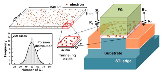
Second, the cuboid is partitioned into 200 sub-cuboids and then mapped into the tunneling oxide region. Thus, the numbers of discrete Q T in these 200 cases approximately follow a Poisson distribution, as shown in Figure 7 . Finally, a comparison of the simulated and measured Δ G m ,m a x statistics allowed us to evaluate the Q T C during P/E cycles.

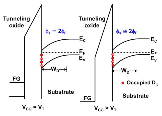
Moreover, even though the simulation does not directly account for interface trap ( D i t ) generation, the effect thereof is reflected in the model. The measured I D V C G characteristics indicated that the transconductance reached a maximum when V C G slightly exceeded D i t ; therefore, the occupied D i t can be considered as a fixed Q T located at the silicon/oxide interface because the bending of the surface potential remains almost unchanged [42] (see Figure 8 ).

Figure 8. Band diagram and trap occupation of interface trap states at different biases. Reprinted from [39].

References

  1. Masuoka, F.; Momodomi, M.; Iwata, Y.; Shirota, R. New ultra high density EPROM and Flash EEPROM with NAND structure cell. In Proceedings of the 1987 International Electron Devices Meeting, New York, NY, USA, 6–9 December 1987; pp. 552–555.
  2. Shirota, R.; Itoh, Y.; Nakayama, R.; Momodomi, M.; Inoue, S.; Kirisawa, R.; Iwata, Y.; Chiba, M.; Masuoka, F. A new NAND cell for ultra high density 5 V-only EEPROMs. In Proceedings of the 1988 Symposium on VLSI Technology—Digest of Technical Papers, San Diego, CA, USA, 10–13 May 1988; pp. 33–34.
  3. Momodomi, M.; Kirisawa, R.; Nakayama, R.; Aritome, S.; Endoh, T.; Itoh, Y.; Iwata, Y.; Oodaira, H.; Tanaka, T.; Chiba, M.; et al. New device technologies for 5 Vonly 4 Mb EEPROM with NAND structure cell. In Proceedings of the 1988 International Electron Devices Meeting, San Francisco, CA, USA, 11–14 December 1988; pp. 412–415.
  4. Momodomi, M.; Itoh, Y.; Shirota, R.; Iwata, Y.; Nakayama, R.; Kirisawa, R.; Tanaka, T.; Aritome, S.; Endoh, T.; Ohuchi, K.; et al. An experimental 4-Mbit CMOS EEPROM with a NAND structure cell. IEEE J. Solid-State Circuits 1989, 24, 1238–1243.
  5. Iwata, Y.; Momodomi, M.; Tanaka, T.; Oodaira, H.; Itoh, Y.; Nakayama, R.; Kirisawa, R.; Aritome, S.; Endoh, T.; Shirota, R.; et al. A high-density NAND EEPROM with block-page programming for microcomputer applications. IEEE J. Solid-State Circuits 1990, 25, 417–424.
  6. Kirisawa, R.; Aritome, S.; Nakayama, R.; Endoh, T.; Shirota, R.; Masuoka, F. A NAND structured cell with a new programming technology for highly reliable SV-only Flash EEPROM. In Proceedings of the 1988 Symposium on VLSI Technology—Digest of Technical Papers, Honololu, HI, USA, 4–7 June 1990; pp. 129–130.
  7. Aritome, S.; Shirota, R.; Kirisawa, R.; Endoh, T.; Nakayama, N.; Sakui, K.; Masuoka, F. A reliable bi-polarity write/erase technology in flash EEPROMs. In Proceedings of the 1988 International Electron Devices Meeting, San Francisco, CA, USA, 9–12 December 1990; pp. 111–114.
  8. Micheloni, R.; Marelli, A.; Eshghi, K. Inside Solid State Drives (SSDs); Springer: New York, NY, USA, 2013.
  9. Spinelli, A.; Compagnoni, C.; Lacaita, A. Reliability of NAND Flash Memories: Planar Cells and Emerging Issues in 3D Devices. Computers 2017, 6, 16.
  10. Ghetti, A.; Monzio Compagnoni, C.; Spinelli, A.S.; Visconti, A. Comprehensive analysis of random telegraph noise instability and its scaling in deca-nanometer Flash memories. IEEE Trans. Electron Devices 2009, 56, 1746–1752.
  11. Kurata, H.; Otsuga, K.; Kotabe, A.; Kajiyama, S.; Osabe, T.; Sasago, Y.; Narumi, S.; Tokami, K.; Kamohara, S.; Tsuchiya, O. The impact of random telegraph signals on the scaling of multilevel Flash memories. In Proceedings of the 2006 Symposium on VLSI Technology (VLSI-Technology), Honolulu, HI, USA, 13–15 June 2006; pp. 112–113.
  12. Tega, N.; Miki, H.; Osabe, T.; Kotabe, A.; Otsuga, K.; Kurata, H.; Kamohara, S.; Tokami, K.; Ikeda, Y.; Yamada, R. Anomalously large threshold voltage fluctuation by complex random telegraph signal in floating gate Flash memory. In Proceedings of the 2006 International Electron Devices Meeting (IEDM), San Francisco, CA, USA, 11–13 December 2006; pp. 491–494.
  13. Resnati, D.; Nicosia, G.; Paolucci, G.M.; Visconti, A.; Monzio Compagnoni, C. Cycling-induced charge trapping/detrapping in Flash memories—Part I: Experimental evidence. IEEE Trans. Electron Devices 2016, 63, 4753–4760.
  14. Mielke, N.; Belgal, H.; Kalastirsky, I.; Kalavade, P.; Kurtz, A.; Meng, Q.; Righos, N.; Wu, J. Flash EEPROM threshold instabilities due to charge trapping during program/erase cycling. IEEE Trans. Device Mater. Reliab. 2004, 4, 335–344.
  15. Paolucci, G.M.; Monzio Compagnoni, C.; Miccoli, C.; Spinelli, A.S.; Lacaita, A.L.; Visconti, A. Revisiting charge trapping/detrapping in Flash memories from a discrete and statistical standpoint—Part I: VT instabilities. IEEE Trans. Electron Devices 2014, 61, 2802–2810.
  16. Monzio Compagnoni, C.; Spinelli, A.S.; Gusmeroli, R.; Beltrami, S.; Ghetti, A.; Visconti, A. Ultimate accuracy for the NAND Flash program algorithm due to the electron injection statistics. IEEE Trans. Electron Devices 2008, 55, 2695–2702.
  17. Monzio Compagnoni, C.; Gusmeroli, R.; Spinelli, A.S.; Visconti, A. Analytical model for the electron-injection statistics during programming of nanoscale NAND Flash memories. IEEE Trans. Electron Devices 2008, 55, 3192–3199.
  18. Nishi, Y. (Ed.) Advances in Non-Volatile Memory and Storage Technology; Woodhead Publishing: Cambridge, UK, 2014.
  19. Lee, J.-D.; Hur, S.-H.; Choi, J.-D. Effects of floating-gate interference on NAND flash memory cell operation. IEEE Electron Device Lett. 2002, 23, 264–266.
  20. Goda, A.; Parat, K. Scaling directions for 2D and 3DNAND cells. In Proceedings of the 2012 IEEE International Electron Devices Meeting (IEDM), San Francisco, CA, USA, 10–13 December 2012.
  21. Goda, A. 3-D NAND technology achievements and future scaling perspectives. IEEE Trans. Electron Devices 2020, 67, 1373–1381.
  22. Kim, W.; Choi, S.; Sung, J.; Lee, T.; Park, C.; Ko, H.; Jung, J.; Yoo, I.; Park, Y. Multi-layered vertical gate NAND Flash overcoming stacking limit for terabit density storage. In Proceedings of the 2009 Symposium on VLSI Technology, Kyoto, Japan, 15–17 June 2009; pp. 188–189.
  23. Tanaka, H.; Kido, M.; Yahashi., K.; Oomura, M.; Katsumata, R.; Kito, M.; Fukuzumi, Y.; Sato, M.; Nagata, Y.; Matsuoka, Y.; et al. Bit cost scalable technology with punch and plug process for ultra high density flash memory. In Proceedings of the 2007 Symposium on VLSI Technology, Kyoto, Japan, 12–14 June 2007; pp. 14–15.
  24. Fukuzumi, Y.; Katsumata, R.; Kito, M.; Kido, M.; Sato, M.; Tanaka, H.; Nagata, Y.; Matsuoka, Y.; Iwata, Y.; Aochi, H.; et al. Optimal integration and characteristics of vertical array devices for ultra-high density, bit-cost scalable flash memory. In Proceedings of the 2007 International Electron Devices Meeting (IEDM), Washington, DC, USA, 10–12 December 2007; pp. 449–452.
  25. Jang, J.; Kim, H.-S.; Cho, W.; Cho, H.; Kim, J.; Shim, S.I.; Jang, Y.; Jeong, J.-H.; Son, B.-K.; Kim, D.-W.; et al. Vertical cell array using TCAT (terabit cell array transistor) technology for ultra high density NAND flash memory. In Proceedings of the 2009 Symposium on VLSI Technology, Kyoto, Japan, 15–17 June 2009; pp. 192–193.
  26. Elliott, J.; Jung, E.S. Ushering in the 3D Memory Era with V-NAND. In Proceedings of the Flash Memory Summit, Santa Clara, CA, USA, 13–15 August 2013.
  27. Park, K.T.; Byeon, D.S.; Kim, D.H. A world’s first product of three-dimensional vertical NAND Flash memory and beyond. In Proceedings of the 2014 14th Annual Non-Volatile Memory Technology Symposium (NVMTS), Jeju Island, Korea, 27–29 October 2014; pp. 1–5.
  28. Park, K.T.; Nam, S.; Kim, D.; Kwak, P.; Lee, D.; Choi, Y.H.; Choi, M.H.; Kwak, D.H.; Kim, D.H.; Kim, M.S.; et al. Three-Dimensional 128 Gb MLC Vertical nand Flash Memory With 24-WL Stacked Layers and 50 MB/s High-Speed Programming. IEEE J. Solid State Circuit 2015, 50, 204–213.
  29. Kang, D.; Kim, M.; Jeon, S.-C.; Jung, W.; Park, J.; Choo, G.; Shim, D.-K.; Kavala, A.; Kim, S.-B.; Kang, K.-M.; et al. A 512Gb 3-bit/cell 3D 6th-generation V-NAND flash memory with 82MB/s write throughput and 1.2Gb/s interface. In Proceedings of the 2019 IEEE International Solid-State Circuits Conference (ISSCC), San Francisco, CA, USA, 17–21 February 2019; pp. 216–218.
  30. Cho, J.; Chris Kang, D.; Park, J.; Nam, S.-W.; Song, J.-H.; Jung, B.-K.; Lyu, J.; Lee, H.; Kim, W.-T.; Jeon, H.; et al. A 512Gb 3b/Cell 7th-generation 3D-NAND flash memory with 184MB/s write throughput and 2.0Gb/s interface. In Proceedings of the 2021 IEEE International Solid-State Circuits Conference (ISSCC), San Francisco, CA, USA, 13–22 February 2021; pp. 426–428.
  31. Monzio Compagnoni, C.; Goda, A.; Spinelli, A.S.; Feeley, P.; Lacaita, A.L.; Visconti, A. Reviewing the evolution of the NAND Flash technology. Proc. IEEE 2017, 105, 1609–1633.
  32. Fayrushin, A.; Lee, C.-H.; Park, Y.; Choi, J.-H.; Chung, C. Unified endurance degradation model of floating gate NAND flash memory. IEEE Trans. Electron Devices 2013, 60, 2031–2037.
  33. Xia, Z.; Kim, D.S.; Jeong, N.; Kim, Y.-G.; Kim, J.-H.; Lee, K.-H.; Park, Y.-K.; Chung, C.; Lee, H.; Han, J. Comprehensive modeling of NAND flash memory reliability: Endurance and data retention. In Proceedings of the IEEE International Reliability Physics Symposium (IRPS), Anaheim, CA, USA, 15–19 April 2012; pp. MY.5.1–MY.5.4.
  34. Yang, B.-J.; Wu, Y.-T.; Chiu, Y.-Y.; Kuo, T.-M.; Chang, J.-H.; Wang, P.-Y.; Shirota, R. Evaluation of the role of deep trap state using analytical model in the program/erase cycling of NAND flash memory and its process dependence. IEEE Trans. Electron Devices 2018, 65, 499–506.
  35. Watanabe, H.; Yao, K.; Lin, J. Numerical study of very small floating islands. IEEE Trans. Electron. Devices 2014, 61, 1145–1152.
  36. Lin, P.-J.-J.; Lee, C.-A.-A.; Yao, C.-W.-K.; Lin, H.-J.-V.; Watanabe, H. Localized tunneling phenomena of nanometer scaled high-K gate-stack. IEEE Trans. Electron Devices 2017, 64, 3077–3083.
  37. Shirota, R.; Yang, B.-J.; Chiu, Y.-Y.; Chen, H.-T.; Ng, S.-F.; Wang, P.-Y.; Chang, J.-H.; Kurachi, I. New accurate method to analyze both floating gate charge and tunnel oxide trapped charge profile in NAND flash memory. In Proceedings of the IEEE International Memory Workshop (IMW), Taipei, Taiwan, 18–21 May 2014; pp. 55–58.
  38. Shirota, R.; Yang, B.-J.; Chiu, Y.-Y.; Chen, H.-T.; Ng, S.-F.; Wang, P.-Y.; Chang, J.-H.; Kurachi, I. New method to analyze the shift of floating gate charge and generated tunnel oxide trapped charge profile in NAND flash memory by program/erase endurance. IEEE Trans. Electron Devices 2015, 62, 114–120.
  39. Hemink, G.J.; Tanaka, T.; Endoh, T.; Aritome, S.; Shirota, R. Fast and accurate programming method for multi-level NAND EEPROMs. In Proceedings of the 1995 Symposium on VLSI Technology—Digest of Technical Papers, Kyoto, Japan, 6–8 June 1995; pp. 129–130.
  40. Chiu, Y.-Y.; Lin, I.-C.; Chang, K.-C.; Yang, B.-J.; Takeshita, T.; Yano, M.; Shirota, R. Transconductance distribution in program/erase cycling of NAND flash memory devices: A Statistical Investigation. IEEE Trans. Electron Devices 2019, 66, 1255–1261.
  41. Joe, S.-M.; Yi, J.-H.; Park, S.-K.; Kwon, H.-I.; Lee, J.-H. Position–dependent threshold–voltage variation by random telegraph noise in NAND flash memory strings. IEEE Trans. Electron Devices 2010, 31, 635–637.
  42. van Langevelde, R.; Klaassen, F.M. An explicit surface-potentialbased MOSFET model for circuit simulation. Solid-State Electron. 2000, 44, 409–418.
More
Information
Contributor MDPI registered users' name will be linked to their SciProfiles pages. To register with us, please refer to https://encyclopedia.pub/register :
View Times: 391
Revisions: 7 times (View History)
Update Date: 02 Nov 2021
1000/1000