2.1. Background
Three types of nanomaterials exist: one-dimensional [1-D], two-dimensional [2-D], and three-dimensional [3-D]. The thickness of one-dimensional nanomaterials (e.g., thin films) should be nanoscale (1 to 100 nm). Nanotubes, nanorods, and nanowires are all examples of the second class of nanomaterials [2-D], which have two dimensions less than 100 nm in length and diameter. Nanoparticles, nanopowders, nanocrystalline powders, quantum dots, Bucky balls, and nanocrystals all fall under the third category of three-dimensional nanomaterials (3-D nanomaterials), which includes materials that are nanoscale in three dimensions.
In general, nanomaterials can be synthesized using one of two approaches: (i) top-down or (ii) bottom-up. A top–down approach is a strategy for fabricating nanoscaled structures/functional materials with the appropriate forms and properties by beginning with bigger dimensions and decreasing them to the required values
[7]. Rolling, atomization, electrospinning, evaporation, laser ablation, RF-sputtering, and high energy sonication are all examples of conventional top-down nanofabrication processes. Notably, ball milling has been regarded as a cost-effective method for the top-down manufacture of a wide variety of nanoscaled powders
[1].
In contrast to the top-down approach, the bottom-up approach employs sophisticated mechanisms and technologies to construct intricate nanoscale assemblies or controlled self-assembly from molecular or atomic components. CVD, atomic layer deposition (ALD), molecular beam epitaxy (MBE), gas phase condensation thermolysis, and dip-pen nanolithography (DPNL) are only a few of the bottom-up fabrication processes.
2.2. Nanodiamonds
Different processes can be used to create graphite-based nanomaterials such as fullerenes, graphene, carbon nanotubes, and nanodiamonds
[8]. For instance, nanodiamonds, which were first synthesized by Bovenkerk et al. in 1959
[9], can be synthesized using a variety of techniques, including detonation
[10], laser ablation
[11], plasma-enhanced chemical vapor deposition (PECVD)
[12], autoclave synthesis from supercritical fluids
[13], carbide chlorination
[14], graphite ion irradiation
[15][16], ion irradiation of graphite, and a plasma process
[15]. Carbon-carbon phase transformations, as well as the stability of nanodiamonds, have sparked considerable attention (see for example, Refs.
[17][18][19][20]). At the macroscale, it was formerly believed that graphite was the most stable member of the carbon family at ambient temperatures and pressures, whereas diamond was considered a metastable carbon phase. As Barnard et al.
[20], and Tyler et al.
[21] proposed, it is now well established that nanoscaled nanodiamond particles (3–5 nm in diameter) are more stable than graphite. In these nanoparticles, the crystalline diamond core with perfect diamond lattice is invariably surrounded by an amorphous shell composed of sp
2/sp
3 links or an onion-like graphite shell
[22].
Apart from the conventional methods for synthesizing nanodiamond materials, which necessitate the use of extremely high temperatures and/or pressures, there are other options
[23][24][25][26]. Recently, El-Eskandarany published the first study demonstrating the feasibility of producing ultrafine nanodiamonds from commercial graphite powders using a high energy ball milling process at room temperature and normal pressure.
[27]. In his work, 3 g of elemental graphite powders were balanced in a glove box with a high purity He gas atmosphere before being sealed with 40 Cr-steel balls (14 mm in diameter) at a 167:1 ball-to-powder weight ratio. The vial was then placed in a planetary-type high energy ball mill and rotated at 800 rpm for various ball milling times. Following selected milling runs, the as-milled powders were regularly released completely from the vial in the glove box. A new patch of graphite particles was charged and sealed inside the vial for subsequent milling cycles. To better understand the graphite-nanodiamond phase transitions, samples obtained at various phases of ball milling were studied using a variety of techniques.
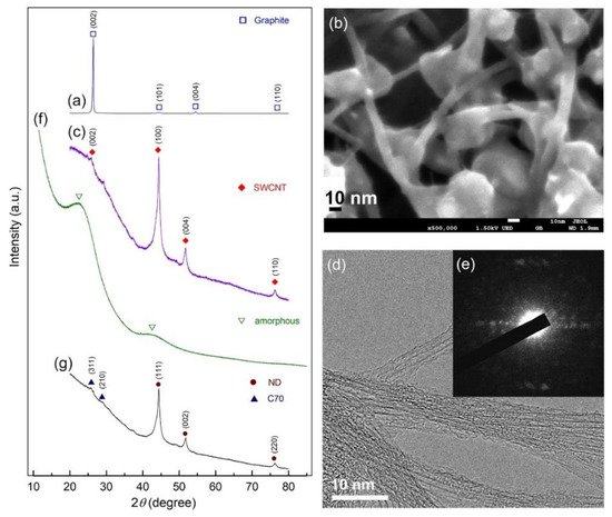
We used both X-ray diffraction (XRD) and field emission high resolution electron microscopy (FE-HRTEM) techniques to track the progress of phase transitions during high energy ball milling of graphite powders at various milling speeds. The XRD patterns of the beginning graphite powders acquired during the early stages of ball milling (0–16 h) are shown in
Figure 1. As illustrated in
Figure 1a, the initial graphite (G) powders had large-scaled crystallites, as evidenced by the sharp Bragg peaks corresponding to hexagonal close packed, hcp- (002), -(101), -(004), and -(110). After 10 h of ball milling, the pattern displayed Bragg peaks indicative of single wall carbon nanotubes, SWCNs (PDF# 00-58-1638), as illustrated in
Figure 1b
[27]. The high-magnification field emission scanning electron microscope (FE-SEM) micrograph of the powders obtained after this stage of milling (12 h) showed the existence of untransformed G-nanoparticles (10–30 nm in diameter) attached to the surface of the micron-size aggregates SWCNTs (
Figure 1b). Formation of metastable SWCNs was confirmed by XRD and HRTEM (
Figure 1c,d) as well as the corresponding nano beam diffraction pattern, NBDP (
Figure 1e)
[27].
Figure 1. XRD diffraction patterns and FE-SEM images of the powders obtained after ball milling for (a) 0 h, and (b) 12 h, respectively. In (c–e), the XRD patterns and corresponding FE-HRTEM, NBDP of the sample obtained after 10 h are shown. The XRD patterns for the samples milled for 16 h and 28 h are displayed in (f,g), respectively. micrograph of graphite powders produced after 0 and 12 h of high energy ball milling, respectively.
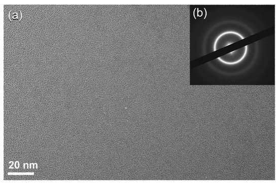
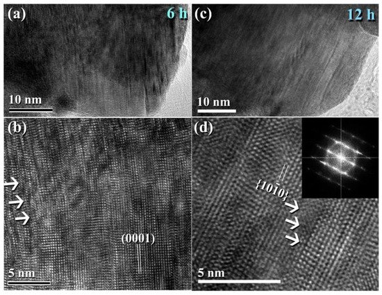
After 16 h of ball milling, the crystalline peaks associated with hcp-SWCNTs vanished completely and were replaced with homogenous halo-diffuse peaks, the first and second maxima of which were identified at 22.56° and 42.94°, respectively (
Figure 1f). This entails the transition of SWCNTs into amorphous carbon (a-C). HRTEM images corroborated the creation of the a-C phase, revealing a dense random-packing structure with a maze-like architecture, as illustrated in
Figure 2a. Untransformed G-nanoparticles, SWCNTs, and/or nano-carbon fibers are barely visible in this image, implying a full SWCNTs to a-C phase change. Moreover, the NBDP associated with a selected zone in
Figure 2b displays a halo-diffuse pattern of a typical amorphous phase (
Figure 2b)
[27].
Figure 2. (a) FE-HRTEM image and (b) corresponding NBDP of the sample obtained after 16 h of milling.
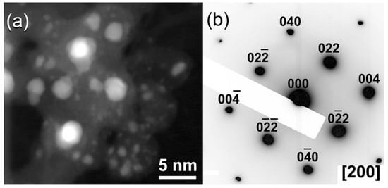
The dark field image (DFI) of the powders obtained after 28 h of ball milling is shown in
Figure 3a. Obviously, the particles possessed spherical-like crystallinity with rather wide particle size distribution, ranging between 1.8 nm to 4.8 nm in diameter (
Figure 3a). The NBDP of this fine particle is corresponding to NDs, as indexed by the zone axis (200) (
Figure 3b)
[27].
Figure 3. (a) Dark field image (DFI), and (b) corresponding NBDP of the sample obtained after 28 h of milling.
2.3. Tungsten Carbide
Among the hard materials, tungsten carbide (WC) has received considerable interest due to its unusual chemical and mechanical properties
[28]. WC is an interstitial combination of carbon atoms filling a W crystal
[28]. Since the early twentieth century, WC has been widely employed in the industry as cutting tool tips and wear-resistant parts. Due to its intrinsic resistance to oxidation and corrosion at elevated temperatures, WC is an excellent candidate for protective coatings for high-temperature electronics
[29][30]. Unfortunately, nanocrystalline bulk WC materials are rarely used in industrial scale applications due to their limited sinterability even at elevated temperatures (1650–1900 °C)
[31][32][33][34]. The possibility of improving mechanical properties including as hardness, elastic modulus, and fracture toughness has sparked interest in the manufacture of nanocrystalline WC ultrafine powders. Numerous methods, including chemical synthesis
[28], mechanically induced solid state reduction
[35], plasma-chemical interaction
[36], and chemical vapor deposition (CVD), can be employed to synthesize polycrystalline superfine WC powders with an average grain size of 300–40 nm. However, mechanical milling (MM) is believed to be the most potent approach for generating nanocrystalline WC ultrafine powders on an industrial scale at near room temperature
[33][35]. It has been demonstrated that ultrafine WC nanopowders with a spherical-like shape may be successfully generated employing WC milling equipment with a ball-to-powder weight ratio of 50:1
[33]. The milling procedure was carried out for 20 h at a speed of 400 rpm using a planetary-type ball mill.
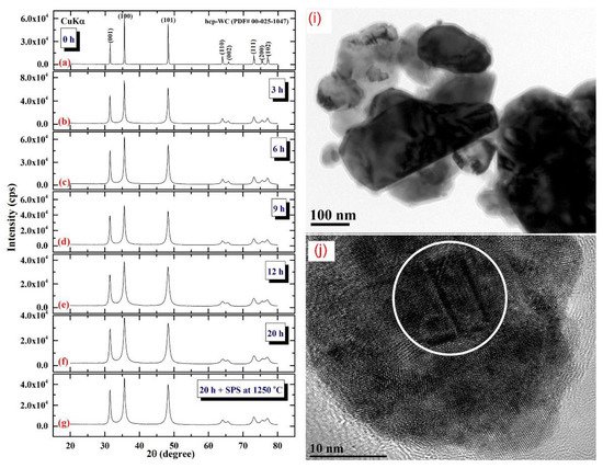
Figure 4 illustrates the XRD patterns of mechanically milled pure hcp-WC powders obtained after varying ball milling times ranging from 0 to 20 h. (Figure 4a–g). Figure 4a shows that as-received powders (0 h) had significant Bragg peaks that were consistent with polycrystalline hcp-WC (PDF# 00-025-1047). This starting material powder had a bulky look and was composed of large particles with an uneven shape, ranging in diameter from 50 to 600 nanometers (Figure 4i). The Bragg peaks of powders milled for 3–6 h MM time exhibited substantial broadening as a result of the grain refining process caused by the milling action (Figure 4b,c). The powders formed after three hours of MM exhibited nano-twin lattice defects and stuck faults in their interior structure, as illustrated in Figure 4j. Additionally, the diameters of the powder particles obtained after three hours of MM were substantially reduced to approximately 28 nm (Figure 4j). Following this stage of MM, the powders comprise a variety of grains ranging in size from 8 nm to 10 nm in diameter. During the intermediate stage (6–12 h), additional broadening of the Bragg peaks was seen, together with a significant drop in their intensities (Figure 4d,e), implying continuing grain refining and the formation of finer particles. Moreover, the WC powders suffered from a great number of lattice imperfections, where clear stacking faults and dislocations existed inside the dark-contrast grains (Figure 5a).
Figure 4. XRD patterns of ball milled WC powders treated for (a) 0, (b) 3, (c), 6 h, (d), 9 h, (e), 12, and (f), 20 h of milling. The powders produced after 20 h of milling and subsequently consolidated into bulk buttons at 1250 °C using the SPS method are depicted in the XRD (g). The bright field images (BFIs) of mechanically milled hcp-of-milling WC powders produced after 1 h and 3 h of high energy ball milling are shown in (i) and (j).
Figure 5. Lattice imperfections generated in WC crystals during the early stage of milling. HRTEM micrograph of ball milled WC powders after (a,b) 6 h, and (c,d) 12 h of milling.
The TEM micrograph of the bright-contrast region in
Figure 5a reveals the presence of severe dislocations, which are denoted by the symbols in
Figure 5b. These flaws were spread continually by increasing the MM time to 12 h (
Figure 5c), as indicated by the obvious staking errors in
Figure 5d. The plastic deformation of the WC crystal lattice that occurred during the early stages of MM was caused by slip and twinning, as illustrated in
Figure 5a. This mechanical deformation is favored to be concentrated into the shear bands comprising a high density network of dislocations
[37][38], as depicted in
Figure 5b. At this stage of MM, the strain at the atomic level grows as the dislocation density increases.
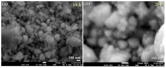
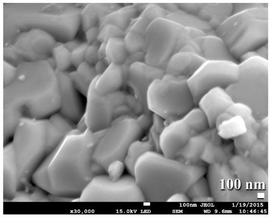
The FE-SEM micrograph demonstrates that the powders generated after 18 h of MM had a wide range of sizes (50–550 nm) and morphologies (bulky-, rugby ball-, and spherical-like shape), as illustrated in
Figure 6a. Following this step of MM, the WC powders shown in
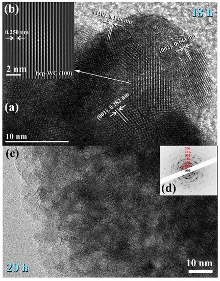
Figure 6a consisted of nano-sized grains (5–10 nm) of polycrystalline hcp-WC with various lattice planar orientations ((110), (002), (001), and (100)), as illustrated in
Figure 7a,b. Due to a decrease in the atomic level strain, the WC crystals were broken along their grain boundaries into nano-dimensional subgrains (
Figure 7a).
[33].
Figure 6. Micrographs FE-SEM ball milled WC powders after (a) 18, and (b) 20 h.
Figure 7. Images of FE-HRTEM for ball milled WC powders and their related selected area diffraction patterns (SADPs) are shown in (a,b) and (c,d), respectively.
At the conclusion of the MM processing time, the powders realized the benefits of the 20-h milling, showing broad Bragg peaks (
Figure 4f). This indicates that the MM process for generating WC nanopowders has been completed. Additionally, the intense ball-powders-ball (a) directed toward (0001) is illustrated in (b). In (d), the lattice resolution and NBDP of a specified area in (c) are combined
[33].
After 18–20 h of milling, the powders exhibited a nanospherical shape with an apparent diameter varying from 20 to 400 nm, as seen in Figure 13a,b. HRTEM micrograph of WC particles milled for 20 h (Figure 7c) As seen in Figure 7, the ultimate product generated after 20 h of MM had many gain boundaries with unpredictable crystallographic orientations (a, b). We should stress that extending the MM duration to 20 h was required to achieve homogenous WC cells with a narrow grain size dispersion (5–9 nm), as shown in Figure 7c.
Consolidation of WC with Spark Plasma Sintering
Consolidation of nanocrystalline WC powders is a key stage in establishing the powders’ physical/mechanical characteristics in a consistent and repeatable way, which is required for the majority of industrial and structural applications. Consolidating ultrafine powders into bulk, dense compacts while preserving nanoscale grain size is a serious challenge. Historically, hot pressing (HP) and hot isostatic pressing (HIP) methods were predominantly employed to consolidate WC powders between 1700 and 2000 °C
[29][30][33]. These typical consolidation regimes produced either green compacts (75% of theoretical density) with nanograin structure or dense compacts with microstructured grains. Due to the massive surface area of nanocrystalline material powders, they are extremely unstable and display significant grain development when subjected to high temperatures, such as those employed in HP and HIP. Historically, pure metallic powders like Co, Cr, and Ni have been added to the WC to speed up the sintering process and assure the formation of dense compacts. Unfortunately, the presence of a metallic matrix with such a low melting point has traditionally resulted in a variety of problems, including reduced hardness and corrosion/oxidation resistance, as well as increased grain development
[39].
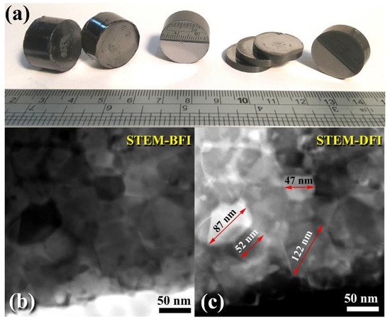
Spark plasma sintering (SPS) has attracted a significant number of researchers from the global societies of nanotechnology, materials science, and powder metallurgy due to its ability to preserve nanostructured nanopowders with low grain development. As a result, the SPS system has been primarily used to consolidate metastable materials (e.g., nanocrystalline powders) that are extremely temperature sensitive. SPS enables ultrafine powders to be sintered and bonded rapidly at lower temperatures than HP/HIP. Sintering is accomplished by electrically charging the spaces between powder particles and effectively applying a high-temperature spark plasma generated during a brief energizing stage, as well as an electro-magnetic field and/or joule heating via a continuous ON-OFF DC pulsed high electric current with a low voltage. The most effective components in the SPS consolidation process are the current effects and high heating rates. Figure 4g depicts the XRD pattern of as-consolidated WC-bulk button (Figure 8a). Clearly, no phase change occurred during the SPS-consolidation stage, as evidenced by the Bragg lines associated with hcp-WC (Figure 4g). By and large, the diffraction lines shown in Figure 4g exhibited significant widening, implying the presence of nanocrystalline WC grains. To assure the development of nanocrystalline bulk materials, an ion-slicer was used to produce a tiny portion of the as-consolidated WC button for TEM analysis. In Figure 8b,c, the STEM-bright field image (BFI) and the STEM-dark field image (DFI) for the as-consolidated bulk WC are displayed together. As-consolidated powders have a dense structure consisting of fine equiaxed grains, as seen in Figure 8b. However, because the SPS process was carried out in a short period of time and at a temperature (1250 °C), which is significantly lower than the temperature required for WC consolidation via hot pressing (above 1650 °C), and at a high heating rate (300 °C/min), the WC grains exhibited moderate grain growth (Figure 8a). The grain diameters of those dense WC buttons ranged from 47 to 122 nm, with an average diameter of 77 nm. By comparing this value to that of as-milled WC powders (7 nm), it is possible to deduce that the SPS method resulted in a modest grain growth of about tenfold when employed to consolidate WC nanocrystalline powders under the circumstances utilized for powder preparation and consolidation.
Figure 8. (a) A photograph demonstrating the shapes and sizes of various WC consolidated buttons obtained after the powders for the final product were consolidated (20 h) using the SPS method at 1250 °C. The STEM-BFI and STEM-DFI for the chosen button are depicted in (b) and (c), respectively.
This grain growth might be a result of the five-minute planned cooling procedure performed to bring the SPS system up to ambient temperature and remove the WC button from the graphite mold. Consolidation of the powders has been attempted at lower temperatures (800–1100 °C). Regrettably, those buttons that consolidated at such low temperatures had extremely low densities ranging from 12.38 to 14.26 g/cm3. By comparison, buttons consolidated at 1250 degrees Celsius had a high density of between 15.56 and 15.58 g/cm3. Additionally, FE-SEM micrographs of selected buttons solidified at 1250 °C indicate an exceptionally dense nanostructure morphology compatible with the formation of highly dense, fully formed WC prism-shaped fine grains, as seen in Figure 9.
Figure 9. FE-SEM image displays a fracture surface for consolidated WC bulk sample obtained upon SPS the as milled powders for 20 h at 1250 °C.
 +1 point