Blend materials refer to two or more polymers are formed by mixing together by physical or chemical methods, such as mixing block copolymers with block copolymers, block copolymers with homopolymers.
1. Introduction
In recent years, more and more attention has been paid to the self-assembly of block copolymers because it has great application prospects in the field of integrated circuits, biology, and many other fields. In the field of integrated circuits, nanostructures in electronic devices are fabricated by photolithography. Due to the diffraction limit of the radiation source, lithography faces inherent challenges in reducing the critical size to less than 20 nm. Thus, we need to discover a new technology to replace it. According to the international technology roadmap for semiconductors, the solutions of next-generation lithography mainly include extreme ultraviolet lithography [1][2][3], nanoimprint lithography [4][5][6], and block copolymer self-assembly [7][8]. At present, extreme ultraviolet lithography is the most widely used technology. However, its manufacturing cost is also the highest [9]. Nanoimprint requires a high-precision template, but the cost of template manufacturing is high, and the yield is limited. Block copolymer self-assembly has natural advantages over other technologies concerning cost and process. Block copolymer self-assembly can form hexagonal cylinders, cubic spheres, alternative lamellae, and bicontinuous gyroids. At the same time, the process of block copolymer self-assembly is relatively simple, which can greatly shorten the manufacturing time.
In the research into block copolymer self-assembly technology, it is necessary to constantly reduce the size of the structure and innovate the process. Nowadays, the self-assembly of block copolymers can form nanostructures of 1–100 nm
[10][11]. Researchers have explored the properties of block copolymers from the material itself, such as material synthesis, from the initial binary block copolymers to the present ternary or even multivariate block copolymers. In addition, a number of research groups have explored the self-assembly of block copolymers in many ways. On the one hand, the self-assembly morphology can be adjusted by changing the components of the two blocks in the binary block copolymer. On the other hand, the self-assembly morphology can be controlled by changing the molecular weight of the block copolymer. In order to obtain rich micro-region morphology of self-assembled block copolymers, researchers control and adjust the relevant process conditions to achieve this goal. For example, a temperature field
[12][13], temperature gradient field
[14][15], solvent field
[16][17][18][19][20], shear field
[21][22][23], magnetic field
[24][25][26][27][28], and electric field
[29][30][31] can be applied to control the morphology of self-assembled block copolymers. Both industry and academia have conducted a great deal of research into the morphology of field-regulated block copolymers. For example, Hashimoto et al. designed a temperature gradient instrument to control the microstructure of block copolymers
[15]. Kim and Libera have studied the effect of solvents on the morphology of triblock copolymer films under different evaporation rates
[17]. Morkved and his colleagues first studied block copolymer films on silicon nitride films under a plane electric field
[30].
2. Analysis on Results
2.1. Atmosphere Affects the Phase Separation
In order to accurately compare the phase separation changes of vacuum and air atmosphere, we chose the annealing temperature of 130 °C for the experiment because the morphology changes slowly with the temperature at this temperature, which is easier to compare.
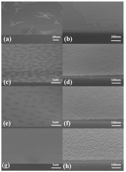
When the annealing atmosphere is air, the SEM results are as shown in Figure 1. When the annealing time was 10 min, the patterns formed in the shape of snowflakes in the SEM image (Figure 1a). No cylinders were formed in the film (Figure 1b). Increasing the annealing time to 20 min, the snowflake pattern changed to a block pattern (Figure 1c). At this time, patterned microdomains began to form (Figure 1d). When the annealing time was 30 min, the white block pattern disappeared into a black spot (Figure 1e), and the cylinders rose in number (Figure 1f). In addition, as the annealing time was 40 min, there was no special pattern on the surface of the thin film (Figure 1g). The formation of a regular cylindrical structure can be clearly observed (Figure 1h).
Figure 1. SEM images of air atmosphere annealing. The thickness of blend materials is about 20 nm. The annealing temperature is 130 °C, and the annealing time is different: (a,b) 10 min; (c,d) 20 min; (e,f) 30 min; (g,h) 40 min.
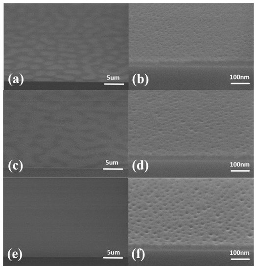
When the annealing atmosphere was a vacuum, the SEM results are as shown in Figure 2. When the annealing time was 10 min, the SEM showed a white block pattern (Figure 2a). At this time, the cylinders have formed (Figure 2b). After increasing the annealing time to 20 min, the white block pattern disappeared into black spots (Figure 2c). The number of cylinders increased (Figure 2d). As the annealing time was 30 min, there was no special pattern on the surface of the film (Figure 2e). The formation of a regular cylindrical structure can be clearly observed (Figure 2f).
Figure 2. SEM images of vacuum atmosphere annealing. The thickness of blend materials is about 20 nm. The annealing temperature is 130 °C, and the annealing time is different: (a,b) 10 min; (c,d) 20 min; (e,f) 30 min. The vacuum degree is −0.1 MPa.
Comparing the two experimental results, we found that there are different experimental phenomena between vacuum annealing and air annealing. Annealing in a vacuum atmosphere will cause the formation of white spots. While annealing in an air atmosphere, in addition to the formation of white spots, there will also be the formation of snowflake-like patterns. In addition, annealing in an air atmosphere takes longer to reach a stable structure of phase separation.
It is believed that the air atmosphere will lead to slower evaporation of the residual solvent. This is the main reason for the formation of snowflake-like structures and inhibition of the phase separation process.
2.2. Ratio Affects the Phase Separation
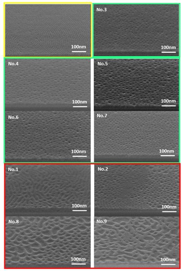
In order to explore the controllability of the blend ratio of PS-b-PC to PS, we designed nine groups of experiments (Table 1, in which the ratio of PS-b-PC to PS is the volume ratio). Experiment results are shown in Figure 3, in which the annealing temperature is 130 °C, the annealing time is 30 min, and the annealing atmosphere is a vacuum. Different sub-figures represent different blend ratios. Experimental results showed that cylindrical structures could be formed when the PS-b-PC to PS ratio is from 2.5:1 to 1:1.5 (experimental No. 3 to No. 7). Outside this range, cylinder cannot be formed, but there are other patterns.
Figure 3. SEM images of blend phase separation results. The annealing temperature is 130 °C, and the annealing time is 30 min. The thickness of blend materials is about 20 nm. The vacuum degree is −0.1 MPa.
Table 1. The experiment with different ratios.
| Experiment No. |
PS-b-PC |
Homopolymer(PS) |
| 1 |
3.5 |
1 |
| 2 |
3 |
1 |
| 3 |
2.5 |
1 |
| 4 |
2 |
1 |
| 5 |
1.5 |
1 |
| 6 |
1 |
1 |
| 7 |
1 |
1.5 |
| 8 |
1 |
2 |
| 9 |
1 |
2.5 |
In Figure 3, the yellow box is the layered structure formed by the phase separation of pure PS-b-PC; the pitch of lamellar is about 16 nm. The green box is the columnar structure formed by the phase separation of the blended material corresponding to experiments No. 3 to No. 7, in which the cylinder diameters are 12.36 nm, 13.09 nm, 15.12 nm, 14.26 nm, and 11.85 nm, respectively. The red boxes are other structures formed by the phase separation of the blended materials, in which experiments No. 1 and No. 2 formed a mixed structure of layered and porous, and experiments No. 8 and No. 9 formed irregular structures.
When the proportion of PS is low, layered and porous structures are formed. With an increase in the PS ratio, the microdomain area of the layered structure decreases, and the microdomain area of the porous structure increases. When PS-b-PC:PS reaches 2.5:1, self-assembly forms a columnar structure. When PS-b-PC:PS is 1:2, the structure becomes irregular.
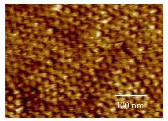
Figure 4 showed that the formation of the pattern is, in fact, cylinders.
Figure 4. AFM image of cylinders (corresponding to Figure 3 No. 7).
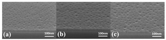
2.3. Molecular Weight Affects the Phase Separation
The influence of the molecular weight of the block copolymer on the quality of phase separation pattern was explored. Two new samples, samples 2 and 3, were added to the experiment, as shown in Table 2. Experiments showed that with an increase in molecular weight, the size of the cylinder increased (Figure 5). By comparing Figure 5a with Figure 5c, the results showed that the spacing between cylinders increased.
Figure 5. SEM images of blends materials phase separation results. The annealing temperature is 130 ℃, and the annealing time is 30 min: (a) sample no. 1; (b) sample no. 2; (c) sample no. 3. The vacuum degree is −0.1 MPa.
Table 2. The parameters of materials.
| Sample (PS-b-PC) No. |
Mn (g/mol) |
MW (g/mol) |
PDI |
| 1 |
7000 |
8100 |
1.157 |
| 2 |
11,700 |
13,600 |
1.162 |
| 3 |
15,100 |
17,000 |
1.125 |
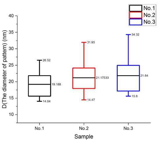
In order to reflect the experimental results more accurately, we collected and calculated the data extracted from the SEM images and plotted the result, as shown in Figure 5. The diameter of the structures was used to describe the dynamic process. Figure 6 shows the pattern diameters of the samples with different molecular weights. The average diameters of sample 1, sample 2, and sample 3 were 19.188 nm, 21.17533 nm, and 21.84 nm, respectively. With an increase in molecular weight, the size of the pattern increased but the pattern structure became sparse.
Figure 6. Box diagram of cylinder diameter for different samples.
 +1 point