Submitted Successfully!
To reward your contribution, here is a gift for you: A free trial for our video production service.
Thank you for your contribution! You can also upload a video entry or images related to this topic.
Version Summary Created by Modification Content Size Created at Operation
1 + 1804 word(s) 1804 2021-08-26 06:09:22 |
2 format correct + 53 word(s) 1857 2021-08-27 10:49:15 |

Video Upload Options

Do you have a full video?

Confirm

Are you sure to Delete?
Cite
If you have any further questions, please contact Encyclopedia Editorial Office.
Rossella, F. III-V Semiconductor Nanowire Ordered Arrays. Encyclopedia. Available online: https://encyclopedia.pub/entry/13603 (accessed on 20 April 2024).
Rossella F. III-V Semiconductor Nanowire Ordered Arrays. Encyclopedia. Available at: https://encyclopedia.pub/entry/13603. Accessed April 20, 2024.
Rossella, Francesco. "III-V Semiconductor Nanowire Ordered Arrays" Encyclopedia, https://encyclopedia.pub/entry/13603 (accessed April 20, 2024).
Rossella, F. (2021, August 26). III-V Semiconductor Nanowire Ordered Arrays. In Encyclopedia. https://encyclopedia.pub/entry/13603
Rossella, Francesco. "III-V Semiconductor Nanowire Ordered Arrays." Encyclopedia. Web. 26 August, 2021.
III-V Semiconductor Nanowire Ordered Arrays
Edit

Ordered arrays of vertically aligned semiconductor nanowires are regarded as promising candidates for the realization of all-dielectric metamaterials, artificial electromagnetic materials, whose properties can be engineered to enable new functions and enhanced device performances with respect to naturally existing materials. In this review we account for the recent progresses in substrate nanopatterning methods, strategies and approaches that overall constitute the preliminary step towards the bottom-up growth of arrays of vertically aligned semiconductor nanowires with a controlled location, size and morphology of each nanowire. While we focus specifically on III-V semiconductor nanowires, several concepts, mechanisms and conclusions reported in the manuscript can be invoked and are valid also for different nanowire materials.

semiconductor nanowire ordered arrays substrate patterning nanowire metasurfaces

1. Introduction

Semiconductor nanowires have emerged as a powerful class of materials with great potential for applications in many fields of technology, due to their outstanding electronic and optical properties and a relatively easy, controllable and scalable bottom-up growth process [1][2]. Their employment at large scale sets challenging requirements in terms of position, size and shape control of the individual nano-objects in nanowire ensembles [3][4]. This level of control represents a necessary step towards the realization of reliable and reproducible devices exploiting a very large number of nanowires for their operation, and for the integration of nanowire-based systems and devices with other technological platforms, such as silicon electronics and photonics [5][6]. Ordered arrays of vertically aligned semiconductor nanowires (NWs) have gained significant attention over the last two decades, as they have emerged as promising platforms in several fields of research including optics [7][8][9], electronics [10][11][12], energy [13][14][15][16], quantum computing [17][18], integrated photonics [19][20], sensing [21][22][23], and life sciences [24][25].

By exploiting the advances in nanofabrication and growth techniques, nanowire assemblies can nowadays be finely designed in order to fully tune and adjust their physical properties [26]. In particular, nanowire arrays can be engineered to realize nanowire metamaterials and metasurfaces, artificially prepared electromagnetic materials made of resonant subwavelength structures, showing effective medium properties that do not exist in nature. Photonic metamaterials made of assemblies of metal or semiconductor NWs have been experimentally and theoretically investigated [27][28]: nanowire metamaterials with optical negative refraction [29], optical cloaks [30], electrically tunable metamaterials [31], and near zero reflectance materials [32] have been reported.

As shown in the following sections, nanowires are available in a large variety of materials and they can incorporate heterostructures made of different components, even combining materials that are challenging to be combined in their thin film counterparts.

In this review we shine light on the recent progresses in the bottom-up realization of ordered arrays of vertically arranged semiconductor nanowires and nanowire metasurfaces by systematically reviewing the role of substrate pre-patterning, the current opportunities and the experimental limitations. Indeed, the realization of highly ordered nanowire arrays requires a preliminary step of substrate lithographic patterning, aimed at defining the specific nanowire locations on the substrate. Notably, the geometry and quality of the pattern employed to assist the nanowire growth dramatically affects the characteristics of the grown nanowire array. This study pinpoints and fixes the key concepts and phenomena guiding the subtle interdependence between surface pre-patterning and nanowire array growth. Such concepts and phenomena are typically common to several nanowire materials and growth approaches. In our study we devote particular attention to nanowire systems made of III-V semiconductor compounds; however, several mechanisms discussed for III-V’s can be invoked with minor differences for other semiconductors and semiconductor compounds.

2. Semiconductor Nanowires and Nanowire Arrays

A fundamental boost in nanowire research originated from the pioneering works of Lieber, Yang and Samuelson in the ‘90s, who were the first to demonstrate the possibility to realize, by using bottom-up self-assembling growth techniques, very high quality nanowires structures [33][34][35][36], thus sparking the interest of the scientific community in this field. In particular, they demonstrated the versatility of the bottom-up growth in enabling the realization, during growth, of very high quality nanowire crystals and heterostructures, made of combinations of different materials, resulting in very abrupt and atomically sharp interfaces. This opportunity is permitted by the strain relaxation along the nanowire sidewalls occurring in bottom-up growth, enabling the coupling of materials with a high lattice constant mismatch, such as, for example, III-V materials on silicon substrates [1][37][38]. Moreover, self assembling generally enables the realization of less defected surfaces and a better control of the resulting facets [1] with respect to top-down lithography approaches. These advantages made bottom-up self-assembling the most eligible approach for nanowire growth.

In recent years, new avenues for exploration in the nanowire field have been enabled by the advances in growth and nanofabrication techniques, which has allowed the design of engineered nanowire patterns with a fine control over the size, shape, material composition, location, and orientation of each individual nanowire.

Apart from the interest related to the exploration of new physical phenomena, such as advanced mechanisms of light propagation control at the nanoscale, the deterministic growth at selected locations on the substrate of nanowires represents the fundamental challenge to be addressed from the perspective of the full exploitation of nanowire potentialities in large scale applications, possibly with their integration with more mature (e.g., silicon-based) technological platforms [3][4].

With rare exceptions [39], most of the processes for the fabrication of ordered arrays of vertical nanowires, especially when high quality and high pattern precision is required, include at least one stage of lithographic patterning as the fundamental step to define the pattern geometry. As a matter of fact, the final outcome—the nanowire array—is dramatically affected not only by the specific growth parameters ruling the kinetics and thermodynamics of the growth mechanisms, but also by the geometry and quality of the pattern employed to assist the nanowire growth [3][40][41]. This is the reason why, in the context of ordered nanowire array realization, the role of the substrate patterning deserves a dedicated and accurate investigation: reviewing the investigation efforts spent by the scientific community in this direction is actually the goal of the present work.

3. Bottom-Up Approaches to the Realization of Ordered Arrays of Vertically Aligned Semiconductor Nanowires

The bottom-up approaches for the realization of ordered arrays of semiconductor nanowires mainly rely on two prominent techniques: nanoparticle-assisted growth, which is at present the most commonly used technique for NW growth [5][37][42], and catalyst–free growth, often obtained by selective area epitaxy. Both these techniques enable nanowires growth at specific locations predefined by lithographic prepatterning of the substrate.

The choice of the lithographic patterning technique for substrate preparation depends on the desired specifications of the array. The nanowires composing an engineered array can be individually seeded, or grown randomly on selected areas. In the latter case, for growth areas with a feature size above several hundreds of nanometers, or even micrometers, the catalyst pattern can simply be defined by resorting to micropatterning techniques (e.g., UV lithography or laser writing) and then the nanowire growth can be obtained by applying the same processes commonly employed for NW VLS growth on unpatterned substrates, e.g., thin metal layer deposition followed by thermal de-wetting or a standard deposition of metal colloidal nanoparticles [43]. However, studies on the role of the catalyst’s shape in an individually seeded nanowire suggest that for growth areas below a few hundreds of nanometers, a dedicated optimization of the growth parameters is definitively required [44] (See Section 3.1 ).

The most common technique exploited for the definition of precisely located metal seeds for ordered nanowire array realization is electron beam lithography (EBL) [45][46][47][44][48].

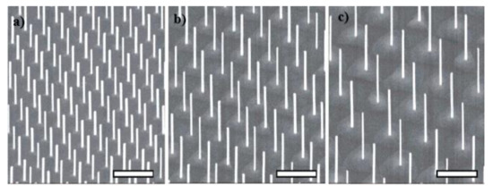
In Figure 1 some examples of InAs nanowire-ordered arrays grown on a prepatterned substrate realized by electron beam lithography are shown [49].

Figure 1. SEM tilted views of nanowire InAs NW arrays grown from EBLprepatterned substrates. The NWs have same diameters but different inter-wire distances: (a) 0.5 µm, (b) 0.75 µm and (c) 1 µm. The nanowires were grown from Au catalysts realized by electron beam lithography. Scale bar is 1 µm in each panel. (Reprinted with permission of Ref. [49]).

4. Influence of the Pattern Characteristics

The study of the role of the pattern characteristics, namely the metal seed size and the aspect ratio in metal-catalyzed growth, the hole sizes and aspect ratio in template assisted growth and the pitch, in enabling the reliable fabrication of uniform and controlled nanowire arrays, is sparsely addressed in the literature, but its crucial impact is fully recognized [3][40][44]. Some relevant information about the main mechanisms relating the pattern characteristics to the final array properties, as well as the connected experimental limitations in fabrication, can anyhow be gathered from the abundant literature in the growth field, which also includes some interesting recent papers and reviews [1][5]. Trying to put forward a comprehensive discussion including all the reported results, obtained for a large variety of nanowire materials, growth techniques and conditions, would be a very hard task, because the reported findings are most of the time dependent on the specific used growth conditions, adding a further complexity to the analysis.

For the growth conditions at which only axial growth occurs, the nanowire diameter is defined by the geometric parameters of the individual element in the pre-patterned substrate. As previously mentioned the current substrate patterning techniques allow to define the catalyst seeds and etching mask openings in the scale of a few nm diameter. However, the patterning technology resolution can be assumed only as a rough estimation of the lower NW diameter and array pitch, as the individual pattern featured size often does not correspond precisely to the nanowire size [5]. In VLS nanowire growth of III-V semiconductor compounds and other semiconductor materials, the nanowire diameter depends in first approximation on the seed particle volume, which includes both the starting catalyst droplet volume and the amount of the source materials incorporated into the seed [8][45]. Detailed models to explain the mechanism have been proposed [50][51]. During the initial stages of the growth, the catalyst nanoparticles will melt and often expand as they become saturated with the source materials, causing the nanowire diameter to exceed the initial catalyst particle size of several nanometers [44][52]. The contact angle formed by the metal catalyst and the nanowire growth facet, which is correlated to the catalyst stability at the nanowire tip, also plays a crucial role [5], affecting the diameter [5][53] and in some cases also the crystal structure [54], and growth direction [55]. Similarly, in selective area growth, the nanowire diameters are defined by the dimension of the openings in the growth mask. Moreover, in this case, the smallest diameter obtained for self-catalyzed growth is around 10 nm, which was obtained with an accurate control of the contact angle. In general, reaching nanowire diameters in the sub-30 nm range by bottom-up growth—which would enable quantum confinement functionalities—is presently considered a challenging task, and the possibility to realize large area arrays of controlled nanowires in that scale range still needs optimization [5][56][57]. Moreover, changes in diameter along the NW body (tapering and radial vapor-solid growth) and local random or non-random fluctuations of the diameter are often observed.

An alternative method to obtain a very high yield in catalyst-assisted growth is to adopt a combined approach, which exploits selective area growth, combined with a catalyst-assisted method [58].

Notably, the optimal control of the individual element geometry of the pattern is not sufficient to guarantee a very high yield in the final NW array: several other growth parameters need to be optimized, as will be briefly discussed in the sections that follow.

References

  1. Güniat, L.; Caroff, P.; Fontcuberta I Morral, A. Vapor phase growth of semiconductor nanowires: Key developments and open questions. Chem. Rev. 2019, 119, 8958–8971.
  2. LaPierre, R.R.; Robson, M.; Azizur-Rahman, K.M.; Kuyanov, P. A review of III–V nanowire infrared photodetectors and sensors. J. Phys. D Appl. Phys. 2017, 50, 123001.
  3. Vukajlovic-Plestina, J.; Kim, W.; Ghisalberti, L.; Varnavides, G.; Tütüncuoglu, G.; Potts, H.; Friedl, M.; Güniat, L.; Carter, W.C.; Dubrovskii, V.G.; et al. Fundamental aspects to localize self-catalyzed III-V nanowires on silicon. Nat. Commun. 2019, 10, 869.
  4. Tomioka, K.; Yoshimura, M.; Fukui, T.A. III–V nanowire channel on silicon for high-performance vertical transistors. Nature 2012, 488, 189–192.
  5. McIntyre, P.C.; Fontcuberta I Morral, A. Semiconductor nanowires: To grow or not to grow? Mater. Today Nano 2020, 9, 100058.
  6. Barrigonemar, B.; Samuelson, L. Synthesis and applications of III–V nanowires. Chem. Rev. 2019, 119, 9170–9220.
  7. Lin, S.Y.; Chow, E.; Hietala, V.; Villeneuve, P.R.; Joannopoulos, J.D. Experimental demonstration of guiding and bending of electromagnetic waves in a photonic crystal. Science 1998, 282, 274–276.
  8. Fan, Z.; Kapadia, R.; Leu, P.W.; Zhang, X.; Chueh, Y.-L.; Takei, K.; Yu, K.; Jamshidi, A.; Rathore, A.A.; Ruebusch, D.J. Ordered arrays of dual-diameter nanopillars for maximized optical absorption. Nano Lett. 2010, 10, 3823–3827.
  9. Demontis, V.; Marini, A.; Floris, F.; Sorba, L.; Rossella, F. Engineering the optical reflectance of randomly arranged self-assembled semiconductor nanowires. AIP Conf. Proc. 2020, 2257, 020009.
  10. Larrieu, G.; Han, X.L. Vertical nanowire array-based field effect transistors for ultimate scaling. Nanoscale 2013, 5, 2437.
  11. Thelander, C.; Agarwal, P.; Brongersma, S.; Eymery, J.; Feiner, L.F.; Forchel, A.; Scheffler, M.; Riess, W.; Ohlsson, B.J.; Goesele, U.; et al. Nanowire-based one-dimensional electronics. Mater. Today 2006, 9, 28–35.
  12. Chandra, N.; Tracy, C.J.; Cho, J.H.; Picraux, S.T.; Hathwar, R.; Goodnick, S.M. Vertically grown Ge nanowire Schottky diodes on Si and Ge substrates. J. Appl. Phys. 2015, 118, 024301.
  13. Garnett, E.; Yang, P. Light trapping in silicon nanowire solar cells. Nano Lett. 2010, 10, 1082–1087.
  14. Goktas, N.I.; Wilson, P.; Ghukasyan, D.; Wagner, D.; McNamee, S.; LaPierre, R.R. Nanowires for energy: A review. Appl. Phys. Rev. 2018, 5, 041305.
  15. Kelzenberg, M.; Boettcher, S.; Petykiewicz, J.; Turner-Evans, D.B.; Putnam, M.C.; Warren, E.L.; Spurgeon, J.M.; Briggs, R.M.; Lewis, N.S.; Atwater, H.A. Enhanced absorption and carrier collection in Si wire arrays for photovoltaic applications. Nat. Mater. 2010, 9, 239–244.
  16. Wallentin, J.; Anttu, N.; Asoli, D.; Huffman, M.; Aberg, I.; Magnusson, M.H.; Siefer, G.; Fuss-Kailuweit, P.; Dimroth, F.; Witzigmann, B.; et al. InP nanowire array solar cells achieving 13.8% efficiency by exceeding the ray optics limit. Science 2013, 339, 1050–1060.
  17. Schüffelgen, P.; Schmitt, T.; Schleenvoigt, M.; Rosenbach, D.; Perla, P.; Jalil, A.R.; Mussler, G.; Lepsa, M.; Schäpers, T.; Grützmacher, D. Exploiting topological matter for Majorana physics and devices. Solid-State Electron. 2019, 155, 99–104.
  18. Gibson, S.J.; van Kasteren, B.; Tekcan, B.; Cui, Y.; van Dam, D.; Haverkort, J.E.M.; Bakkers, E.P.A.M.; Reimer, M.E. Tapered InP nanowire arrays for efficient broadband high-speed single-photon detection. Nat. Nanotechnol. 2019, 14, 473–479.
  19. Kim, H.; Lee, W.; Farrell, A.C.; Morales, J.S.D.; Senanayake, P.; Prikhodko, S.V.; Ochalski, T.J.; Huffaker, D.L. Monolithic InGaAs nanowire array lasers on silicon-on-insulator operating at room temperature. Nano Lett. 2017, 17, 3465–3470.
  20. Yan, R.; Gargas, D.; Yang, P. Nanowire photonics. Nat. Photonics 2009, 3, 569–576.
  21. Liao, Y.L.; Zhao, Y. Ultra-narrowband dielectric metamaterial absorber with ultra-sparse nanowire grids for sensing applications. Sci. Rep. 2020, 10, 1480.
  22. Patolsky, F.; Lieber, C.M. Nanowire nanosensors. Mater. Today 2005, 8, 20–28.
  23. Offermans, P.; Crego-Calama, M.; Brongersma, S.K. Gas detection with vertical InAs nanowire arrays. Nano Lett. 2010, 10, 2412–2415.
  24. Elnathan, R.; Kwiat, M.; Patolsky, F.; Voelcker, N.H. Engineering vertically aligned semiconductor nanowire arrays for applications in the life sciences. Nano Today 2014, 9, 172–196.
  25. Muskens, O.L.; Diedenhofen, S.L.; van Weert, M.H.M.; Borgström, M.T.; Bakkers, E.P.A.M.; Gómez Rivas, J. Epitaxial growth of aligned semiconductor nanowire metamaterials for photonic applications. Adv. Fun. Mat. 2008, 18, 103–1046.
  26. Quan, L.N.; Kang, J.; Ning, C.Z.; Yang, P. Nanowires for Photonics. Chem. Rev. 2019, 119, 9153–9169.
  27. Simovski, C.; Belov, P.; Atrashchenko, A.V.; Kivshar, Y. Wire metamaterials: Physics and applications. Adv. Mater. 2010, 24, 4229–4248.
  28. Tsai, K.; Wurtz, G.A.; Chu, J.; Cheng, T.; Wang, H.; Krasavin, A.V.; He, J.; Wells, B.M.; Podolskiy, V.A.; Wang, J. Looking into meta-atoms of plasmonic nanowire metamaterial. Nano Lett. 2014, 14, 4971–4976.
  29. Yao, J.; Liu, Z.; Liu, Y.; Wang, Y.; Sun, C.; Bartal, G.; Stacy, A.M.; Zhang, X. Optical negative refraction in bulk metamaterials of nanowires. Science 2008, 321, 930.
  30. Cai, W.; Chettiar, U.K.; Kildishev, A.V.; Shalaev, V.M. Optical cloaking with metamaterials. Nat. Photonics 2007, 1, 224–227.
  31. Salary, M.M.; Mosallaei, H. Electrically tunable metamaterials based on multimaterial nanowires incorporating transparent conductive oxides. Sci. Rep. 2017, 7, 10055.
  32. Yang, Z.P.; Ci, L.; Bur, J.A.; Lin, S.Y.; Ajayan, P.M. Experimental observation of an extremely dark material made by a low-density nanotube array. Nano Lett. 2008, 8, 446–451.
  33. Duan, X.; Lieber, C.M. Laser-assisted catalytic growth of single crystal gan nanowires. J. Am. Chem. Soc. 2000, 122, 188–189.
  34. Hu, J.T.; Min, O.Y.; Yang, P.D.; Lieber, C.M. Controlled growth and electrical properties of heterojunctions of carbon nanotubes and silicon nanowires. Nature 1999, 399, 48–51.
  35. Wu, Y.; Yang, P. Germanium nanowire growth via simple vapor transport. Chem. Mater. 2000, 12, 605–607.
  36. Samuelson, L.; Carlsson, S.B.; Junno, T.; Xu, H.; Montelius, L. Real time control of nanowire formation. Nanoscale Sci. Technol. 1998, 348, 19–22.
  37. Gazibegovic, S.; Car, D.; Zhang, H.; Balk, S.C.; Logan, J.A.; de Moor, M.W.A.; Cassidy, M.C.; Schmits, R.; Di, X.; Wang, G. Epitaxy of advanced nanowire quantum devices. Nature 2017, 548, 434–438.
  38. Caroff, P.; Messing, M.E.; Borg, B.M.; Dick, K.A.; Deppert, K.; Wernersson, L.E. InSb heterostructure nanowires: MOVPE growth under extreme lattice mismatch. Nanotechnology 2009, 20, 495606.
  39. Detz, H. Lithography-free positioned GaAs nanowire growth with focused ion beam implantation of GaH. J. Vac. Sci. Technol. B 2017, 35, 011803.
  40. Gibson, S.J.; LaPierre, R.R. Model of patterned self-assisted nanowire growth. Nanotechnology 2014, 25, 415304.
  41. Heiss, M.; Russo-Averchi, E.; Dalmau-Mallorquí, A.; Tütüncüoğlu, G.; Matteini, F.; Rüffer, D.; Conesa-Boj, S.; Demichel, O.; Alarcon-Lladó, E.; Fontcuberta I Morral, A. III–V nanowire arrays: Growth and light interaction. Nanotechnology 2014, 25, 014015.
  42. Dasgupta, N.P.; Sun, J.; Liu, C.; Brittman, S.; Andrews, S.C.; Lim, J.; Gao, H.; Yan, R.; Yang, P. Semiconductor Nanowires– + Synthesis, Characterization, and Applications. Adv. Mater. 2014, 6, 2137–2184.
  43. Hochbaum, A.I.; Fan, R.; He, R.; Yang, P. Controlled growth of Si nanowire arrays for device integration. Nano Lett. 2005, 5, 457–460.
  44. Mårtensson, T.; Borgstrom, M.; Seifert, W.; Ohlsson, B.J.; Samuelson, L. Fabrication of individually seeded nanowire arrays by vapour–liquid–solid growth. Nanotechnology 2003, 14, 1255–1258.
  45. Mårtensson, T.; Carlberg, P.; Borgström, M.; Montelius, L.; Seifert, W.; Samuelson, L. Nanowire arrays defined by nanoimprint lithography. Nano Lett. 2004, 4, 699.
  46. Dalacu, D.; Kam, A.; Austing, D.G.; Wu, X.; Lapointe, J.; Aers, G.C.; Poole, P.J. Selective-area vapour–liquid–solid growth of InP nanowires. Nanotechnology 2009, 20, 395602.
  47. Kawaguchi, K.; Sudo, H.; Matsuda, M.; Ekawa, M.; Yamamoto, T.; Arakawa, Y. Position-controlled InP nanowires with 10–100 μm pitches using Au-deposited SiO2/InP patterned substrates. Appl. Phys. Lett. 2014, 104, 063102.
  48. Pierret, A.; Hocevar, M.; Diedenhofen, S.L.; Algra, R.E.; Vlieg, E.; Timmering, E.C.; Verschuuren, M.A.; Immink, G.W.G.; Verheijen, M.A.; Bakkers, E.P.A.M. Generic nano-imprint process for fabrication of nanowire arrays. Nanotechnology 2010, 21, 065305.
  49. Jensen, L.E.; Björk, M.T.; Jeppesen, S.; Persson, A.I.; Ohlsson, B.J.; Samuelson, L. Role of surface diffusion in chemical beam epitaxy of InAs nanowires. Nano Lett. 2004, 4, 1961–1964.
  50. Lin, S.K.; Crawford, S.; Hoberfehlner, G.; Gradečak, S. Controlled Modulation of Diameter and Composition along Individual III–V Nitride Nanowires. Nano Lett. 2013, 13, 331–336.
  51. Schmidt, V.; Wittemann, J.V.; Senz, S.; Gösele, U. Silicon nanowires: A review on aspects of their growth and their electrical properties. Adv. Mater. 2009, 21, 2681–2702.
  52. Wu, Y.; Yang, P. Direct observation of vapor−liquid−solid nanowire growth. J. Am. Chem. Soc. 2001, 123, 3165–3166.
  53. Tersoff, J. Stable self-catalyzed growth of III–V nanowires. Nano Lett. 2015, 15, 6609–6613.
  54. Jacobsson, D.; Panciera, F.; Tersoff, J.; Reuter, M.C.; Lehman, S.; Hofmann, S.; Dick, K.A.; Ross, F.M. Interface dynamics and crystal phase switching in GaAs nanowires. Nature 2016, 531, 317–322.
  55. Wang, J.; Plissard, S.; Verheijen, M.A.; Feiner, L.F.; Cavalli, A.; Bakkers, E.P.A.M. Reversible switching of InP nanowire growth direction by catalyst engineering. Nano Lett. 2013, 13, 3802–3806.
  56. Del Giudice, F.; Becker, J.; de Rose, C.; Döblinger, M.; Suomenniemi, L.; Treu, J.; Riedl, H.; Finley, J.J.; Koblmüller, J. Ultrathin catalyst-free InAs nanowires on silicon with distinct 1D sub-band transport properties. Nanoscale 2020, 42, 21857–21868.
  57. Kim, W.; Dubrovskii, W.G.; Vukajlovic-Plestina, J.; Tütüncüoglu, G.; Francaviglia, L.; Güniat, L.; Potts, H.; Friedl, M.; Leran, J.B.; Fontcuberta I Morral, A. Bistability of contact angle and its role in achieving quantum-thin self-assisted GaAs nanowires. Nano Lett. 2018, 18, 49–57.
  58. Mohan, P.; Motohisa, J.; Fukui, T. Fabrication of InP/InAs/InP core-multishell heterostructure nanowires by selective area metalorganic vapor phase epitaxy. Appl. Phys. Lett. 2006, 88, 133105.
More
Information
Contributor MDPI registered users' name will be linked to their SciProfiles pages. To register with us, please refer to https://encyclopedia.pub/register :
View Times: 431
Revisions: 2 times (View History)
Update Date: 27 Aug 2021
1000/1000