This paper reviews the research and development of micromachined accelerometers with a noise floor lower than 1 µg/√Hz. Firstly, the basic working principle of micromachined accelerometers is introduced. Then, different methods of reducing the noise floor of micromachined accelerometers are analyzed. Different types of micromachined accelerometers with a noise floor below 1 µg/√Hz are discussed.
1. Introduction
High-resolution accelerometers are required for many specific application areas, including inertial navigation, earthquake detection, spacecraft guidance or stabilization, geophysical sensing, etc. The history of high-resolution accelerometers dates back to the 1960s, when they were used in space environment exploration missions. In the early 1970s, the Office National d’Etudes et de Recherches Aérospatiales (ONERA, France) developed an electrostatic accelerometer termed Capteur Accelerometrique Triaxial Ultra Sensible (CACTUS), designed for testing satellites, reaching a resolution of 10
−9 m/s
2 [1]. Shortly after, several similar high-resolution sensors were developed, such as the Super STAR and GRADIO accelerometers, which were employed for different satellites to conduct earth field recovery missions
[2]. These early high-resolution accelerometers were macroscopic devices of large size and heavy weight, as well as high cost, and were fabricated by conventional macro-machining methods.
Compared to conventional macroscopic high-resolution accelerometers, micromachined accelerometers feature many benefits, such as small size, light weight, low cost, low power and easy integration with semiconductor technology. According to Middelhoek
[3], the first Micro-Electro–Mechanical System (MEMS) accelerometer was developed by Vaganov in 1975, but he never published his work, as he was a visiting scientist from the USSR at Stanford University. Four years later, a piezoresistive MEMS accelerometer was developed by Roylance and Angell
[4] (1979), reaching a resolution of a few mg and a bandwidth higher than 1 kHz. In the 1990s, driven by the development of automotive airbags, MEMS accelerometers took a huge step in their development, as they met the requirements for airbag systems (i.e., low cost, miniature in size, good reliability and the ability to detect the sharp acceleration shock generated by a car crash). In 1990, a MEMS accelerometer was put into an automobile for the first time and, in 2007, over 100 million MEMS accelerometers were sold that year
[5]. More recently, smartphones have opened a considerable new market for MEMS accelerometers, as every smartphone produced nowadays contains a three-axis MEMS accelerometer
[6]. These MEMS accelerometers have relatively low performance characteristics compared to high performance sensors used for the aforementioned applications; this is illustrated in
Table 1 [5].
Table 1. Typical specifications of MEMS accelerometers on three performance levels, including tactical grade, navigation grade as well as auto control
[5].
| Parameters |
Navigation Grade |
Tactical Grade |
Consumer Grade |
| Input range |
±1 g |
±5 g |
±50 g |
| Noise |
<50 μg |
<100 μg |
<50 mg |
| Working Frequency |
100 Hz |
100 Hz |
400 Hz |
| Sensitivity |
<100 μg |
<200 μg |
<50 mg |
| Nonlinearity |
<0.05% |
<0.1% |
<2% |
| Max shock input |
>10 g |
>20 g |
>2000 g |
| Partial axis sensitivity |
<0.1% |
<0.3% |
<5% |
Various micromachined accelerometers have been reported in the last two decades. In 1998, a detailed review of micromachined inertial sensors was reported in which different categories of micromachined accelerometers and their key technologies were discussed
[7]. However, the mechanical designs and the associated interface circuits of micromachined accelerometers have been evolving rapidly in recent years. In 2015, a review of high-g micromachined accelerometers was presented in
[8]. However, low-g micromachined accelerometers (accelerometers with a sub-µg resolution are not discussed in
[8].
2. MEMS Accelerometers with Vacuum Packaging
Since TNEA is inversely proportional to Q, the inherent noise floor of the accelerometer can be reduced by improving Q through vacuum packaging if the proof mass weight suspension spring constant of a MEMS accelerometer remains unchanged. However, high Q results in sensors with long settling time and large overshoot, thus require a closed-loop system to maintain a stable measurement, which may, to some extent, compromise the benefit of low TNEA due to high Q.
Wu et al.
[9] (2006) at Carnegie Mellon University presented a detailed theoretical analysis and simulation of a high order multibit force feedback electro–mechanical ΣΔM for MEMS accelerometers with high Q. However, there was no further update of the related experimental results. Aaltonen et al.
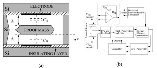
[10][11] (2009) at Helsinki University of Technology developed an accelerometer with a high Q (Q > 700) and a 1 kHz fundamental frequency, as shown in
Figure 1. The accelerometer was vacuum packaged and operated in a closed-loop control system, which maintained loop stability by damping the Q of the system through electrostatic force feedback. The accelerometer reached a resolution of 300 ng/√Hz (at 30 Hz) with a dynamic range of ±1.5 g and a signal bandwidth of 300 Hz. Xu et al.
[12] (2015) at Harbin Institute of Technology developed a closed-loop switched-capacitor ΣΔM CMOS interface circuit for a micromechanical capacitive accelerometer with a noise floor of lower than 200 ng/√Hz (at 100 Hz) and a dynamic range of ±1.2 g. The control loop was implemented in a distributed feedback and feedforward topology, dampening the high Q sensing element by the application of an electrostatic feedback force and phase compensation, which introduced an extra zero to stabilize the loop.
Figure 1. Schematic diagrams of the MEMS accelerometer and its closed-loop system developed by Aaltonen et al. at Helsinki University of Technology
[10][11]: (
a) schematic of the MEMS accelerometer; (
b) block diagram of the closed-loop control system.
The company Honeywell
[13] developed a micromachined accelerometer (QA-3000) using a suspension and proof mass made of quartz, which has a lower material damping compared with silicon and can be used to develop devices with high Q. The small proof mass and the high spring constant of the suspension were compensated significantly by high Q, yielding a noise floor lower than 1 µg/√Hz, a bandwidth larger than 300 Hz as well as a full-scale range of ±60 g.
High Q reduces the TNEA of a MEMS accelerometer. However, for a MEMS accelerometer with high Q, the requirements of a closed-loop system control and vacuum packaging increase their complexity and cost, as well as power consumption. Additionally, electronic components from the closed-loop system introduce more electronic noise and thus increase the overall noise floor of the sensor, which may, to some extent, compromise the benefit of low TNEA due to high Q. Thus, such a type of accelerometer is only used for specialized applications.
3. MEMS Accelerometers with a Low Noise Interface Circuit
Typically, a MEMS accelerometer generates a proof mass displacement in response to an acceleration input, which needs to be transferred into an electronic signal through an interface circuit. However, the noise introduced by those circuits limits the resolution of the MEMS accelerometer. Thus, designers tried to optimize the interface circuit to improve the resolution of MEMS accelerometers.
Si-Ware System (now part of Goodix Technology)
[14] developed different ASICs, such as SWS1110, SWS61111 and SWS1120, as well as SWS1130, for capacitive MEMS inertial sensors with an input circuit noise of less than 50 zF/√Hz. The SWS1110 is a configurable ASIC, in which its front-end parameters can be adjusted to work with various inertial sensors in open-loop or closed-loop modes.
Utz et al.
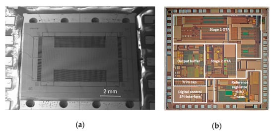
[15] (2018) at the Fraunhofer Institute for Microelectronic Circuits and Systems also developed a capacitance to voltage ASIC with an input noise of 50 zF/√Hz within a bandwidth of 10 Hz to 10 kHz, as shown in
Figure 2. The core of the readout circuit was a two-stage, fully differential, chopper-stabilized amplifier in which a chopping frequency of 833 kHz was selected to reduce the low frequency noise, mainly due to flicker noise. With this interface circuit, a conventional MEMS accelerometer with large proof mass achieved a noise floor of 216 ng/√Hz (at 30–40 Hz) and a large bandwidth of 5 kHz. This MEMS accelerometer operated in open-loop mode at atmospheric pressure, hence it did not require a closed-loop control system, reducing the complexity of the system and cost for vacuum packaging.
Figure 2. Images of the MEMS accelerometer and the readout ASIC developed by Utz et al. at Fraunhofer Institute for Microelectronic Circuits and Systems
[15]: (
a) SEM image of the MEMS accelerometer; (
b) photograph of the readout ASIC.
Kamada and Furubayashi et al.
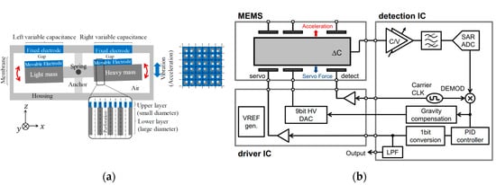
[16][17] (2019) at Hitachi developed a capacitive MEMS accelerometer with an asymmetric so-called “teeter-totter structure” in a getter-free vacuum ceramic package, which reached a noise floor lower than 30 ng/√Hz (at 10–300 Hz) and a dynamic range of 116 dB with a power consumption of 20 mW. It was intended for large sensor network applications, as shown in
Figure 3.
Figure 3a shows the teeter-totter structure, consisting of a proof mass comprising a heavy mass on one side and a light mass on the other side. The proof mass was suspended with four torsional springs. Pick-off capacitors were formed between the fixed and the moveable electrodes on the proof mass surface. In this configuration, the weight imbalance between the heavy mass and the light mass made the two masses vibrate in opposite directions, resulting in an output capacitance change under a
z-axis acceleration. To achieve high resolution, different noise sources were addressed by different means. To generate high Q and reduce the Brownian noise, specially designed two-sized perforations were fabricated in the device and substrate layers of the proof mass, in which the upper plate had smaller diameter holes and the lower plate had large ones, as shown in
Figure 3a
[18]. The Q of the device was 3400 in a getter-less vacuum ceramic package with a pressure of about 6–10 Pa. The 1/f noise of the analog chain was shifted out of the band by modulating ΔC with a 500 kHz pulse applied to the detection capacitors through the driver capacitors. Then, the modulated ΔC signal was demodulated before the proportional–integral–derivative (PID) controller. High-voltage (HV) MOS transistors with channel lengths of 8 μm and widths of several tens of millimeters were adopted for the input differential pair of the voltage-follower to reduce 1/f noise. A PID controller suppressed the in-band 1-bit quantization noise. A digital bandpass ΣΔM modulator created a notch in the quantization noise between 20 and 30 kHz. By isolating the servo- and gravity-compensation capacitors from the op-amp input with the insulation layers, the thermal noise of the front C/V amplifier was suppressed. The servo-signal leakage was still present due to the residual mismatch of the two parasitic capacitances, although it was inherently blocked by an isolation structure. The leakage signal was subtracted from the ADC output by the 1-bit servo-signal after being shaped by a finite impulse response (FIR) filter, whose magnitude of leakage and tap coefficients were chosen by a least mean square (LMS) algorithm. Besides, noise was generated by the coupling between the MEMS higher-order resonant modes and the high-frequency components of the 1-bit quantization noise. To reduce this noise, a digital bandpass delta–sigma modulator (DBPDSM) was used to generate the 1-bit servo-signal instead of the 1-bit quantizer alone, since the former could create a high-frequency notch while preserving the low-frequency signal components. By tuning a parameter of the DBPDSMT, the position of the notch was placed in the region where the higher-order resonances are densely located.
Figure 3. Schematic diagrams of the MEMS accelerometer and the closed-loop system and its closed-loop control system developed by Kamada and Furubayashi et al. at Hitachi
[16][17]: (
a) teeter-totter structure of the MEMS accelerometer with perforations; (
b) overall block diagram of the closed-loop control system of the MEMS accelerometer.
In general, an ASIC interface circuit has lower noise and lower power consumption, as well as smaller size and lower cost for high volume markets compared to a printed circuit board (PCB) interface circuit. Thus, the integration of an ASIC interface circuit with a MEMS accelerometer to achieve a low noise floor has become standard nowadays. However, it requires specialized expertise and often requires several years of development time. Therefore, a PCB interface circuit is preferable for prototype testing.
 +1 point